Design and Analysis of Novel Charge Pump
Architecture for Phase Locked Loop
Manoj Sharma, Gajendra Sujediya
Research Scholar, M.Tech . VLSI, RIET, Jaipur, Rajastan, India
Astt. Professor, RIET Jaipur, Rajasthan, india
ABSTRACT: Charge pump circuit is widely used in integrated circuits (ICs) due to the continuous power supply
reduction which is dedicated to several kind of applications of low voltage phase locked loop (PLL), flash Memories & DRAM’s smart power, switched capacitor circuits, non-volatile memories, operational amplifiers, voltage regulators, SRAMs, LCD drivers, piezoelectric actuators, Radio frequency antenna switch controllers, etc. Charge pump are used in these application, basically it is DC to DC converter which have capacitor instead of an inductor or transformer for energy storage. Thereby it is able to generate to higher voltage than power supply voltage. Designing of charge pump depend on the structure of MOS transistors as switches. CMOS charge pump is appropriate for low voltage applications, can be activating with very low supply voltage. Conversely, the voltage drop and body effect of MOS transistor decrease the performance of the charge pump when the number of stages is lift up so that only 4-stage of various charge pump topologies have been implemented in this thesis such as Dickson, static, dynamic, with control scheme, with cross connected NMOS cell.
Motivation
Electronic devices have become inseparable parts of people’s lives in modern times for portable consumer. The basic requirements of the people’s are portable, thin, lightweight and multifunctional consumer electronic devices such that mobile phone, laptops is increasing day-to-day. These portable devices are charged from single battery and they should be capable to operate for an extended phase of time. In electronics industry, there are lot of devices usually have a large number of circuit sub-systems which require different voltage domains to conduct the device. Consequently, the requirement for multiple voltage creation from a single voltage battery operated power supply imposes design challenges to achieve high voltage conversion efficiency, low power dissipation low output ripple voltage and low reverse current.
Objective
The objective of this thesis is to design and implementation of different types of charge pump based on performance factors namely speed, power and output voltage, output current, voltage conversion. This thesis provides the comparative study of design and implementation of Dickson charge pump, static charge pump, dynamic charge pump, charge pump with CTS control scheme, charge pump with cross connected NMOS cells. The core objectives are, to study about charge pump importance and existence of these devices in low power and high speed system, design and implementation of different types of charge pump and the comparative study of design and implementation of charge pump.
Basic of charge pump
The system which is battery-operated, low voltage CMOS design becomes necessary for low power dissipation. Thus, the supply voltages continue to scale down. Certain parts of the system may be requiring higher voltage for proper working. Therefore, charge pump circuit is likely to become a crucial component in low power CMOS design.
Charge pump
switching converter which is used to offers a output voltage beyond the normally available supply voltage Vdd rails, such as a voltage higher than the input or a reversed polarity voltage. Voltage can be step-up, step-down and inverted by using charge pump. The charge pump can provide current of less than 100 mA [33].
Fig. 1 Block diagram of a generic charge pump
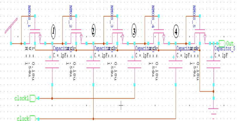
I. IMPLEMENTATION OF CHARGE PUMPDickson charge pump
The Dickson charge pump consist of diode connected five MOS transistor, five capacitor and two pumping clocks as shown in fig: 2. The charges in the Dickson charge pump can be flow only in one direction due to MOS transistor. This charge pump has 2-phase non overlapping clock pulse namely clock and clock1. The amplitude of the clocks is
equivalent to amplitude of power supply voltage VDD. The diode connected NMOS are used to transfer charges from
input to output in each stage.
The functional workings of Dickson charge pump as follows:
Case I: When the Clock is low and clock1 is high
Then NMOS_1, NMOS_3, and NMOS_5 are turned on and NMOS_2 & NMOS_4 are switched off, after that the charge is transferred to node1 from VDD, the charge in node 2 is transferred to node 3, and the charge in node 4 is transferred to Vout.
Case II: When the Clock is high and clock1 is low
Then NMOS_2 and NMOS_4 are turned on and MNOS_1 & MNOS_3 switched off, After that the charge is transferred to node 2 from node 1, and charge in node 3 is transferred to node 4[20]. Therefore, the output voltage of Dickson charge pump circuit is:
= ( − )
Where
Vtn = threshold voltage of the diode-connected NMOS in the i-th stage and
N = stage number of stage
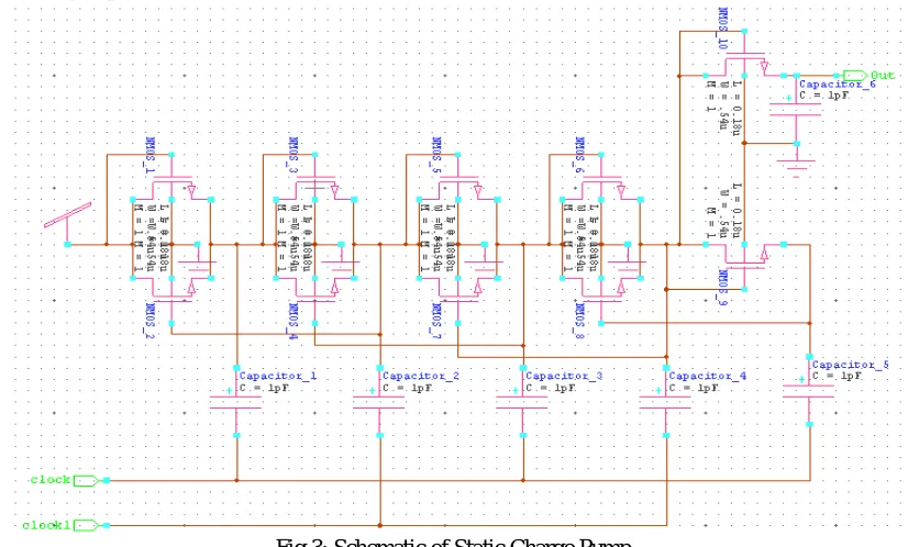
Static charge pump
The diode voltage drop i.e. Threshold voltage is removed by using charge transfer switch (CTS) in parallel with the diode connected device (MOS transistor) in order to improve the performance in low voltage applications. Therefore Static and dynamic CTS techniques have been found. CTS are used rather than the diodes to transfer the charge between nodes. Though the diodes are used only for setting up the initial voltage at each pumping node. The schematic of Static charge pump is shown in fig 3.
Fig 3: Schematic of Static Charge Pump
Static CTS technique uses higher voltage from the next stage for controlling the operation of the CTS’s. The functional workings of static charge pump as follows:
Case I: When the Clock is high and clock1 is low
Then NMOS_2 transistor is switched ON. Thereby initial voltage is setup at node2. The gate to source voltage of
NMOS_4 is 2∆ . If this gate to source voltage is greater than the threshold voltage of the NMOS_4. If this condition is
satisfied, NMOS_4 is turned ON.
Case II: When the Clock is low and clock1 is high
Then NMOS_3 will be switched off. Therefore gate to source voltage of NMOS_4 is 2∆ . There is such a condition
which occurs i.e. 2∆ < , where Vtn is the threshold voltage of MOS transistor. Therefore NMOS_4 will be switched
off, which is not valid. Thus performance of this charge pump is decreased.
II. RESULT, ANALYSIS AND COMPARISON
In this analysis here we show that the Simulation results of all implemented different types of charge pump. Function of designs is verified by using simulation based verification. This verification guarantee that the design is functionally correct when tested with given inputs. Designed charge pump have been implemented and simulated on Tanner tool in 180nm technology.
Dickson charge pump
The diode-connected NMOS transistors are used in the Dickson charge pump rather than the diodes for implementing the circuit in standard CMOS process. The diode connected NMOS transistor permit the charge flow only in the direction of the output stage in ideal situation. The charges are pushed to the next from one stage, resulting in higher DC voltage at the output.
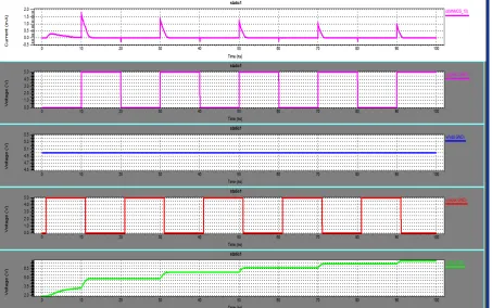
The simulation of Dickson charge pump is done at 180nm technology and W/L ratio = 540/180 of NMOS transistor and output waveform is shown in fig: 4.
Fig 4: Output Wave Form of Dickson Charge Pump
Voltage analysis of the Dickson charge pump is obtained at different VDD, constant VDD, same Vdd, same clock pulse,
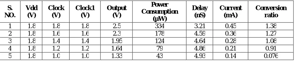
Table 1: Output Voltage, Power Consumption, delay, current and conversion ratio at different Vdd and same clock pulse of Dickson S. NO. Vdd (V) Clock (V) Clock1 (V) Output (V) Power Consumption (µW) Delay (nS) Current (mA) Conversion ratio
1 5 5 5 9.5 334 1.77 1.5 1.9
2 1.8 1.8 1.8 2.5 267 3.21 0.45 1.38
3 1.6 1.8 1.8 2.5 232 3.8 0.45 1.56
4 1.4 1.8 1.8 2.42 225 4.26 0.45 1.72
5 1.2 1.8 1.8 2.34 217 4.7 0.45 1.95
6 1 1.8 1.8 2.27 209 5.08 0.45 2.27
Table 2: Output Voltage, Power Consumption, delay, current and conversion ratio at same Vdd & different clocks pulse of Dickson S. NO. Vdd (V) Clock (V) Clock1 (V) Output (V) Power Consumption (µW) Delay (nS) Current (mA) Conversion ratio
1 1.8 1.8 1.8 2.5 334 3.21 0.45 1.38
2 1.8 1.6 1.6 2.3 178 4.59 0.36 1.27
3 1.8 1.4 1.4 1.95 124 4.64 0.28 1.08
4 1.8 1.2 1.2 1.64 79 4.86 0.21 0.91
5 1.8 1.0 1.0 1.33 43 4.93 0.14 0.076
Table 3: Output Voltage, Power Consumption, and delay, current conversion ratio at same Vdd, same clock & different clock1 pulse of Dickson
S. NO. Vdd (V) Clock (V) Clock1 (V) Output (V) Power Consumption (µW) Delay (nS) Current (mA) Conversion ratio
1 1.8 1.8 1.8 2.5 334 3.21 .45 1.38
2 1.8 1.8 1.6 2.5 206 3.25 .25 1.38
3 1.8 1.8 1.4 2.4 174 3.56 .22 1.33
4 1.8 1.8 1.2 2.2 145 3.8 .18 1.22
5 1.8 1.8 1.0 2.1 118 4.33 .15 1.11
Static charge pump
Static charge pump uses CTS in addition to Dickson charge pump to remove the problem of voltage threshold drop. Static CTS charge pump employing dynamic switches to increase the voltage pumping gain. The vital idea behind these multipliers is to use MOS switches with accurate on/off characteristics to direct charge flow.
Fig 5output wave form of static charge pump
Voltage analysis of the Static charge pump is obtained at different VDD, constant VDD, same Vdd, same clock pulse,
different clock pulse and constant clock pulse. At same condition power consumption and delay, also obtained. On varying the input voltage change in output voltage is observed. Its different parameters such as output voltage, power consumption, delay, output current and voltage conversion ratio are calculated and listed below in table 4,5,6.
Table 4: Output Voltage, Power Consumption, delay and current at different Vdd and same clock pulse of Static
S. NO.
Vdd (V)
Clock (V)
Clock1 (V)
Output (V)
Power Consumption
(µW)
Delay (nS)
Current (mA)
Conversion ratio
1 5.0 5.0 5.0 7.88 402 .94 1.8 1.57
2 1.8 1.8 1.8 2.6 397 1.4 .66 1.44
3 1.6 1.8 1.8 2.5 381 1.5 .65 1.56
4 1.4 1.8 1.8 2.4 370 1.52 .65 1.71
5 1.2 1.8 1.8 2.23 362 1.74 .64 1.85
Table 5. Output Voltage, Power Consumption, delay and current at same Vdd & different clocks pulse of Static S. NO. Vdd (V) Clock (V) Clock1 (V) Output (V) Power Consumption (µW) Delay (nS) Current (mA) Conversion ratio
1 1.8 1.8 1.8 2.6 402 1.4 .66 1.44
2 1.8 1.6 1.6 2.36 320 1.67 .56 1.31
3 1.8 1.4 1.4 2.13 242 1.92 .45 1.18
4 1.8 1.2 1.2 1.8 167 2.22 .32 1.00
5 1.8 1 1 1.36 81 4.66 .20 0.75
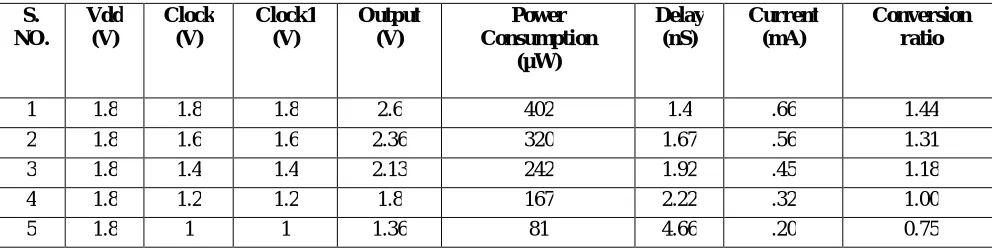
Table 6 . Output Voltage, Power Consumption, delay and current at same Vdd, same clock & different clock1 pulse of Static S. NO. Vdd (V) Clock (V) Clock1 (V) Output (V) Power Consumption (µW) Delay (nS) Current (mA) Conversion ratio
1 1.8 1.8 1.8 2.6 402 1.4 .66 1.44
2 1.8 1.8 1.6 2.47 366 2.19 .58 1.37
3 1.8 1.8 1.4 2.33 331 2.44 .50 1.29
4 1.8 1.8 1.2 2.18 296 2.61 .42 1.21
5 1.8 1.8 1.0 2.01 262 3.16 .34 1.11
III. CONCLUSION
From the above results, we have seen that various parameters are such as output voltage, power consumption, delay, output current and conversion ratio are analyzed for different types of charge pump with respect to power supply voltage.
Comparison result of output voltage shows that the charge pump with cross connected NMOS cells is best rather than
other charge pump which is a 5.77V at 1.8 power supply voltage.
Comparison result of power consumption shows that the Dickson charge pump is best rather than other charge pump
which is a 267µW at 1.8 power supply voltage.
Comparison result of delay shows that the charge pump with CTS Control Scheme is best rather than other charge pump which is a .04nS at 1.8 power supply voltage.
REFERENCES
[1]. P. Karuppanan, Kamran Khan and Soumya Ranjan Ghosh, “Dynamic gate and substrate control charge pump circuits”, Analog Integr
Circ Sig Process, springer, pp: 257–270, 2015
[2]. Jung-woong Park, Ho-yong Choi and Nam-soo Kim, “Two-stage feedback-looped charge-pump for spur reduction in CMOS PLL”,
Analog Integr Circ Sig Process, springer, Issue 2, vol :83, pp: 143-148, 2015
[3]. Huan peng, nghia tang, youngoo yang, member, , and deukhyoun heo, “CMOS startup charge pump with body bias and backward control for energy harvesting step-up converters” IEEE transactions on circuits and system, vol. 61, no. 6, june 2014
[4]. Oi-Ying Wong, Hei Wong, Wing-Shan Tam, Chi-Wah Kok, “On the design of power- and area-efficient Dickson charge pump circuits”, Analog Integr Circ Sig Process, springer, pp: 373-389, 2014
[5]. Yuh-Shyan Hwang, An Liu, Chia-Hsuan Chen, Yi-Tsen Ku, Jiann-Jong Chen and Cheng-Chieh Yu, “A continuous conduction mode low-ripple high-efficiency charge-pump boost converter” Analog Integr Circ Sig Process, springer, pp: 355-369, 2014
[7]. Yousr Ismail and Chih-Kong Ken Yang, “A 12-V Charge Pump-Based Square Wave Driver in 65-nm CMOS Technology” IEEE Asian
Solid-State Circuits Conference, pp: 237-240, 2014.
[8]. Alam siddique, Ferdous and Islam, “Charge pump capacitor based high voltage gain DC-DC step-up converter” IEEE, International
Conference Informatics Electronics & Vision (ICIEV),pp:1-4,2014.
[9]. Yang Lin, Wei-Chang Li, and Clark T.-C. Nguyen, “A MEMS-Based Charge Pump” Symposium on VLSI Technology, IEEE, pp: 148-149, 2013.