University of Windsor University of Windsor
Scholarship at UWindsor
Scholarship at UWindsor
Electronic Theses and Dissertations Theses, Dissertations, and Major Papers
2009
Design and Evaluation of a Parameterizable NoC Router for
Design and Evaluation of a Parameterizable NoC Router for
FPGAs
FPGAs
Michael Brugge
University of Windsor
Follow this and additional works at: https://scholar.uwindsor.ca/etd
Recommended Citation Recommended Citation
Brugge, Michael, "Design and Evaluation of a Parameterizable NoC Router for FPGAs" (2009). Electronic Theses and Dissertations. 115.
https://scholar.uwindsor.ca/etd/115
This online database contains the full-text of PhD dissertations and Masters’ theses of University of Windsor students from 1954 forward. These documents are made available for personal study and research purposes only, in accordance with the Canadian Copyright Act and the Creative Commons license—CC BY-NC-ND (Attribution, Non-Commercial, No Derivative Works). Under this license, works must always be attributed to the copyright holder (original author), cannot be used for any commercial purposes, and may not be altered. Any other use would require the permission of the copyright holder. Students may inquire about withdrawing their dissertation and/or thesis from this database. For additional inquiries, please contact the repository administrator via email
Design
&
Evaluation
of
a
Parameterizable
NoC
Router
for
FPGAs
By
Mike Brugge
A Thesis
Submitted to the Faculty of Graduate Studies Through Electrical and Computer Engineering In Partial Fulfillment of the Requirements for the
Degree of Master of Applied Science at the University of Windsor
© 2009 Mike Brugge
All Rights Reserved. No Part of this document may be reproduced, stored or otherwise retained in a retrieval system or transmitted in any form, on any medium by any means
Design & Evaluation of a Parameterizable NoC Router for FPGAs By
Mike Brugge
APPROVED BY:
N. Zamani
Mechanical, Automotive, and Materials Engineering
K. Tepe
Electrical and Computer Engineering
M. A. S Khalid, Advisor Electrical and Computer Engineering
Mitra Mirhassani, Chair of Defense Electrical and Computer Engineering
iv
Author’s
Declaration
of
Originality
I hereby certify that I am the sole author of this thesis and that no part of this thesis has been published or submitted for publication.
I certify that, to the best of my knowledge, my thesis does not infringe upon anyone’s copyright nor violate any proprietary rights and that any ideas, techniques, quotations, or any other material from the work of other people included in my thesis, published or otherwise, are fully acknowledged in accordance with the standard referencing practices. Furthermore, to the extent that I have included copyrighted material that surpasses the bounds of fair dealing within the meaning of the Canada Copyright Act, I certify that I have obtained a written permission from the copyright owner(s) to include such material(s) in my thesis and have included copies of such copyright clearances to my appendix.
v
Abstract
The Network-on-Chip (NoC) approach for designing (System-on-Chip) SoCs is currently emerging as an advanced concept for overcoming the scalability and efficiency problems of traditional on-chip interconnection schemes. This thesis addresses the design and evaluation of a parameterizable NoC router for FPGAs. The importance of low area overhead for NoC components is crucial in FPGAs, which have fixed logic and routing resources. We achieve a low area router design through optimizations in switching fabric and dual purpose buffer/connection signals. We propose a component library to increase re-use and allow tailoring of parameters for application specific NoCs of various sizes. A set of experiments were conducted to explore the design space of the proposed NoC router using different values of key router parameters: channel width (flit size), arbitration scheme and IP-core-to-router mapping strategy. Area and latency results from the experiments are presented and analyzed.
vi
Acknowledgements
I would like to express my sincere gratitude to my supervisor, Dr. Mohammed A. S. Khalid, where my research would not be possible without his advice and wisdom that guided me over the course of this research. I first met Dr. Khalid during the third year of my undergraduate degree, when he taught a class in digital system design. He stimulated my interest in this field. Although this class was based on processor design, he also provided an introduction into VHDL and embedded system design. The next year, I was able to get into his embedded system design class where I developed my skills and received excellent experience in the exciting field of reconfigurable computing. For this very reason, it had motivated me to continue my academic career in this field. My appreciation also goes out to my thesis committee members, Dr. K. Tepe and Dr. N. Zamani, for their time to sit on my committee and for reviewing my thesis.
I want to thank my family for all their constant support and encouragement. Thanks to my parents for their understanding throughout. Thanks for helping to keep me focused day after day. Thanks to my brother Shawn for providing some less stressful activities such as movies and Spitfire games. Thanks to my girlfriend Amy for always listening and helping me work through any and all problems.
vii
Table
of
Contents
Author’s Declaration of Originality ... iv
Abstract ... v
Acknowledgements ... vi
List of Figures ... xi
List of Tables ... xiii
List of Abbreviations ... xiv
1. Introduction ... 1
1.1 Thesis Objectives ... 4
1.2 Thesis Organization ... 4
2. Background and Previous Work ... 5
2.1 Overview of NoC ... 5
2.1.1 NoC Building Blocks ... 5
2.1.1.1 Links ... 6
2.1.1.2 Network Interface ... 6
2.1.1.3 Routing Node ... 6
2.1.2 NoC Parameters ... 7
2.1.2.1 Infrastructure ... 7
viii
2.1.2.1.2 Topology ... 7
2.1.2.1.3 Buffering ... 9
2.1.2.1.4 Floor Planning ... 9
2.1.2.2 Communication Mechanism ... 9
2.1.2.2.1 Flow Control ... 9
2.1.2.2.2 Switching Mode ... 10
2.1.2.2.3 Switching Mechanism ... 10
2.1.2.2.4 Routing Algorithm ... 11
2.1.2.3 Mapping ... 11
2.1.2.3.1 Scheduling ... 11
2.1.2.3.2 Module Mapping ... 11
2.1.3 NoC Evaluation Metrics ... 11
2.1.3.1 Latency/Throughput ... 12
2.1.3.2 Area ... 13
2.1.3.3 Energy/Power Consumption ... 13
2.1.3.4 Quality of Service (QoS) ... 13
2.1.3.5 Flexibility ... 14
2.2 FPGA Technology ... 14
2.3 Related Work ... 17
2.4 Summary ... 22
3. A Parameterizable NoC Router Architecture ... 23
3.1 Functionality ... 23
3.1.1 Protocols and Algorithms ... 23
3.1.1.1 Flow Control ... 24
3.1.1.2 Switching Mode ... 24
3.1.1.3 Routing Algorithm ... 24
3.1.1.4 Scheduling ... 26
3.2 Router Implementation ... 27
ix
3.2.2 Input Channel ... 29
3.2.2.1 Input Buffer ... 30
3.2.2.2 Input Controller ... 31
3.2.3 Switching Mechanism... 31
3.2.4 Output Channel ... 31
3.2.4.1 Output Buffer ... 32
3.2.4.2 Output Controller ... 33
3.3 NoC Architecture ... 33
3.3.1 Data Transfer between Routers... 33
3.3.2 Building a NoC Network ... 36
3.4 Verification ... 38
3.5 Summary ... 39
4. Experimental Evaluation results ... 40
4.1 Design Methodology ... 40
4.2 Synthesis Results ... 40
4.2.1 Arbitration ... 42
4.2.2 Flit Size ... 44
4.2.3 Configuration ... 45
4.3 Router Performance ... 47
4.4 Experimental Evaluation Framework ... 49
4.4.1 Arbitration ... 50
4.4.2 Flit Size ... 50
4.4.3 Configuration ... 50
4.5 Experimental Results and Analysis ... 52
4.5.1 Arbitration ... 53
4.5.2 Flit Size ... 55
4.5.3 Configuration ... 57
4.6 Summary ... 59
5. Conclusions and Future Work ... 60
x
5.2 Future Work ... 61
Appendix A ... 63
Detailed Synthesis Results ... 63
References ... 69
xi
List
of
Figures
Figure 2.1: Illustration of Four Basic NoC Building Blocks [23] ... 6
Figure 2.2: Popular NoC Topologies [3] ... 8
Figure 2.3: FPGA Architecture [25] ... 15
Figure 2.4: Altera Logic Element Architecture [26] ... 16
Figure 2.5: Xilinx Slice Architecture [26] ... 16
Figure 2.6: Four Input LUT [25] ... 17
Figure 3.1: Coordinate Configuration for XY Routing ... 25
Figure 3.2: Configuration of Local Ports for XY Routing ... 26
Figure 3.3: Architecture of Port: I/O Channels and Switch ... 28
Figure 3.4: Handshake Scenario between I/O Ports ... 29
Figure 3.5: Architecture of Input Buffer ... 30
Figure 3.6: Architecture of Input Controller ... 30
Figure 3.7: Architecture of Switching Fabric ... 32
Figure 3.8: Architecture of Output Buffer ... 32
Figure 3.9: Architecture of Output Controller ... 33
Figure 3.10: Architecture of Proposed Router ... 34
Figure 3.11: Connections between Adjacent Routers ... 35
Figure 3.12: NoC Router Design Flow ... 36
Figure 3.13: East to North Transfer Simulation Output in Altera Quartus II CAD tool ... 39
Figure 4.1: Proposed NoC Router Design Space ... 49
Figure 4.2: Single Router Architecture ... 51
xii
Figure 4.4: 2X2 Mesh Architecture a) Map 1 b) Map 2 ... 52
Figure 4.5: Effect of Arbiter Choice on Throughput ... 54
Figure 4.6: Effect of Arbiter Type on FPGA Area Utilization ... 54
Figure 4.7: Effect of Flit Size on Throughput for Test 1 ... 56
Figure 4.8: Effect of Flit Size on Throughput for Test 2 ... 56
Figure 4.9: Effect on Flit Size on FPGA Area Utilization ... 57
Figure 4.10: Effect of Configuration on Throughput ... 58
xiii
List
of
Tables
Table 2.1: Related Work ... 18
Table 3.1: Coding Scheme for Different Arbiters ... 37
Table 4.1: Area Utilization for Router Components ... 41
Table 4.2: Area Utilization for LiPaRs Router Components ... 42
Table 4.3: Effect of Arbiter Choice on FPGA Utilization, Optimized for Area ... 42
Table 4.4: Effect of Arbiter Choice on FPGA Utilization, Optimized for Speed ... 43
Table 4.5: Effect of Flit Size on FPGA Utilization, Optimized for Area ... 44
Table 4.6: Effect of Flit Size on FPGA Utilization, Optimized for Speed ... 45
Table 4.7: Effect of Configuration on FPGA Utilization, Optimized for Area ... 46
Table 4.8: Effect of Configuration on FPGA Utilization, Optimized for Speed ... 46
Table 4.9: Effect of Configuration on Routing Resource Utilization ... 47
Table 4.10: Simulation Results for Arbitration ... 53
Table 4.11: Simulation Results for Flit Size ... 55
xiv
List
of
Abbreviations
Abbreviation Definition_________________________________________________ ASIC Application Specific Integrated Chip
BRAM Block Random Access Memory CAD Computer Aided Design
CPU Central Processing Unit CS Circuit Switched
DSP Digital Signal Processing deMUX De-Multiplexer
FIFO First In / First Out Flit Flow Control Unit
FPGA Field Programmable Gate Array FSM Finite State machine
HLP High Level Protocol HOL Head-Of-Line I/O Input / Output IC Integrated Circuit IOB I/O Block
IP Intellectual Property LE Logic Element LUT Lookup Table
xv NEP Signal (Non-Existent Port) NoC Network-on-Chip
NRE Non-Recurring Engineering PS Packet Switched
QoS Quality of Service RRA Round Robin Arbiter SAF Store and Forward SoC System-on-Chip VCT Virtual Cut-Through
1
Chapter
1
Introduction
1. Introduction
The complexity of a system on silicon is comparable to other macro systems such as space shuttle or skyscrapers, when measured in terms of the number of basic elements intricately connected together, but at a micro level [22]. Moore’s law describes an important trend in the history of the integrated circuit (IC): the number of transistors that can be placed on an IC is increasing exponentially, doubling approximately every two years. This trend has continued for more than half a century. Increasing transistor density, higher operating frequencies, shorter time-to-market and reduced product life cycle, characterize today's semiconductor industry. As semiconductor technology evolves, electronic industries continually push the envelope for greater functional and performance capabilities in new electronic systems. This is creating a continuing need for new design methodologies and design space exploration.
2
hardware and/or software blocks, such as processors, DSPs, memories, peripheral controllers, gateways, and other custom logic blocks.
The communication architecture implemented in SoCs is an important contribution to the overall performance. Since the introduction of SoC concept, designers relied on a custom-designed ad-hoc mixture of buses and dedicated wires as communication mechanisms. Dedicated wires are effective for systems with a small number of cores, but available routing resources are quickly used up as system complexity grows. They also provide poor reusability and flexibility. A shared bus is a set of wires common to multiple cores, which increases both reusability and scalability. This scheme works well for Master-Slave communication patterns, where peripherals (slaves) wait for data to be received or requested from a more complex processing IP core (master). However, when there are several masters in the system, contention creates a bottleneck which gets worse as complexity grows. And although using hierarchical bus models separated by bridges may reduce some of these constraints, it also complicates protocols while failing to fully eliminate the scalability problem. Design and verification times also grow with SoC complexity [13].
3
and locked buses) for FPGAs. There is a great need for research in hardware implementation of NoC systems to determine the feasibility of implementing various parameters, and also to accurately determine what design tradeoffs are involved in NoC implementation.
ASICs are increasingly being replaced by Field Programmable Gate Arrays (FPGAs) for applications with low to medium volume, due to longer design cycles and high cost [14]. FPGA's have also continued to grow with the increase in chip density. Modern FPGA's have various hardware and/or software blocks embedded within them, such as DSP blocks, memory, and even processors. These blocks, along with customizable logic blocks, makes them the perfect candidate for NoC designs. A fundamental difference between ASICs and FPGAs is that wires in ASICs are designed such that they match the requirements of a particular design. Wire parameters such as length, width, layout and the number of wires can be varied to implement a desired circuit. Conversely, in an FPGA, area is fixed and routing resources exist whether or not they are used. The electrical characteristics of the FPGA are solved by the chip vendor, not by the user [3]. Exploiting the advantages of NoC in FPGAs for implementing SoC designs is an active area of research where the goal becomes implementing a circuit within the limits of available resources. Hence, the importance of designing a generic light-weight router whose area can be traded-off for performance in many different ways, to meet applications requirements.
4
1.1
Thesis
Objectives
The main goal of this research was to evaluate NoC router parameters based on area and latency to allow designers to make informed choices for the creation of large embedded systems on FPGAs. This research has the following major objectives:
1. Investigate the feasibility of NoC router implementation on FPGAs.
2. Explore the effects of varying NoC router parameters on area and latency. To date, not much research has been done to address this issue.
3. Investigate and design benchmarks with features that would severely test the NoC router implementations.
For the first objective, an experimental framework was developed using VHDL, allowing synthesis in Altera Quartus II CAD tool design environment. A parameterizable NoC router was designed and tested. Literature survey was conducted that showed a lack of results on NoC router implementation for FPGAs. Parameters that were not explored in previous research were selected and design space exploration was conducted for different values of those parameters. To address the third objective, benchmarks for each parameter were developed based on application and random traffic patterns. Finally, the proposed router was experimentally evaluated, using different parameter values, based on metrics such as area, latency, throughput, FPGA on-chip memory utilization and FPGA routing resource utilization.
1.2
Thesis
Organization
5
Chapter
2
Background
and
Previous
Work
2. Background and Previous Work
In this chapter, the background and previous work that is relevant to this research is presented. This chapter begins with an overview of Network-on-Chip (NoC) and NoC parameters. That is followed by a section discussing NoC evaluation metrics. Next a section describing FPGA technology is presented. The chapter concludes with a discussion of previous work closely related to NoC router design and evaluation.
2.1
Overview
of
NoC
There are many research papers and books dealing with micro-networks, with many subtle differences in definitions, concepts, and theories. In this section, for the sake of clarity, we present a collection of concise definitions of relevant concepts and theory that holds true for most NoC systems including our proposed router architecture. Emphasis is placed on how such concepts relate to FPGA implementations wherever necessary.
2.1.1
NoC
Building
Blocks
6
Figure 2.1: Illustration of Four Basic NoC Building Blocks [23]
2.1.1.1
Links
This component provides connections for a routing node with a network interface or another routing node. It may provide buffer resources and separate control lines for connection establishment and teardown.
2.1.1.2
Network
Interface
This component provides the conversion between the high level protocol (HLP) that the IP uses and the packet-based communication protocol of the NoC. This component may be responsible for buffering packets, storing IP core addresses, creating and disassembling messages, implementing end-to-end flow control, crossing clock domains, and other higher level network issues.
2.1.1.3
Routing
Node
7
which are all focused around router design. Research in this area still lacks in useful implementation results.
2.1.2
NoC
Parameters
Network parameters are an important research topic among NoC designers. To further enhance performance, the parameters of the NoC should be chosen based on the specific application. Therefore, the goal in a general network design is to leave as much designer flexibility as possible. Not every network parameter can be created flexible and many of the parameters are dependent on each other. Evaluation and testing can provide insight into how to select these parameters, although a better solution may be a flexible library of interchangeable components. We have chosen to create such a library using VHDL, and use an FPGA to provide fast prototyping for results. Due to time and resource constraints, limitations had to be set on the amount of design space explored. Network parameters can be broken into three groups as in [2]: Infrastructure, Communication Mechanism, and Mapping. Each of these groups will be discussed separately below.
2.1.2.1
Infrastructure
Infrastructure aims to determine the network architecture and includes channel width, topology, buffering and floor planning. These parameters are all application specific and should be left to the designer’s discretion.
2.1.2.1.1
Channel
Width
This parameter describes the size of the data passed between routers. It is important since it directly affects bandwidth but can lead to the side affects of increased area/power. Our library allows for a parameterizable channel width which will also be tested for resulting area and latency tradeoffs.
2.1.2.1.2
Topology
8
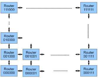
Saldana et al. evaluate different topologies in terms of area and routing resources [3]. Figure 2.2 shows some popular NoC topologies. Ring and star achieve slightly better results, although both fail to provide solutions to the scalability problem. As the number of nodes increases, ring suffers large end to end delay and star suffers from a central bottleneck. Narasimhan et al. compare the performance of a two dimensional torus to mesh, showing a slight edge for two dimensional torus [4]. They however, do not compare the extra routing resources needed or the increase area of each router due to a more complex routing algorithm. We restrict the topology to mesh, which is most common among FPGA networks, but allow for various implementation sizes up to an 8 x 8 network. We also create multiple local ports (up to four per router), which allows for multiple IP cores connected to each router or multiple router connections for single IP cores. This increases the possible number of IP cores connected in the network from 64 to 256. With available FPGAs, it would be impractical to build anything larger due to area and routing resource constraints.
9
2.1.2.1.3
Buffering
This parameter defines the approach used to store messages while they cannot be scheduled. This has a serious impact on the area overhead of the network, however, it can also have a serious impact in reducing network latency. We use input and output buffering to prevent head-of-line blocking (HOL). This occurs when a packet or packets, experience blocking and cause the blocking of later packets which could otherwise be processed. The inclusion of an output buffer allows the blocked packet to move out of the input buffer, to unblock the later packets for processing. Buffer allocation should be based on traffic patterns. The authors of Hermes [8] design a generic router which has a parameterizable buffer depth. They also include insight through testing various buffer sizes for area and performance values.
2.1.2.1.4
Floor
Planning
Floor planning involves the placement of network components. This is not important in FPGA-based NoC designs as it is done by vendor specific CAD tools (Altera Quartus II CAD tool).
2.1.2.2
Communication
Mechanism
Communication mechanism deals with how data flows through the network and includes flow control, switching mode, switching mechanism, and routing algorithm. These parameters are usually set when designing the NoC platform.
2.1.2.2.1
Flow
Control
10
guaranteed bandwidth during connection times. This method does not scale as well and is not a popular choice for NoC systems. In packet switching, data is broken into packets which carry routing information. Packets can further be broken down into flow control units (flits). Modules can send packets at any time and there are often many different packets in flight at a given time. The routers must process and redirect each packet accordingly.
2.1.2.2.2
Switching
Mode
This parameter only exists in PS networks and defines how packets move through the network. The most important schemes are store-and-forward (SAF), virtual cut-through (VCT), and wormhole (WH). In SAF, a router cannot forward a packet until all its flits have been received. Therefore, latency is proportional to packet size and it carries large buffer requirements. In WH, the first flit (header) determines the next hop and all remaining flits follow and can be sent as soon as it’s received. Therefore, latency is proportional to flit size. This method combines packet switched flow control with circuit switched ideas but also leads to channel reservation. It also requires a complex routing algorithm. VCT uses a combination of both ideas to provide latency based on flit size without idle times by guaranteeing buffering before setting up the connection. However, this method uses large buffer amounts and very complex routing algorithms making it unsuitable for light-weight networks. We have chosen SAF for its light-weight algorithm and to prevent channel reservation. Future testing may extend flexibility to include WH as well.
2.1.2.2.3
Switching
Mechanism
11
2.1.2.2.4
Routing
Algorithm
The routing algorithm determines the path the packet will take. There is not much research guidance available on effectiveness of available routing algorithms for NoC implementations. We use XY routing for its simplicity and low area overhead. This scheme also prevents livelock and assures flits and packets arrive in order. Routing schemes can also require congestion control and recovery mechanisms, which can lead to added area overhead. We allow this to be handled by the application layer.
2.1.2.3
Mapping
Mapping determines how to integrate a given application to the NoC platform and includes scheduling and module mapping.
2.1.2.3.1
Scheduling
This is a traditional computer science topic but most work neglects inter-processor communication. Arbitration schemes consider priority of packets when making grants inside the routers among the network. Arbiter schemes can be static or dynamic. Dynamic arbitration makes a decision at run-time and is more flexible, however also requires a larger area. Dynamic Schemes can also prevent starvation which is a downfall of static schemes. Our library provides a few different components to allow for area and latency trade-offs.
2.1.2.3.2
Module
Mapping
This parameter aims at selecting IP modules for different locations to minimize traffic. This parameter is application specific and is explored later.
2.1.3
NoC
Evaluation
Metrics
12
improved at the cost of other(s). In the following sections we will discuss the evaluation metrics for NoC router architectures and their relevance to this thesis.
2.1.3.1
Latency/Throughput
When using FPGA technologies, evaluating speed can often be as easy as obtaining the synthesized maximum frequency the clock is capable of running at. For NoC routers, this is not the case. Although still important to the overall performance, NoC routers have multiple ports which can send, receive and process simultaneously. Therefore, it is important to observe data transaction times.
Speed can be measured in delay, which is referred to as latency. Latency can be the overall run time, it can be decomposed into several intervals such as packet or flit latency, calculated as an average, along with other creative possibilities. We use the overall application run time measured in cycles, which is converted to time as a function of the maximum clock frequency.
Speed can also be measured in bandwidth, which is referred to as throughput. Throughput is the amount data transferred over a period of time. Throughput can be; the ideal data processing rate (system working under the best possible conditions), it can be decomposed into several intervals such as overall application, packet or flit throughput, measured per system, IP core, router, or port, calculated as an average, along with other creative possibilities. We use the overall application/simulation throughput measured in packet and flits per cycle, which is converted to time as a function of the maximum clock frequency.
Finally, some papers suggest NoC router speed be measured in terms of bottlenecks. Either the number of occurring bottlenecks, or the time in which a router has a bottleneck occurring. This metric was not used in our experiments but is very interesting to note.
13
2.1.3.2
Area
In an FPGA, overall system area is limited and therefore important to keep minimal. Area can be measured as a number or a percent of available resources. Area is a very vague term. In an FPGA, there are many components which occupy area. For our experiments, we use area in terms of logic elements (LE’s), memory blocks, and routing resources (direct wires, interconnects, and clocks). This Information is obtained from Altera Quartus II CAD tool after compiling and synthesizing the VHDL code. Altera Quartus II CAD tool gives the option to synthesize for the lowest area or highest speed.
2.1.3.3
Energy/Power
Consumption
For FPGA technologies, power consumption is a metric not often evaluated. This is due to the fact that power consumption has a direct relation with area. Also, designing low power circuits for FPGA implementation is based on trial and error. Therefore, most research including ours focuses on area and excludes the use of power estimation tools.
2.1.3.4
Quality
of
Service
(QoS)
Quality-of-Service (QoS) is a networking term that refers to guarantees that the system can make about its performance. In computer networks, certain application such as video streaming are required to give a guarantee of high uninterrupted bandwidth because of the uniqueness of the application. It is difficult to actually predict the behavioral nature of the data in the network, thus making it nearly impossible to guarantee the required bandwidth without some margin of error. PS suffers even more in its ability to predict the timing of its services. To help provide QoS, NoCs must provide service free of the following causes of failure:
1. Livelock: data is prevented from reaching its destination because it is in a cyclic path.
14
3. Deadlock: data is prevented from reaching its destination because it is blocked at some intermediate resource.
Livelock occurs when the packets are being routed around their destination and are placed in a cyclic holding manner. Livelock can be avoided by allowing the packet to travel the shortest route. XY routing avoids this situation.
Starvation is a common PS problem. It occurs when the packet is discriminated against as low-priority data, thus never getting service. This can be avoided by allocating resources to process all packets equally, automatically dropping and resending packets in the network for too long, or by use of dynamic arbitration insuring all ports receive service.
Deadlock is cause by packet being continuously blocked and it is the hardest problem to solve because packets that are blocked stay blocked while waiting for an event that cannot happen. This problem is solved by restricting channel reservation.
2.1.3.5
Flexibility
Flexibility refers to the number of manipulations the designer can make. Our router design allows that some of the parameters be changed at design time allowing the designer to choose trade-offs. Designs with a high degree of flexibility are the ones that allow more parameters to be changed. Other flexibility characteristics include scalability (ability to add more and more IP cores) and design re-uses (ability to use the same NoC architecture for multiple designs).
2.2
FPGA
Technology
as st bi co sp sp co (A F co th
s block rand till provide s
its in mem onnections. peeds of tens
We c pecific integ onsume mo ASICs). The
PGA allow ompared to hrough repro
dom access m some degree mory cells w An FPGA c s of megaher
an use an F grated circuit ore area and
e use of FPG ws for faster
ASIC. The ogramming.
memories (B e of configu which contr can support rtz.
Figure 2.3
FPGA to im t (ASIC) cou d energy co GA to implem
r prototypin e main advan
15 BRAMs) and urability. An rol transisto
hundreds of
3: FPGA Arc
mplement an uld perform, ompared to ment digital ng, shorter t ntage comes
d digital sign n FPGA is p r switches f thousands
chitecture [2
ny logical f , however FP
application circuits is o time to ma s from the ab
nal processo programmed to establish of gates of l
5]
function tha PGAs tend t n-specific in n the rise ov arket, and lo
bility to fix
ors (DSPs) w d by loading h non-perm logic operati
at an applica to run slowe ntegrated cir ver ASIC des ower NRE bugs in the
In E re lo The tw ncorporated Element (LE)
eferred to as ook-up table
Fi
wo largest m [24]. The b ) and is show s a slice and
(LUT) whic
igure 2.4: Al
Figure 2.
manufacture basic buildin
wn in Figure is shown in ch is basical
16 ltera Logic E
5: Xilinx Sli
s of FPGAs ng block in a
e 2.4. The b n Figure 2.5.
ly a block of
Element Arc
ice Architec
s are Altera an Altera FP basic buildin The basic f programma hitecture [26 ture [26] Corporation PGA is refer ng block in a
building blo able memory
6]
n [20] and X rred to as a L a Xilinx FPG ock of the LE y and is show
17
Figure 2.6. The LUT consists of an array of 1-bit memories which implement a truth table connected to a multiplexed output pin. In short, a Xilinx slice is basically made up of 2 LEs. Altera Stratix II EP1540F1508C5 was selected as the target device for this research. This device contains 41, 250 LE’s and was chosen for its popularity and large output pin capability for synthesis of large designs.
Figure 2.6: Four Input LUT [25]
2.3
Related
Work
18
Table 2.1: Related Work
Testing type
and
results
no testing no testing
simulat e s 5 x 5 net wor k with different buffer s izes
, latency dec
reas e for larg er buff e rs (pe rha ps d u e to central bottlene ck) 4 microbla z e, maste r/sla ve appli c ation with sh are d a nd local memory
, 32-bit bus
vs . 32-bit router Perform a nce fe at u res 40MHz cl k 50MHz cl k 25MHz cl k 55.8-6 6 M H z clk FPGA ar ea synthesis re sults 611 sli c e s 552 sli c e s 5-po rt/8-bit 2 7 8 slices 5-po rt/8-bit In put buffer depth 2 460-570 LE' s
depth 4 48
6-795
LE's
Area
s to imp
rove upon 1-D route r co nfiguratio n leadin g to sa me bottlene ck p roblem large routin
g table logi
c,
s
e
tup time, poss
ible
blockin
g
due
to VCT flow
control, witho u t remo ving buffer re quire ments arbitration an d routing logic i s ce ntra lized cre a ting requ est bot tl ene ck a n d rest rict in g simultan eou s conn ectio n possibilities vari ou s pa cket lengths lead
s to 2 ext
ra framin
g
bits in ea
ch flit and
compl e x routi ng logi c (upd ates h e a
der at ea
ch node ) Novel, use fu l featur es firs t work
ing implementation on
FPGA imp rov es u pon n e tw o rk stru cture allo wing 2 -D i rre gular topolog y simplifie s ro uting logi c, pro v ide s para m eteri z a b
le data wi
dth and
buffer depth, l
a ter wo rk prod uces CA
D tool for aut
o gene ration a n d eve n traffic anal ysi s (late n cy) decentrali ze d routing an d arbitration log ic, con c lu sio n of s h or te r ne tw or k w ir e s le ad in g to highe r clo c k frequ en cie s then in buses. Na me,
Author, year published, refer
e
nc
e []
N/A,
Marescaux, 2002, [6] N/A, Bartic
,
2003, [7] Her
m
e
s
,
Moraes,
2004, [8][9] RASoC, Zeferino,
2004, [10][11]
19 Testing type and results image bin a ri zation appli c ation co ntrolled b y microbla z e, 8 block in
total, 1 router vs. sh
ared and lo cked b u s simulate
s 1, 1x2, 3
x 3 route r co nfigu ration s
with without block
ing and with worst case blockin g , take s 24 cy cle s t o pro c es s 8-f lit packet simulat io n re st ri ct ed t o
SAF, RRA, 4 flit pac
k e ts , 36 nod es, re sults sa w
the CAD tool
signifi
cantl
y
redu
ce area
for lower injection rates simulate
s a 3
x 3 net work by imple m ent ing a wra ppe
r to inj
e ct pac ket s at va riou s rat e s and re po rts a v erage latenci e s Perform a nce fe at u res 138-151 Mh z clk 33.3MHz clk 107 MHz clk 286M Hz clk
(common) 357M
Hz clk
(multiple clk domain
s ) eliminate pa d dela y s FPGA ar ea synthesis re sults
8-bit 4-port 2
4 9 slices 8 -po rt 1113 slices (not including RA M for routing tabl e) 5-po rt/8-bit 352-432 slice s
5-port/8-bit (4 flit buffers) 23
0 slice s extre m e case => all ports sha ri ng output logi c 8 8 slices 5-po rt/8-bit 2 8 2 Slices comm on cl k 5-po rt/8-bit 3 3 2 slices multipl e clk domain s Area
s to imp
rove upon CS create s setup and teardo wn late ncy, blocks cha nnel s du ri ng idle time, comple x routin g
logic reduces scal
ability large 5 x 5 cro s spoint matrix , dy namic sched uling? (worth the extra a re a ), sl ow cl ock
(due to la
rge requ est/g rant process time) fu lly co nne ct e d swit ch, only sup port s output buffering VCT create s setup a nd teardo wn late ncy, blocks cha nnel s du ri ng idle
time, while sti
ll using buffers, al so goe s ba ck
to central arbi
tration whi c h create s perfo rman ce bottlene cks Novel, use fu l featur es circuit-switch
ed flow control
pro v ide s gu aranteed throug hput, suppo rts an y cu stom topol ogy o r num be r of ports
Input and out
put buffers, dual
purp o se sig n a ls re du ce s logic, impro v e s cro s sbar b a sed on XY routing, p rop ose s MLP R idea, later work c reates ex haus tiv e
CAD tool for
mappin g IP's and cho o si ng net wor k si ze sup port s ra ng
e of routing,
swit chin g, an d arbitration algorith m s, e nable s re so urce s h ar in g to low e r ar ea w her e highe r ban
dwidth isn't nee
d
ed,
CAD tool de
ci
des
sha
ring
based on inj
e ction rate take s cro ssb ar re du ction (based
on XY routing
) idea furth
e r by desi gning cu stom ports Na me,
Author, year published, refer
e
nc
e []
PNoC, Hilton, 2005, [13]
LiPaR,
Sethuram
an,
2005, [14][15] Gno
C , V e st ias,
2006, [17] MoCres,
Jan
a
rtha
nan,
20
The first working implementation of FPGAs was presented by Marescaux et al. [6]. It has many faults mainly large size, and a one dimensional architecture which fails to provide a high degree of scalability. They extend their work in [7], allowing a more flexible architecture, but still suffering from large area overhead. They use VCT flow control which is now considered too area-intensive for FPGA platforms because of complex routing logic without eliminating any buffer constraints.
Moraes et al, present Hermes, a router with parameterizable data width and buffer depth. They perform simulations of a 5 x 5 mesh while varying buffer depth. They conclude with the notion that increased buffer size reduced latency, but only to a saturation point. Their design uses centralized arbitration and routing units, which decreases area but stalls performance as routing requests are queued to be handled one at a time. Their design also suffers from a very low clock speed. They later extend their work to provide an automatic router generation and traffic analyzer [9].
A comparable router, RASoC [10], was presented by Zeferino et al. The main difference being they use a WH flow control. Performance differences are yet to be compared and may be considered for future work as a WH downfall is that it reserves channels which can cause blocking. However, WH also requires complex routing logic as well as extra bits in the datapath for framing. They also used Altera to synthesis their 5-port, 8-bit router which occupies 486 LE's and has a clock frequency of approximately 57MHz. This area is quite large for a router whose buffers are limited to 4 per port.
PNoc, proposed by Hilton et al in [13], gives us a router with circuit switched flow control. They test their router against bus based approaches to show improvements. However, routing complexity grows as the number of ports, or number of routers increase and therefore reduces scalability. It also suffers typical CS setup and teardown latencies and possible blocked idle time.
21
these optimizations to the arbitration unit. They use a single 5x5 crossbar matrix for switching rather then 5 5x1 partial crossbars leading to a larger area. Their complex crossbar design results in a slower clock speed and increased area.
They later propose multi-local port routers (MLPR) in [15], which have the potential of improving area and performance metrics. However, the authors fail to provide any synthesis results to support their proposal. Another extension the authors propose is Optimap [16], an exhaustive CAD tool for mapping IP's and choosing network size.
Vestias et al. propose GNoC in [17], a generic router which supports a range of routing, switching and arbitration protocols. They create a tool for exploring the sharing of some decentralized components to reduce area that is based on the injection rate of ports. Unfortunately, they lock all protocols to certain values and do not explore them further. Their tool shows how they can save area when injection rates are low but does not test to see if performance is degraded.
MoCres, designed by Janarthanan et al. in [18], uses complex VCT flow control and attempts to reduce area by sacrificing area through centralizing components. They create multi-clock domain to enable high clock frequencies during transfers. Optimizations from XY routing in the crossbar matrix have been extended to the routing algorithm, and gave us the idea for a further arbitration unit extension. We have also used their idea of creating VHDL wrappers to simulate the stand-alone router or routing configurations to compare parameters.
22
utilization and performance values for the above network parameters to help future designers make accurate decisions for their computing needs.
2.4
Summary
23
Chapter
3
A
Parameterizable
NoC
Router
Architecture
3. A Parameterizable NoC Router Architecture
In this chapter a detailed description of our proposed NoC router architecture is presented. This chapter begins with a discussion of basic functionality of the NoC router based on protocols chosen. That is followed by a discussion of the NoC router architecture describing the main components used and the data flow. NoC design is presented next, including functionality and how to assemble. We briefly discuss how the NoC router architecture was verified using Altera Quartus II CAD tool and then conclude the chapter.
3.1
Functionality
In section 2.1 we discussed NoC router parameters and gave some insight into the choices we have made for our router design. In the following sections, we will discuss those parameters in which directly affect the functionality of the router which include protocols and algorithms.
3.1.1
Protocols
and
Algorithms
24
The following sections describe our protocol and algorithm choices to provide working knowledge of our NoC router. These parameters include flow control, switching mode, routing algorithm, and scheduling.
3.1.1.1
Flow
Control
We have chosen a packet switched flow control. In PS networks, data is separated into small blocks called packets at the core. This packet includes a header which has information about its destination. Upon creation of the packet, IP cores simply release the packet into the network where a series of interconnected routers forward the packet to its destination. PS is referred to as connectionless as there is no direct connection between communicating cores. This is an attractive choice as it allows multiple IP cores to communicate without contention.
3.1.1.2
Switching
Mode
Switching mode can often be confused with flow control as it plays a large part on the flow of the packet. Switching mode is only a parameter of PS networks. This parameter is in charge of allocating buffers and channels to the packet and deciding when it will receive service. A packet is broken down into flow control units (flits). We have chosen to break the packet into 8 flits. Each flit is the size of the channel. We have chosen a store & forward (SAF) scheme. In this scheme, packets are buffered at each router, and the router waits for the full packet to arrive before forwarding. This prevents a single packet from blocking more than one channel at a time. The downfall is that it increases the buffering requirements of each router. Testing this parameter would be great future work as there are a few other alternatives. However, designing a router with different switching modes is very complex and was omitted from the scope of this research.
3.1.1.3
Routing
Algorithm
25
occurring. Since all packets leaving the same source and headed for the same destination will travel the same path, it also prevents having to deal with complex scenarios like packet reordering. Unfortunately, using the same logic, XY routing cannot provide any type of congestion control.
Figure 3.1: Coordinate Configuration for XY Routing
In XY routing, each router is given a coordinate based on its position in the network. We restrict our mesh size to 8X8 and therefore our coordinate is 6 bits. The most significant 3 bits portrays the routers vertical displacement with 000 being the lowest (southern) router and 111 being the highest (northern) router. The least significant 3 bits portrays the routers horizontal displacement with 000 being the left most (western) router and 111 being the right most (eastern) router. Figure 3.1 shows router coordinate configuration within a mesh. A packet arrives at the router with an 8 bit header. This header contains the destination of the packet. The vertical displacement is checked first. If the destination is greater then the coordinate, the packet is forward north. If the destination is lesser then the coordinate, the packet is forward south. If the destination is equal to the coordinate, then its vertical displacement is ok. The same process then
………
………….…
…………
...
26
occurs for the horizontal displacement. Eventually, the packet arrives at the router with the proper coordinate. At this point the packet is at the proper port and must now be forwarded to the correct destination port. Since routers in our mesh can have up to 4 ports, the least significant 2 bits of the header are used to distinguish among local ports. Figure 3.2 shows the configuration of local ports within the router.
Figure 3.2: Configuration of Local Ports for XY Routing
An important note can be made about this algorithm. Since the vertical displacement is always found first, a packet coming in from the east or west ports must already be in its proper vertical position. Therefore, a packet coming in from the east or west ports cannot be forwarded north or south. This observation is exploited later to optimize the area selected components.
3.1.1.4
Scheduling
27
arbitration schemes that consider priority of packets in routers among the network and are classified into static and dynamic schemes.
In static arbitration schemes, the priority of each port is chosen during design. First, we use a generic fixed scheme where priority is given to the north first, and degrades clockwise. We use two other static arbiters, both based on the fixed scheme. Both schemes were designed during the evaluation phase. Custom scheme was designed based on the setup of the simulation. Custom each port scheme included a different fixed priority in each port based on the setup of the simulation.
Dynamic arbitration makes a decision at run-time and is more flexible, however also requires a larger area. However, dynamic schemes can avoid deadlock. We include 3 counting schemes and a coin passing scheme. The counting schemes all have similar area results, but their performance depends on the application. The first scheme gives priority to the port that has been busiest (sending the most requests). The Next scheme gives priority to the port that has been waiting the longest. Here, the arbitration unit counts cycles after a request has been received for all ports. The last counting scheme gives priority to the port that sends the least packets (opposite to the first scheme). Finally, in coin passing scheme, one input port is assigned the coin. The port assigned with the coin, has priority, until it has been granted. Then the coin is passed to the next port, clockwise. If the port with the coin is not making a request, the unit grants the request of the port closes to it, again clockwise. This scheme is much like round robin used in many FPGA NoC router implementations.
Scheduling is one of the parameters we wish to test. Interesting results may show static arbiters latency is quite reasonable considering its area savings. This is especially a concern in decentralized routers, where each port has its own control logic.
3.2
Router
Implementation
28
therefore and input port has the ability to forward to its own output port, although this situation could never occur. Figure 3.3 shows the port architecture and it’s interaction with the switch. Packet size has been set to a depth of 8. Flit size is parameterizable, with 8 bits being the smallest possible size for routing information purposes. Our implementation does not include High Level Protocols (HLP) but could easily be implemented on an application level. The router is decentralized meaning each port runs its own control logic and hence can request and set up concurrent connections. Below we will include details on inter-router data transfers, the I/O channels and the crossbar switch designs.
29
3.2.1
Data
Transfer
between
Input
and
Output
Ports
Communication between ports is established by use of a two-way handshake of request/grant signals. Figure 3.4 shows a handshake scenario between local and west ports. Upon packet arrival, local sends a request for west’s output port. Once local receives a grant from west it can drive its request line back to low and it is free to send the packet, one flit at a time. West will hold its grant line high until the full packet has been received. Any other ports which have high request lines to west, will keep them high until they also receive a grant.
Figure 3.4: Handshake Scenario between I/O Ports
3.2.2
Input
Channel
30
3.2.2.1
Input
Buffer
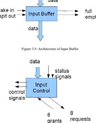
The input buffer is shown in Figure 3.5. It is capable of storing the whole 8 flits of the packet. It has 2 status signals letting the input controller know if it is full and ready to be forwarded or it is empty and ready to accept a new packet. It also has 2 control signals allowing the input controller to store or forward its contents.
Figure 3.5: Architecture of Input Buffer
31
3.2.2.2
Input
Controller
The input controller is shown in Figure 3.6. This unit is responsible for running the routing algorithm. It continually monitors the header flit and determines its next hop. When the buffer becomes full, the controller issues a grant to the appropriate output port. It then waits for the grant, when it can prompt the transfer. When the buffer becomes empty, the input controller can prompt transfers from the outside.
3.2.3
Switching
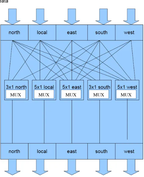
Mechanism
The crossbar switch is shown in Figure 3.7. It is a set of multiplexers having an interconnection allowing all possible connections between input and output channels. Three optimizations have been made in the crossbar switch. First, it uses a partial scheme, which includes one 5 by 1 unit for each output rather then one 5 by 5 unit for all outputs, for a 5 port router. Initial design included 2 switching options, full and partial switch. Early synthesis results eliminated the full switch design because it was larger in area and slower in clock frequency. Each output is connected to a different port. Next, there are no demultiplexers in the design. The input data is connected to all partial crossbar units which will choose the appropriate data for the output. The fact that at a time, the output channel can only serve one input request is exploited here. The final optimizations are made in the partial units of the north and south. Though analysis of the XY routing algorithm, we can conclude that these units will never receive data from the east or west. This reduces the inputs of all of these units by two. All optimizations reduce the area without effecting latency of the router.
3.2.4
Output
Channel
32
Figure 3.7: Architecture of Switching Fabric
3.2.4.1
Output
Buffer
The output buffer is shown in Figure 3.8. It is capable of storing the whole 8 flits of the packet. It has 2 status signals letting the output controller know if it is full and ready to be forwarded or it is empty and ready to accept a new packet. It also has 2 control signals allowing the output controller to store or forward its contents.
Figure 3.8: Architecture of Output Buffer
33
3.2.4.2
Output
Controller
The output controller is shown in Figure 3.9. This unit is responsible for running the arbitration algorithm and making grants. It continually monitors request line. When one or more become high, the controller issues a grant to the prioritized input port. It then waits for the packet, when it can prompt the transfer outside. When the buffer becomes empty, the output controller can continue issuing grants.
Figure 3.9: Architecture of Output Controller
3.3
NoC
Architecture
Although we propose the design of a stand-alone router with the purpose of testing its parameter, the router can of coarse be used in the building of a NoC network. The router protocols will only work for two dimensional mesh architecture, with properly positioned coordinates. The following sections discuss the intra-router data transfers, along with how to build a NoC using the proposed router and accompanying components.
3.3.1
Data
Transfer
between
Routers
34
transaction of data from a routers output port to the other routers input port. The output port will let the adjacent routers input port know when its buffer is empty, and therefore ready to receive a packet, through use of emptyout/emptyin signals. Once the output port has received a packet and the emptyin signal has been driven high by the adjacent router, it can begin sending. To start, it drives the sendingout signal high for just one clock cycle, which prepares the output port that all 8 flits will begin transferring upon the next clock cycle. When data begin to flow, the input port will send the emptyout signal to a low state, and stay that way until the packet has been forwarded within that specific router.
Figure 3.10: Architecture of Proposed Router
35
Figure 3.11: Connections between Adjacent Routers
Since are router provides a variable number of ports, and extra signal was added, NEP to make sure that there are no requests for a non-existent local port. This signal is driven high if the header of a packet requests a local port that is not included in that particular router. This signal is common on all routers and could be sent to a central processor (CPU), where it could stop the program and re-assess where the IP cores are in terms of NoC network position.
36
3.3.2
Building
a
NoC
Network
With our parameterizable router design, building a router takes careful placement of components. The design makes choices on channel width, number of local ports per router, and arbitration type. Also, when building a NoC, designers must configure the coordinates of each router based on its network position. Figure 3.12 shows a flowchart outlining how to build a NoC network. It is recommended to start with the lower left corner of the NoC and maintain a pattern when designing each router. This is to make integration of the coordinate a little easier.
Figure 3.12: NoC Router Design Flow
37
First is the choice of channel width. This cannot be made smaller then 8 bits for routing purposes. Once chosen, it must remain the same for all routers within the NoC network. This can be modified in the top level module by changing the generic parameter called flit size.
Next is the choice over how many local ports. Each router in the NoC network can have anywhere from 0 to 4 local ports independent of the other routers. This option is as simple as choosing the correct top level module for router design. Each top level router module is named after the number of local ports it has (router_fs_xx). Here the xx should be chosen to be 0l, 1l, 2l, 3l, or 4l implying the number of local ports each router has.
The final choice to be made is on which arbitration unit is to be used. The number of changes made here depends on the number of ports chosen. Each port must be opened separately, to change the name of the output controller used. Ports are named based on numbers (port_ns_x). Here the x is a number and is based on the number of ports in the design. So if you build a 6 port router, ports with numbers 0 to 5 should be opened and changed. Output controllers are named after their arbitration unit (outputcontrol_xx). Here the xx is replaced by select options listed in Table 3.1.
Table 3.1: Coding Scheme for Different Arbiters
Arbiter code Arbiter Type
fa Static – fixed scheme
c1, c2, c3 Dynamic – various counting schemes
cp Dynamic – coin passing (RRA) scheme
cap Static – custom application fixed scheme
ca0, ca1, ca2, ca3, ca4
38
Lastly, the router must be configured with its proper coordinates. Router positioning must be done carefully. Coordinates are configured in the input controller (inputcontrol) and are called router_coordinates.
Future re-design/improvements of this NoC router would see the use of corner routers which would eliminate the need for a couple ports further reducing area. Since we simply wish to test the parameters, this omission is fine. This reduction in area and power would be crucial for use of this router in a NoC system for real world implementation.
3.4
Verification
ModelSim [21] was used to create tests and obtain latency results, but before that phase testing on the routers functionality was needed. After choosing the parameters of the router, design began with the creation of components (buffers, controllers). As each component was finished, it needed to be tested for functionality. Each component would have to be verified before moving on in the design. There is no point in creating a router with components that do not work correctly. This phase was completed in Altera Quartus II CAD tool using the waveform editor and simulation tool. The output controller needed extra testing as the priority of each port needed to be tested for different arbiter types First each component was tested to ensure its control signals were working and data was flowing through the components with proper timing. Then came creation of a generic port composed of the components. Testing was done to ensure each port could receive and send data properly. Finally a 5-port router was designed. As it is nearly impossible to verify every possible bit stream scenario in a router, a few situations were simulated. First was a common transfer. The north port obtained a packet and was sent to the south. Next was a concurrent test where the local port was requested and provided service to the west and east ports. Finally, a test was developed where all five ports obtained a packet and five simultaneous connections were established.
39
north output buffer begins to receive it. This figure shows all sending and empty signals and how they act during transfer. The input data was held steady at 11001001 for input to the east port.
Figure 3.13: East to North Transfer Simulation Output in Altera Quartus II CAD tool
Other routers were created containing different number of local ports. Since each port is generic, building a bigger router should be similar. Therefore verification was as easy as creating a transfer which utilizes the new port to make sure it has been wired correctly.
For router with less the 4 local ports, another quick test was developed to ensure the functionality of the NEP signal. Here, a packet sent with the heading for a local port that was not there.
3.5
Summary
40
Chapter
4
Experimental
Evaluation
Results
4. Experimental Evaluation results
This chapter starts with a discussion of the design methodology for implementing a Network-on-Chip (NoC) system. This methodology also facilitates rapid prototyping and exploration of various aspects of NoC implementation. This is followed by a brief description on the difficulties involved in testing NoC components. Then, we describe how we choose to test each parameter of our NoC router. Lastly, the synthesis and simulation results are presented and analyzed.
4.1
Design
Methodology
As previously discussed, NoC routers have many parameters. These parameters can often be flexible for allowing different choices for different target applications. Choosing parameters can often be a difficult task for embedded SoC system designers. In the following sections, we aim to provide insight into the latency and area trade-offs to allow designers to make informed decisions.
![Figure 2.1: Illustration of Four Basic NoC Building Blocks [23]](https://thumb-us.123doks.com/thumbv2/123dok_us/1459343.1178800/22.612.191.480.71.280/figure-illustration-basic-noc-building-blocks.webp)
![Figure 2.2: Popular NoC Topologies [3]](https://thumb-us.123doks.com/thumbv2/123dok_us/1459343.1178800/24.612.207.438.364.615/figure-popular-noc-topologies.webp)
![Figure 2.33: FPGA Arcchitecture [25]](https://thumb-us.123doks.com/thumbv2/123dok_us/1459343.1178800/31.612.128.522.188.506/figure-fpga-arcchitecture.webp)
![Figure 2.6: Four Input LUT [25]](https://thumb-us.123doks.com/thumbv2/123dok_us/1459343.1178800/33.612.167.445.186.488/figure-four-input-lut.webp)