ISSN(Online): 2320-9801
ISSN (Print) : 2320-9798
I
nternational
J
ournal of
I
nnovative
R
esearch in
C
omputer
and
C
ommunication
E
ngineering
(An ISO 3297: 2007 Certified Organization)
Vol. 4, Issue 3, March 2016
Analysis of Carry Select Adder Using Zero
Carry Look Ahead Adder
Anitha.K1, Mangala Mari Selvi.E2, Vijayalakshmi.K3, Balasundari.C.K4
PG Student, Electronics Department, Dr.Sivanthi Aditanar College of Engineering, Tamil Nadu, India1*, 2, 3 Asst. Professor, Electronics Department, Dr.Sivanthi Aditanar College of Engineering, Tamil Nadu, India4
ABSTRACT: A Conventional Carry Select Adder (CSLA) is still power consuming due to the dual Ripple Carry Adder (RCA) structures having Cin as 0 and 1. Hence modifications are done at gate level to reduce power.
Modification of CSLA is designed by using Binary to Excess-1 Converter instead of RCA with Cin=1 in the
conventional CSLA .This paper proposes an efficient method which replaces the ZCLA instead of RCA with Cin=0 in
conventional CSLA and modified CSLA. Thus, the efficient gate level modification helps to reduce the power of CSLA. In this paper the proposed design of 16-bit conventional CSLA using ZCLA is compared with the general modified and conventional versions of CSLA. Carry Select Adder is generally divided into Linear and SQRT CSLA (Non-Linear). In this paper, both CSLA can be implemented in 16 bit conventional, modified and proposed CSLA and the results prove that the SQRT CSLA is better than the Linear CSLA.
KEYWORDS: CSLA, SQRT CSLA, LINEAR CSLA, CLA, RCA and ZCLA
I. INTRODUCTION
Design of power and efficient high speed data path logic systems are one of the most substantial area of research in VLSI system design. Design of high performance digital adder is an important requirement in advanced digital processors for faster computation. In digital adder circuits, the speed of addition is limited by the time required for a carry to propagate through the adder. The sum for each bit position in an elementary adder is generated sequentially only after the previous bit position has been summed and a carry propagated into the next position. Adders in circuits or systems acquire huge area and consume large power as large additions are done in advanced processors and systems. Adder is one of the key hardware blocks in Arithmetic and logic unit (ALU) and digital signal processing (DSP) systems. The DSP applications where an adder plays an important role include convolution, digital filtering like in Discrete Fourier transform (DFT) and Fast Fourier Transform (FFT), digital communications and spectral analysis.
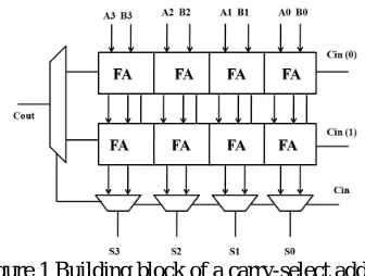
A.CARRY SELECT ADDER
Carry Select Adder is the fastest adders which are used in many data-processing processors to perform fast arithmetic operation. CSLA is used in many computational systems to alleviate the problem of carry propagation delay by independent generation multiple carries and then select a carry to generate the sum. However, the CSLA is not an power efficient because it uses multiple pairs of Ripple Carry Adders (RCA) to generate partial sum and carry by considering carry input as Cin=0 and Cin=1, then the final summation and carry are selected by the multiplexers.
ISSN(Online): 2320-9801
ISSN (Print) : 2320-9798
I
nternational
J
ournal of
I
nnovative
R
esearch in
C
omputer
and
C
ommunication
E
ngineering
(An ISO 3297: 2007 Certified Organization)
Vol. 4, Issue 3, March 2016
Figure 1 Building block of a carry-select adder
B. BINARY TO EXCESS-1 CONVERTER (BEC)
BEC is used to add 1 to the input numbers. The Boolean logic for 3-bit BEC has developed using ~NOT, &AND and ^XOR gates. It is very easy to develop higher bit size BEC architecture also because it has the same basic building block of AND and XOR gates for higher bits. To use BEC instead of the RCA with Cin=1 in order to reduce the power and power consumption of the regular CSLA. To replace the n-bit RCA, an n+1-bit BEC is required. The importance of the BEC logic stems from the large silicon power reduction when the CSLA with large number of bits are designed.
Figure 2 3 Bit Binary to Excess-1 Converter
Figure 2, shows the circuit of 3 bit Binary to Excess-1 Converter which has input as B0, B1 and B2, then produces
an output as X0, X1 and X2.
The Boolean expression of the 3 bit BEC are shown below:
X0 = ~B0 (1)
X1 = B0⊕ B1 (2)
X2 = B2⊕ (B1 × B0) (3)
In Table 1.1. the value of 001 is added to each 3-bit input number B and produces the 3-bit ouput number X.
BINARY [3:0] EXCESS-1 [3:0]
B2 B1 B0 X2 X1 X0
0 0 0 0 0 1
0 0 1 0 1 0
0 1 0 0 1 1
0 1 1 1 0 0
1 0 0 1 0 1
1 0 1 1 1 0
1 1 0 1 1 1
1 1 1 0 0 0
ISSN(Online): 2320-9801
ISSN (Print) : 2320-9798
I
nternational
J
ournal of
I
nnovative
R
esearch in
C
omputer
and
C
ommunication
E
ngineering
(An ISO 3297: 2007 Certified Organization)
Vol. 4, Issue 3, March 2016
C.CARRY LOOK-AHEAD ADDER (CLA)
A Carry Look-ahead Adder (CLA) is a type of adder used in digital logic. A CLA improves speed by reducing the amount of time required to determine carry bits. It can be contrasted with the simpler, but usually slower, ripple carry adder for which the carry bit is calculated alongside the sum bit. The CLA calculates one or more carry bits before the sum, which reduces the wait time to calculate the result of the larger value bits.
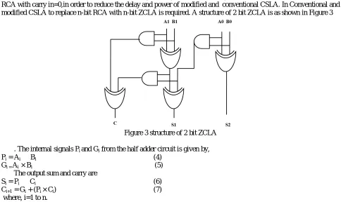
D.ZCLA
The main idea of this work to reduce the gate delay to use Zero Carry Look Ahead adder (ZCLA) instead of RCA with carry in=0,in order to reduce the delay and power of modified and conventional CSLA. In Conventional and modified CSLA to replace n-bit RCA with n-bit ZCLA is required. A structure of 2 bit ZCLA is as shown in Figure 3
Figure 3 structure of 2 bit ZCLA
. The internal signals Pi and Gi from the half adder circuit is given by,
Pi = Ai ⊕ Bi (4)
Gi = Ai × Bi (5)
The output sum and carry are
Si = Pi⊕ Ci (6)
Ci+1 = Gi + (Pi × Ci) (7)
where, i=1 to n.
Here, Gi is the carry generate signal and Pi is the carry propagate signal. In the case of ZCLA, C0=0.
II. RELATED WORK
A. CONVENTIONAL CSLA USING RCA
Conventional carry select adders generally consist of two ripple carry adders and multiplexers. Adding two n-bit numbers with a carry select adder is done with two adders(therefore two ripple carry adders) in order to perform the calculation twice, one time with assumptions of Cin=0 and other assuming Cin=1. After two results are calculated, the correct sum as well as the correct carry out is selected with multiplexer once the carry input is known. One input to the MUX goes from the RCA with Cin=0 and other input from the RCA with Cin=1. The upper adder has a carry-in of zero, the lower adder a carry-in of one. If the carry-in is zero, the sum and carry- out of the upper adder are selected. If the carry-in is one, the sum and carry-out of the lower adder are selected. The main disadvantage of regular CSLA is the large power due to the multiple pairs of ripple carry adder.
ISSN(Online): 2320-9801
ISSN (Print) : 2320-9798
I
nternational
J
ournal of
I
nnovative
R
esearch in
C
omputer
and
C
ommunication
E
ngineering
(An ISO 3297: 2007 Certified Organization)
Vol. 4, Issue 3, March 2016
B.16 BIT LINEAR and SQRT Conventional CSLA USING RCA
In Figure 4, 16-bit Linear Conventional Carry Select Adder has block size as 4 can be created with three of pair of RCA blocks and a 4 bit ripple carry adder. Since Cin is known at the beginning of computation, a carry select block
is not needed for the first four bits. Total delay of linear carry select adder will be four full adder delays, plus three MUX delays. The disadvantages of linear carry select adders are high power usage and high delay.
Figure 4 16-bit Linear Conventional CSLA Using RCA
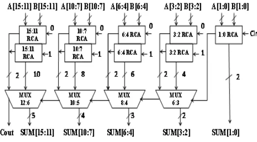
A square-root (SQRT) CSLA has to implement large bit-width adders with less delay. In a SQRT CSLA, CSLAs with increasing size are connected in a cascading structure. The main objective of SQRT-CSLA design is to provide a parallel path for carry propagation that helps to reduce the overall adder delay. The disadvantages of linear carry select adder can be rectified by SQRT CSLA. The time delay of the linear adder can decrease by having one more input into each set of adders than in the previous set.
‘
Figure 5 16-bit SQRT Conventional CSLA Using RCA
In figure 5, 16-bit SQRT Conventional Carry Select Adder having different block sizes can be created with 2, 3, 4, 5 bit pair of RCA and 2 bit ripple carry adder. The total delay is two full adder delays, and four MUX delays.
C. MODIFIED CSLA USING BEC-1
Instead of using a pair of RCA block, BEC based CSLA architecture has developed using a single ripple carry adder with Binary to Excess-1 converter, which replace the RCA block for Cin=1, in order to reduce the power and
ISSN(Online): 2320-9801
ISSN (Print) : 2320-9798
I
nternational
J
ournal of
I
nnovative
R
esearch in
C
omputer
and
C
ommunication
E
ngineering
(An ISO 3297: 2007 Certified Organization)
Vol. 4, Issue 3, March 2016
two possible partial results in parallel and the mux is used to select either the BEC output or the direct inputs according to the control signal Cin.
The RCA calculates n-bit sum and carry out corresponding to Cin=0. The BEC unit receives that sum and carry
out from the RCA and generates (n + 1)-bit excess-1 code. It is clear that BEC structure reduces the power but the disadvantage is that delay is high than conventional CSLA. The advantage of this BEC logic uses lesser number of logic gates.
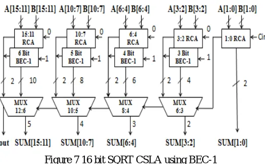
D.16 BIT LINEAR AND SQRT MODIFIED CSLA USING BEC-1
A 16 bit linear Modified CSLA using BEC-1 has a block size of 4 which can be created by LSB bit as a 4 bit RCA and the remaining bits can be created by the upper adder as 4 bit RCA and the lower adder as 5 bit BEC-1.
Figure 6 16 bit linear Modified CSLA using BEC-1
Figure 7 16 bit SQRT CSLA using BEC-1
A 16 bit SQRT Modified CSLA using BEC-1 having different block sizes can be created by LSB as a 2 bit RCA and the remaining bits are created by upper adder as 2, 3, 4 and 5 bits RCA and the lower adder as 3, 4, 5, 6 bits BEC-1.
III.PROPOSED WORK
A. PROPOSED CSLA USING ZCLA
ISSN(Online): 2320-9801
ISSN (Print) : 2320-9798
I
nternational
J
ournal of
I
nnovative
R
esearch in
C
omputer
and
C
ommunication
E
ngineering
(An ISO 3297: 2007 Certified Organization)
Vol. 4, Issue 3, March 2016
propagation with Cin=0 and the carry output is produced when the carry propagation is multiplied with Cin =0 then the result is OR’ed with carry generation. In the proposed CSLA, ZCLA is used instead of RCA with Cin=0 in conventional and modified CSLA. In this CSLA, sum is produced by carry propagation and the carry out is produced by carry generation results. MUX is used to select one input from upper adder and the other input from lower adder from which the correct sum and carry outputs are generated. Thus the power is much reduced when compared to conventional CSLA using RCA and modified CSLA using BEC-1.
B.16 BIT LINEAR AND SQRT Conventional CSLA USING ZCLA
The 16-bit Linear Conventional CSLA using ZCLA has a block size as 4 can be created by LSB has 4-bit ZCLA and the remaining CSLA blocks can be created by having upper adder with 4-bit ZCLA and the lower adder with 4-bit RCA with Cin=1.
Figure 8 16 bit Linear Conventional CSLA using ZCLA
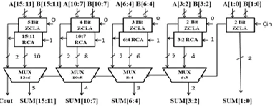
The 16-bit SQRT Conventional CSLA using ZCLA having different block sizes can be created by LSB has 2-bit ZCLA and the remaining CSLA blocks can be created by upper adder as 2, 3, 4 and 5 2-bits ZCLA and the lower adder as 2,3,4 and 5 bits RCA with Cin = 1.
Figure 9 16 bit SQRT Conventional CSLA using ZCLA
C. 16 BIT LINEAR AND SQRT Modified CSLA USING ZCLA
ISSN(Online): 2320-9801
ISSN (Print) : 2320-9798
I
nternational
J
ournal of
I
nnovative
R
esearch in
C
omputer
and
C
ommunication
E
ngineering
(An ISO 3297: 2007 Certified Organization)
Vol. 4, Issue 3, March 2016
Figure 10 16 bit Linear Modified CSLA using ZCLA
The 16-bit SQRT Modified CSLA using ZCLA having different block sizes can be created by LSB has 2-bit ZCLA and the remaining CSLA blocks can be created by upper adder as 2, 3, 4 and 5 bits ZCLA and the lower adder as 2,3,4 and 5 bits BEC-1.
Figure 11 16 bit SQRT Modified CSLA using ZCLA
IV.SIMULATION RESULTS
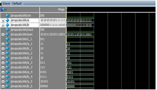
The 16 bit Linear and SRQT Carry Select Adders are analysed by Conventional, Modified and Proposed methods. The simulation of 16-bit CSLA is done by using MODELSIM and the power results are analyzed by using CADENCE.
The simulation result of 16-bit CSLA is shown in figure 12.
ISSN(Online): 2320-9801
ISSN (Print) : 2320-9798
I
nternational
J
ournal of
I
nnovative
R
esearch in
C
omputer
and
C
ommunication
E
ngineering
(An ISO 3297: 2007 Certified Organization)
Vol. 4, Issue 3, March 2016
POWER (nW)
METHODS LINEAR CSLA SQRT CSLA Conventional 275907.213 234160.071
Modified 25574.586 208511.826 PROPOSED
Conventional 22142.002 184973.812 Modified 19034.765 152821.318
Table 2 Power Analysis
V. CONCLUSION
The results prove that the Proposed CSLA using ZCLA have less power when compared with Conventional and Modified CSLA. Thus, the 16-bit SQRT CSLA is better than the 16-bit Linear CSLA. In future, we can analyze the 32 and 64 – bits in Linear and SQRT CSLA.
REFERENCES
1. Yogita and Hiremath, “A Novel 8-bit Carry Select Adder using 180nm CMOS Process Technology”, International Journal of Emerging Engineering Research and Technology, Volume 2, Issue 6, September 2014.
2. Mary Joseph and Renji Narayanan, “16 Bit Carry Select Adder with Low Power and Power” , International Journal on Recent and Innovation Trends in Computing and Communication , Volume: 2, Issue: 5.
3. Shrishti khurana and Dinesh Kumar Verma, “SQRT CSLA with Less Delay and Reduced Power Using FPGA”, International Journal of Research in Advent Technology, Vol.2, No.6, June 2014.
4. B. Ramkumar and H. M. Kittur, “Low-power and area-efficient carry-select adder,” IEEE Trans. Very Large Scale Integr. (VLSI) Syst., vol. 20, no. 2, pp. 371–375, Feb. 2012.
5. I.-C. Wey, C.-C. Ho, Y.-S. Lin, and C. C. Peng, “An power-efficient carry select adder design by sharing the common Boolean logic term,” in Proc. IMECS, 2012, pp. 1–4.
6. P. Thakare1 and S. Agrawal, “Design of High Efficiency Carry Select Adder Using SQRT Technique”, International Journal of Emerging Technology and Advanced Engineering, Volume 3, Issue 7, July 2013.
7. M. Vidhya and R. Muthammal,”A Novel Designing Approach for Low Power Carry Select Adder”, International Journal of Recent Trends in Electrical & Electronics Engg., April. 2014.
8. T.Y.Ceiang and M.J.Hsiao., (Oct. 1998). “Carry select adder using ripple carry adder”. Electron. Lett. , 2101-2103.
BIOGRAPHY
K.Anitha is a PG student of VLSI Design in Electronics Department, Dr. Sivanthi Aditanar College of Engineering College under Anna University, Chennai. She received her Bachelor of Engineering degree in 2014 from Dr. Sivanthi Aditanar College of Engineering.
E.Mangala MariSelvi is a PG student of VLSI Design in Electronics Department, Dr. Sivanthi Aditanar College of Engineering College under Anna University, Chennai. She received her Bachelor of Engineering degree in 2014 from Dr. Sivanthi Aditanar College of Engineering.
K.Vijayalakshmi is a PG student of VLSI Design in Electronics Department, Dr. Sivanthi Aditanar College of Engineering College under Anna University, Chennai. She received her Bachelor of Engineering degree in 2014 from Dr. Sivanthi Aditanar College of Engineering.