PARAKH, SAMYAK. High Bandwidth Supply Modulator Design for Envelope Tracking Application using 0.15um GaN on SiC (under direction of Dr. David Ricketts.)
200Watts DC-DC buck converter is designed with rise time of 9ns and efficiency of 86% against target of 10ns and 90% efficiency in AWR microwave office software.
Envelope Tracking (ET) is an increasingly popular technique used for maintaining good
efficiency in the RFPA (Radio Frequency Power Amplifier) across different output power levels. Efficiency of an RF amplifier can be improved by extracting the envelope of the RF signal and using that information to vary the supply of the RF amplifier.
Importance of GaN technology in power electronics along with its fundamental principles has also been described briefly. Also specifications of 0.15um GaN on SiC has been discussed. The technology used for this project is 0.15um GaN on SiC by Qorvo because of its high voltage, low On-resistance and small gate charge specifications.
This work mainly focusses on Design of multi-phase Buck switching converters, operating at very high switching frequency. Single phase and multi-phase converter principles have been understood and explained. Quasi Square Wave-Zero Voltage Switching [QSW-ZVS] have also been explored for achieving higher efficiency, better current sharing at high switching
frequencies.
Issues related to achieving ZVS, trade-offs behind using complex filters for achieving higher bandwidth, their advantages and the design methodology used has been explained.
© Copyright 2018 by Samyak Parakh
by Samyak Parakh
A thesis submitted to the Graduate Faculty of North Carolina State University
in partial fulfillment of the requirements for the degree of
Master of Science
Electrical Engineering
Raleigh, North Carolina
2018
APPROVED BY:
_______________________________ _______________________________ Dr. Brian Floyd Dr. John Muth
_______________________________ Dr. David Ricketts
DEDICATION
BIOGRAPHY
Samyak Parakh is currently pursuing his Master of Science in Electrical Engineering at North Carolina State University, Raleigh. His Master’s thesis under the guidance of Dr. Ricketts, deals with an Integrated Supply Modulator Design for Envelope Tracking Application using 0.15um GaN on SiC. He has been involved in many projects related to On-chip and system level power management and its application. He received his Bachelor of Engineering in Electronics and Instrumentation from Birla Institute of Technology and Science, Pilani K.K Birla Goa Campus in India. He was previously involved in Robotics, Physics and automation.
Samyak is a Research Assistant with Power America under the guidance of Dr. Ricketts. He did an internship with Dialog Semiconductors, California, where he worked on very high efficiency at very light loads DC-DC converters for mobile applications.
ACKNOWLEDGMENTS
First and foremost I would like to thank North Carolina State University for giving me this amazing opportunity to pursue higher studies Electrical Engineering. I am highly indebted to a lot of people I interacted during my journey at NCSU.
I am whole-heartedly indebted to my visionary Advisor, Dr. David Ricketts, Professor, NCSU for his astute and invaluable guidance, weekly discussions, thorough evaluation and prudent suggestions. I owe him gratitude for motivating me to undertake research thesis and providing unending academic and research inputs.
I am sincerely grateful to my MS research thesis evaluation jury- Dr. David Ricketts, Dr. John Muth and Dr. Bryan Floyd for having accepted to evaluate and examine my thesis work and for sparing their precious time.
I express my sincere gratitude to the authorities of NCSU, Power America and Lockheed Martin for providing me financial assistance as Research Assistant. My special thanks go to Dr. Yuanzhe Zhang, Dr. Dragan Maksimovic’, for their work is the foundation I have tried to build on.
I am also thankful to Akshat Shenoy and Shubhankar Patwardhan for their valuable inputs and suggestions.
TABLE OF CONTENTS
LIST OF TABLES ... vii
LIST OF FIGURES ... viii
Chapter 1 Objective and Background ... 1
1.1 Motivation ... 2
1.2 Topologies for supply modulator or ET Amp ... 4
Chapter 2 Technology ... 9
2.1GAN device two dimensional Electron Gas [2DEG] ... 9
2.2 0.15 µm GaN on SiC by Qorvo ... 10
Chapter 3 Buck ConverteR and ZVS operation ... 11
3.1 PWM Operation ... 11
3.2 Quasi Square Wave-Zero voltage switching operation ... 13
3.3 Filter Design ... 15
3.4 Linearity correction and PWM generation ... 18
Chapter 4 Multi phase Buck CoNverter... 19
4.1 Fourth order filter design in multi-phase buck converter ... 20
4.2 Auto current balancing due to ZVS ... 23
4.3 Summary on bandwidth limitations and trade-offs ... 24
Chapter 5 Complete Design and optimization ... 27
5.1 Driver Circuit ... 27
5.3 Efficiency analysis for Phase selection ... 34
5.4 Power analysis of 25 watts single phase buck converter... 39
5.5 Layout and dominant limiting factors ... 41
5.6 Parasitic Validation ... 43
5.7 Multi-phase system ... 45
5.8 Thermal limits ... 49
5.9 Higher frequency operation ... 51
Chapter 6 Conclusions and recommendations ... 52
References ... 53
LIST OF TABLES
Table1.1 Referenced design and their specifications ... 10
Table 2.1 0.15um GaN on SiC Process Parameters ... 19
Table 5.1 Different voltages in the circuit ... 36
Table 5.2 Filer component values single phase design 5 phase system ... 43
Table 5.3 Filer component values single phase design 6 phase system ... 44
Table 5.4 Filer component values single phase design 7 phase system ... 45
Table 5.5 Filer component values single phase design 8 phase system ... 46
Table 5.6 Final circuit and device sizes ... 47
LIST OF FIGURES
Figure 1.1 Typical PDF of high PAPR signal and PA efficiency for fixed supply voltage ... 11
Figure 1.2 Efficiency vs Pout in a RF Amp for fixed and optimum supply voltages ... 12
Figure 1.3 Top level block diagram for fixed and envelope tracking supply ... 12
Figure 1.4 Linear Regulator ... 12
Figure 1.5 General structure of switching converter ... 14
Figure 1.6 Duty Cycle ... 14
Figure 1.7 Circuit for Buck Converter ... 15
Figure 1.8 Circuit for Boost Converter ... 15
Figure 1.9 Circuit for Buck-Boost Converter ... 16
Figure 1.10 Serial hybrid topology of Supply modulator ... 17
Figure 1.11 Parallel hybrid topology of Supply modulator ... 17
Figure 2.1 2DEG formation in GaN/AlGaN interface and material properties ... 18
Figure 3.1 Typical buck converter circuit ... 20
Figure 3.2 PWM operation ... 21
Figure 3.3 Hard switching waveform QHS turn-on... 22
Figure 3.4 ZVS (soft) Switching waveform QHS turn-on ... 22
Figure 3.5 showing QSW-ZVS Operation ... 23
Figure 3.6 Buck converter ... 24
Figure 3.7 4rth Oder filter ... 25
Figure 4.1 Two phase buck converter and its waveforms ... 27
Figure 4.2 Thevenin Equivalent circuits for 2-phase buck converter with interleaved ... 29
Figure 4.3 Generalized thevenin equivalent circuit for N phase ... 30
Figure 4.4 Bode plot for TF(N) ... 31
Figure 4.5 Simplified model for filter designing ... 31
Figure 4.6 Current sharing auto balancing mechanism ... 32
Figure 4.7 Ripple reduction factor for two phase ... 33
Figure 4.8 Bode plot of an eight phase filter with and without TF (N) ... 34
Figure4.9 Achieving faster slew rate ... 35
Figure4.10 Output Voltage rise comparison in interleaved and faster slew operation ... 35
Figure 5.1 High side and low side driver with the power stage ... 36
Figure 5.2 Basic block used for driver design ... 36
Figure 5.3 Modified Active pullup driver ... 37
Figure 5.4 Circuit with power stage and their respective driver circuit... 38
Figure 5.5 High side Driver waveforms ... 38
Figure 5.6 Low side driver waveforms ... 39
Figure 5.7 Figure of buck converter ... 40
Figure 5.8 Rds (on) vs gate periphery ... 41
Figure 5.9 Circuit with Rds(on) of high side and low side during On and off time ... 41
Figure 5.10 Per-phase Efficiency vs Gate periphery (W) for 5 phase system ... 43
Figure 5.12 Per-phase Efficiency vs Gate periphery (W) for 7 phase system ... 45
Figure 5.13 Per-phase Efficiency vs Gate periphery (W) for 8 phase system ... 46
Figure 5.14 Buck converter power stage with driver ... 47
Figure 5.15 Efficiency plot for single phase ... 48
Figure 5.16 Loss distribution for 0.75 duty cycle ... 48
Figure 5.17 Loss distribution for 0.5 duty cycle ... 49
Figure 5.18 Loss distribution for 0.2 duty cycle ... 49
Figure 5.19 Complete Layout with different blocks ... 51
Figure 5.20 key parasitic elements associated with a switch ... 52
Figure 5.21 post and pre parasitic extracted waveforms ... 53
Figure 5.22 Bode plot of filter for 8-phase using only simplified model and with TF(N) ... 54
Figure 5.23 Output voltage and power for step change in duty cycle (0.2-0.75) ... 55
Figure 5.24 Phase currents during step change ... 55
Figure 5.25 Bode plot of filter for 8-phase with simplified model and also with TF(N) ... 56
Figure 5.26 Output voltage and power for step change in duty cycle (0.2-0.75) ... 57
Figure 5.27 Currents for 4 phases during step change ... 57
Figure 5.28 GaN device structure ... 58
Figure 5.29 Thermal simulations of 10 x 100um device ... 59
CHAPTER 1
OBJECTIVE AND BACKGROUND
The aim of this work was to make a simulation based power supply design for envelope tracking application. The target specifications for the design includes less than 10ns rise time (10%-90%) in output voltage, Peak output power of 200 watts and peak efficiency close to 90%. Simultaneously understand the limits and limiting factor for total output power and achievable bandwidth. Table1.1 shows reference designs for DC-DC converters for similar applications.
Table 1.1 Referenced design and their specifications
Index Tech power Bandwidth Per-phase 𝐹𝑆 Peak efficiency Phases
1 silicon 50 Watts 10MHz 15 MHz 95% 8
3 0.7um GAN 1.9 Watts 20MHZ 200MHZ 64.1% 1
2 0.25um GaN 3.3 Watts 20MHZ 200MHZ 73% 1
4 0.15um GaN on SiC
7 watts 20MHZ 100MHZ 90% 1, 2
1.1 Motivation
Envelope Tracking (ET) is an increasingly popular technique used for maintaining good efficiency of the RF (Radio Frequency) power amplifier (PA) across different output power levels.
Wireless communication systems like Long Term Evolution (LTE) and Third Generation (3G), employ large bandwidth (BW) digital modulated signals which has very high Peak-to-Average Power Ratio (PAPR). Also due to wide used of complex modulation schemes like QAM (Quadrature Amplitude Modulation) which can enable higher data rates, requires both amplitude and phase modulations and this forces RF PAs to operate in linear region [5,6].
Within the realm of linear region for a given supply voltage RFPA has peak efficiency at a particular output power after which it starts to become nonlinear, though when operated in lower than peak output power (backed off mode) [7, 8], which happens majority of the time in modulated signal with high PAPR, the efficiency drops significantly. Which can be critical in wireless systems in battery operated devices like cellphone antenna and also in Cellphone base stations [9].
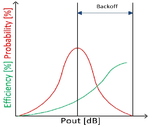
Typical high PAPR signal can have median output power much lower than its peak Output power, Fig 1.1 shows probability density function of a high PAPR RF signal and how average efficiency can become very low in case we have a fixed supply.
Figure 1.2 Efficiency vs Pout in a RF Amp for fixed and optimum supply voltages
Optimum supply curve shown in Figure 1.2 shows that by employing a different supply voltages at different output power level we can maintain higher efficiency in RF Amps [10].
Figure 1.3 Top level block diagram for fixed and envelope tracking supply for RF systems
Envelope tracking tries to do that dynamically using information of RF Amp’s input envelope.
1.2 Topologies for supply modulator or ET Amp
Performing the function of supply modulation for RF may require very high bandwidth, below mentioned are list of possible topologies:
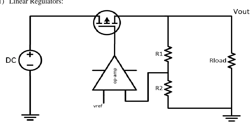
1) Linear Regulators:
Figure 1.4 Linear Regulator
Linear regulators in Figure 1.5 are like a variable resistors in series with the supply voltage, making use of negative feedback network it is able to change the pass transistor’s drive which in turn help change its resistance.
𝜂 (𝑒𝑓𝑓𝑖𝑐𝑖𝑒𝑛𝑐𝑦) = 𝑉𝑜𝑢𝑡 × 𝐼𝑙𝑜𝑎𝑑
𝑉𝑖𝑛 × (𝐼𝑙𝑜𝑎𝑑 + 𝐼𝑞𝑢𝑒𝑠𝑖𝑒𝑛𝑡)
Ideal case If Iq~0
𝜂 = 𝑉𝑜𝑢𝑡/𝑉𝑖𝑛
2) Switching converters:
Figure 1.5 General structure of switching converter
DC-DC Switching converters are becoming omnipresent in today’s electronics. They are extremely useful and capable of providing high Efficiency, in case of varying input voltage supply (eg. batteries) and multiple levels of output voltage requirement like laptop power systems [12]. DC-DC converter consists of Input DC supply, network of switches, Inductors and Capacitors and a controller. The network is used for stepping-up, stepping-down or both, the input voltage. These reactive-passive networks transform and filter the potential level and creates a low impedance supply voltage but does contains a small high frequency switching ripple. An ideal switching converter has 100% efficiency.
There are many control strategies possible, the most commonly used is called Pulse Width Modulation (PWM). It uses D (Duty Cycle) as a means to control output voltages. Where D is defined as percentage of time a particular switch is on (𝑡𝑜𝑛) fixed switching period (𝑇𝑠).
𝐷 =𝑡𝑜𝑛 𝑇𝑠
Figure 1.6 Duty Cycle
Controller
Input DC Supply
Network of Switches, Inductors and
Capacitors
Basic DC-DC converter Topologies:
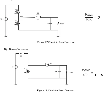
A) Buck Converter
The circuit below is a Buck Converter. This converter can provide any voltages between 0V to Vin and is the most commonly used topology used in industry. It also has one of the simplest closed loop controls.
𝑉𝑜𝑢𝑡
𝑉𝑖𝑛
= 𝐷
Figure 1.7 Circuit for Buck Converter
B) Boost Converter
𝑉𝑜𝑢𝑡
𝑉𝑖𝑛
=
1
1 − 𝐷
Figure 1.8 Circuit for Boost Converter
This converter can theoretically provide any voltages at the output between ∞ to Vdc. This converter has a right hand plane zero in its small signal transfer function which can be a
C) Buck-Boost Converter
𝑉𝑜𝑢𝑡
𝑉𝑖𝑛
=
−𝐷
1 − 𝐷
Figure 1.9 Circuit for Buck-Boost Converter
This converter can theoretically provide any voltages at the output between 0 to -∞. This converter also has a right hand plane zero in its small signal transfer function which can be a limitation in achieving higher bandwidth [13, 14].
Since, we are looking for a supply which can support variable output voltage with high efficiency, dynamic supply must use a DC-DC converter because that can perform efficient voltage conversion across Vout.
DC-DC converter does have lower bandwidth and higher output ripple compared to linear regulators. But with the development of wide band gap GaN based transistors it’s possible to achieve very high bandwidth switching converters due to their better figure of merits [15].
3) Hybrid topologies:
Hybrid topology tries to take advantage of best of both the worlds, higher bandwidth of linear regulators and higher efficiency of switching converters. Switching regulator can provide low frequency portion of the envelope with higher efficiency and linear regulators can provide high frequency part with low efficiency [16]. We can connect Linear and Switch mode supplies either in serial or parallel combination.
A) Serial hybrid
signal and switching converter is tracking the envelope of the RF signal’s envelope. This is achieved by providing variation in linear regulator’s supply and tries to always keep voltage
difference between its input and output small [17].
Figure 1.10 Serial hybrid topology of Supply modulator
B) Parallel hybrid
Parallel topology is one more hybrid way of supply modulation. In this case as shown in Figure 1.12 the Currents from switching converter and linear regulator are added and given to a RF amplifier. This circuit is operated in closed loop current controlled fashion. The bulk of the power is provided by high efficiency switching converter and higher frequency content is provided by high bandwidth linear regulator [17].
CHAPTER 2
TECHNOLOGY
We used GaN technology as it has various advantages over silicon especially in very high frequency applications. Few fundamental phenomena operating in GaN devices are discussed next.
2.1 GAN device two dimensional Electron Gas [2DEG]
The piezoelectric property of GaN comes from its Wurtzite lattice structure, mainly present because of small shift in atoms in lattice with introduction of external strain. When a thin layer of AlGaN (Aluminum Gallium Nitride) is grown on top of GaN, due to difference in their lattices, a strain is introduced which intern produces a 2DEG as shown in the figure 2.1 below [18]. The presence of electrons in very thin layer without any presence of dopants is the fundamental principle behind High Electron Mobility Transistor [HEMT’s].
Figure 2.1 2DEG formation in GaN/AlGaN interface and material properties of GaN and Si
GaN devices have many disadvantages like, trapping effects can reduce the device performance and hot electron presence can degrade the device performance and cause reliability issues [19].
Silicon Carbide as a substrate provides good thermal conductivity which is generally very helpful in high power circuits.
Properties GaN Si
Band Gap (eV) 3.39 1.12
Critical Field (V/m) 3.3 0.23
Electron Mobility (cm2/V-s) 1500 1400
2.2 0.15 µm GaN on SiC by Qorvo
The Qg is the gate charge, it is the total charge required for switching on the device from an Off-State. Gate charge is directly proportional to the size of the device and is a metric for switching loss due to the device operation.
Ron is the On-Resistance that a device offers when fully on it is inversely proportional to device size. Ron is a metric for conduction loss due to the device. Combining both the factors gives us:
𝐹𝑂𝑀 = 𝑄𝑔 × 𝑅𝑂𝑁
The smaller the value implies higher the efficiency for a given switching frequency and a given load. In case of 0.15 µm GaN on SiC from Qorvo they have one of the best FOM 19pV-s along with SiC substrate which also provides good thermal conduction as SiC has excellent thermal conduction coefficient.
Only n type Depletion mode devices are available in the design kit, some of the key parameters associated are listed below.
Table 2.1 0.15um GaN on SiC Process Parameters
The breakdown is 50 V, they don’t have body diodes but can do reverse conduction when the drain terminal drops Vth below the gate [15]. These GaN device can be used as a schottky diode using gate as anode and drain and/or source as cathode.
Parameter Value
Recommended DC bias (VDS) 28V Threshold Voltage (Vth) -3.5V
CHAPTER 3
BUCK CONVERTER AND ZVS OPERATION
3.1 PWM Operation
Figure 3.1 Typical buck converter circuit
During the on time [QHS on] the inductor current rises with a slope of 𝑉𝐷𝐶−𝑉𝑜𝑢𝑡
𝐿 and during off time [QHS off] falls with a slope of−𝑉𝑜𝑢𝑡
𝐿 . In the figure. 3.1, it shows the duty cycle, on time and off time with corresponding inductor current and switch node voltage waveform.
Between QHS turning off and QLS turning on there is a small time when both QHS and QLS is off, this time is called dead time. Dead time has very important role to play as it ensures that there is no moment when both QHS and QLS is switched on, since if that were to happen it would create short circuit between Vin and Ground. Then the switching node voltage is filtered out using LC filter and given it to the load R. The filter can be designed in such a way that all the ripple at the SW node is attenuated very well and what we see at the output will be the average value of voltage at the switching node (with small ripple).
The average value at the output can then be calculated using small ripple approximation as: 𝑉𝑜𝑢𝑡 = 𝐷 × 𝑉𝑖𝑛
Inductor current flows through the QLS body diode during the dead time, which ensures that when QLS starts to switch on it only has forward voltage drop of the body diode (VF) which is very small compared to Vin. This phenomena Zero Voltage Switching (ZVS) helps in reducing switching loss in high to low transition and in case of buck converter we have a natural high to low switch node transition a ZVS transition.
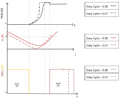
3.2 Quasi Square Wave-Zero voltage switching operation
The low to high transition in PWM mode can cause significant power loss and is called hard switching. Simultaneous or overlapping presence of voltage and current across switches due to their finite speed as shown in fig 3.3.
Figure 3.3 Hard switching waveform QHS turn-on
𝑃𝐻𝐴𝑅𝐷 =1
2× 𝑇𝑆𝑊× 𝑉𝑑𝑠 × 𝐼𝐷× 𝐹𝑆
To get rid of this hard switching loss we can design the buck converter’s inductor in fig444 in such a way that he current ripple is large enough such we have the minimum current less than zero, across loads. If the current is negative when QLS turns off, this negative current starts discharging Vsw node and then can start conducting through QHS’ body diode. This process
makes sure that when the QHS starts turning on, VDS across it is very low (~VF), this makes the low to high transition also becomes ZVS [20].
Shown below is the waveform after implementing the ZVS, which clearly shows the switch node voltage variation which causes the reduced turn on losses now in both the devices.
Figure 3.5 Showing QSW-ZVS Operation
Advantages:
a) Makes the low to high transition ZVS, improves efficiency
3.3 Filter Design
1) Second order ZVS filter design:
Figure 3.6 Buck converter
𝐼𝐿𝑂𝐴𝐷_𝑀𝐴𝑋 = 𝐷𝑀𝐴𝑋× 𝑉𝐼𝑁 𝑅𝐿𝑜𝑎𝑑
For maintaining ZVS through all the loads, the current ripple should be at least two times the max load.
2 × 𝐼𝐿𝑂𝐴𝐷_𝑀𝐴𝑋 ≤𝑉𝑖𝑛 × (1 − 𝐷𝑀𝐴𝑋)
𝐿 ×
𝐷𝑀𝐴𝑋 𝐹𝑠
𝐿 ≤ 𝑉𝑖𝑛 × (1 − 𝐷𝑀𝐴𝑋) 2 × 𝐼𝐿𝑂𝐴𝐷𝑀𝐴𝑋 ×
𝐷𝑀𝐴𝑋 𝐹𝑆 =
𝑅𝐿× (1 − 𝐷𝑀𝐴𝑋) 2 × 𝐹𝑆
Capacitor is decided by the voltage ripple requirement and/or bandwidth requirement. By selecting C we choose the resonant frequency of the filter, quality Factor and attenuation at switching frequency all at the same time.
𝑄 = 𝑅 × √𝐶
If we choose the inductor using equality
𝐿 =𝑅𝐿× (1 − 𝐷𝑀𝐴𝑋) 2 × 𝐹𝑆
Output voltage ripple at 𝐼𝐿𝑂𝐴𝐷_𝑀𝐴𝑋:
𝑉𝑅𝐼𝑃𝑃𝐿𝐸 =1 2×
𝑇𝑆 2 ×
𝐼𝐿𝑂𝐴𝐷 𝐶
𝐴𝑡𝑡𝑛~ 40𝑑𝐵 × 𝐿𝑜𝑔(𝐹𝑆𝑊 𝐹𝑅𝐸𝑆)
Equations above tells us that if we want to achieve 40-50 dB attenuation we will have keep the bandwidth < 1
10× 𝐹𝑆𝑊.
In order to have more flexibility in choosing higher bandwidth and still be able to have good ripple while achieving ZVS, it’s a good idea to use higher order filter.
2) Fourth Order ZVS filter design:
Figure 3.7 4rth Oder filter
Assuming both resonant double poles are separate and have minimal interaction:
𝐹𝑅𝐸𝑆1=
2 × 𝜋
√𝐿1𝐶1, 𝐹𝑅𝐸𝑆2=
L1 can still be designed from previous discussion of ZVS because we are assuming 𝐹𝑅𝐸𝑆1 & 𝐹𝑅𝐸𝑆2 are separate [20].
𝐿1 ≤𝑉𝑖𝑛 × (1 − 𝐷𝑀𝐴𝑋) 2 × 𝐼𝐿𝑂𝐴𝐷𝑀𝐴𝑋 ×
𝐷𝑀𝐴𝑋 𝐹𝑆 =
𝑅𝐿 × (1 − 𝐷𝑀𝐴𝑋) 2 × 𝐹𝑆
𝐿𝑒𝑡 𝐹𝐶 = 𝐹𝑅𝐸𝑆2= 2 × 𝜋 √𝐿2𝐶2
For flat response within the bandwidth:
𝑄2 = 𝑅𝐿 √(√𝐶2 𝐿2< 1
The attenuation can be approximately given by:
𝐴𝑡𝑡 (𝑑𝐵) = 40 log ( 𝐹𝑆
𝐹𝑅𝐸𝑆1) + 40 log ( 𝐹𝑆 𝐹𝑅𝐸𝑆2)
L1 is calculated from ZVS condition and we can choose 𝐴𝑡𝑡(𝑑𝐵) and Q2 value required and then rest of the component values can be found.
And we can justify our assumption of separate resonant frequencies by verifying:
3.4 Linearity correction and PWM generation
One of the main reason of not pursuing discontinues conduction mode, in DCM the output to input steady state transfer function becomes very non-linear.
Though some non-linearity still exists due to Rds(on) voltage drop and also due to zero voltage
switching [21]. This non linearity can be removed by making a lookup table of 𝜇 =𝑉𝑜𝑢𝑡 𝑉𝑖𝑛 vs 𝐷, this will ensure the right duty cycle for the output voltage we need.
Figure 3.8 Voltage conversion ratio vs duty cycle
1) FPGA
CHAPTER 4
MULTI PHASE BUCK CONVERTER
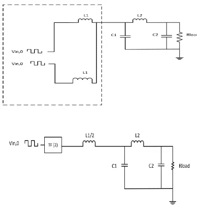
As we go towards higher power and higher bandwidth applications multi-phase converter start becoming the ideal choice especially if the efficiency is an important factor in design consideration.
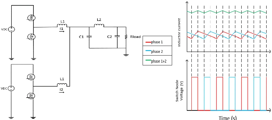
Generally a multi-phase buck converter is operated in an interleaving fashion where each phase leg has a phase difference of ∆𝜑 with the next leg as shown in fig 4.1.
∆𝜑 =(2 × 𝜋) 𝑁
𝑪
Because inductor current from each phase cancel each other this in effect reduces the output and input current ripple. This current ripple reduction also decreases voltage ripple and help increase the bandwidth as well reduce the size of passive components [22].
4.1 Fourth order filter design in multi-phase buck converter
Multi-phase converter can also have a 4rth order filter with ZVS, it helps in achieving high bandwidth and small overshoot in step changes.
For designing the filter the thevenin equivalent model of the interleaving multi-phase converter shown in Figure 4.2 has been used [17]. Here both phase has been replaced by a square wave with the second phase has a delay of 𝜋𝐶 (1800 𝑜𝑟𝑇𝑆
2).
The transfer function TF for N = 2 is given by:
𝑇𝐹(𝑁 = 2) =1
2× (1 + 𝑒
−𝑇2𝑆) : 𝑇
𝑆 = 𝑠𝑤𝑖𝑡𝑐ℎ𝑖𝑛𝑔 𝑡𝑖𝑚𝑒 𝑝𝑒𝑟𝑖𝑜𝑑
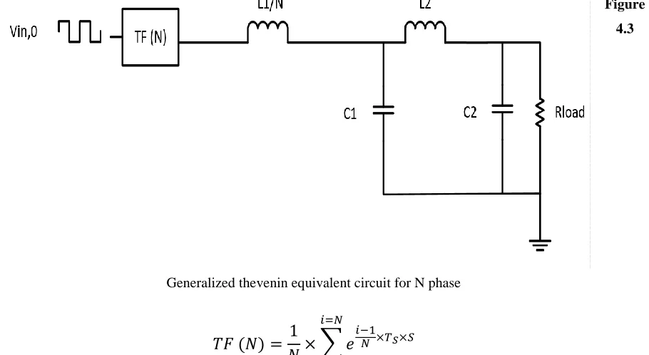
We can generalize this analysis for N phases:
Figure
4.3
Generalized thevenin equivalent circuit for N phase
𝑇𝐹 (𝑁) = 1
𝑁× ∑ 𝑒 𝑖−1
𝑁 ×𝑇𝑆×𝑆
𝑖=𝑁
𝑖=1
N = number of phases, 𝑇𝑆 = 1
𝐹𝑆 = 𝑠𝑤𝑖𝑡𝑐ℎ𝑖𝑛𝑔 𝑡𝑖𝑚𝑒 𝑝𝑒𝑟𝑖𝑜𝑑
TF(N) is a transfer function of sum of delays, which effectively generates a notch filters at the switching frequency (for N=2), such that we only need to filter out ripple at 𝑓 ≥ 2 × 𝐹𝑆.
Similarly for N phases we have to filter out ripple harmonics for:
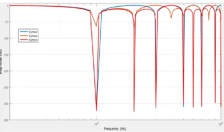
Figure 4.4 shows Bode plot for 𝑇𝐹 (𝑁 = 2,3,4) for 𝐹𝑆 = 100 𝑀𝐻𝑧:
Figure 4.4 Bode plot for 𝑇𝐹(N)
Thinking about the interleaving as a notch filter as previously described, the simplified model shown in Figure 3.5 can then be utilized along with 4rth Oder filter design methodology discussed previously in section 4.1. This now becomes a design where we have to remove the ripple at frequency at 𝑁 × 𝐹𝑆 instead of 𝐹𝑆.
4.2 Auto current balancing due to ZVS
Multi-phase converters in general has an issue of unequal current sharing between different phases. Doing QSW-ZVS [Quasi Square Wave] control in multi-phase buck converter has an inherent current balancing mechanism in place.
Figure 4.6 Current sharing auto balancing mechanism
4.3 Summary on bandwidth limitations and trade-offs
1) Single phase converter
Bandwidth is ultimately limited by the switching frequency and required attenuation. The type of filter used determines the rate of attenuation, like in case of second order LC filter which gives us approximately 40 db/decade of attenuation. So if we need an attenuation of about 40dB our bandwidth is limited to ~1/10th of Fsw. Here we can trade-off attenuation with bandwidth. Another way we can increase the bandwidth by increasing the order of our LC filter, it gives us more degree of freedom and also increases the rate of attenuation, since we now have faster attenuation due to presence of extra double pole. We can push the bandwidth to higher value and we still have similar trade-offs between attenuation and bandwidth.
2) Multi-phase buck converter
Multiphase converters are very good way of having more power but also increasing effective switching frequency = 𝑁 × 𝐹𝑆 when they are operated in an interleaving fashion. The ripple at frequency = 𝑁 × 𝐹𝑆 has a duty cycle dependent ripple reduction factor 𝐾 [24].
𝐾 = ∏ |𝑖 − 𝑁 × 𝐷| 𝑁
1
∏𝑁−11 (|𝑖 − 𝑁 × 𝐷| + 1) ∶ 𝐷 = 𝐷𝑢𝑡𝑦 𝐶𝑦𝑐𝑙𝑒, 𝑁 = 𝑛𝑢𝑚𝑏𝑒𝑟 𝑜𝑓 𝑝ℎ𝑎𝑠𝑒𝑠
Figure 4.7 Ripple reduction factor for two phase
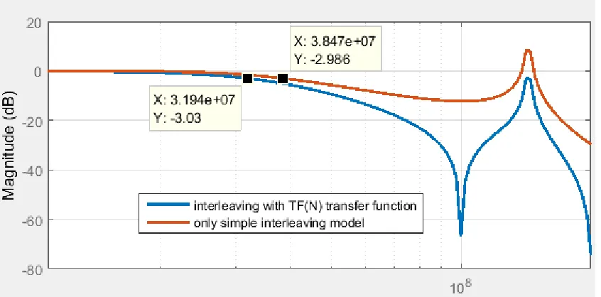
From the thevenin equivalent model in section 3.3 the switching ripple is shifted to frequency = 𝑁 × 𝐹𝑆 by introducing notch filters at harmonics of Fs till (𝑁 − 1) × 𝐹𝑆, but the ultimate bandwidth is still limited by switching frequency. But now we can move the bandwidth very close to switching filter without trading off on attenuation and even with second order filter. Though the bandwidth gets reduced by the effect of notch at switching frequency as we move the bandwidth higher. We can clearly see the reduction in bandwidth from 38.5 to 32 MHz.
Figure 4.8 Bode plot of an eight phase filter with and without TF (N)
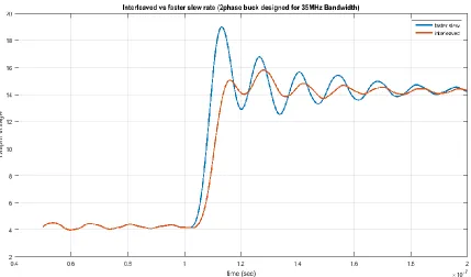
3) Faster slew rate
In multi-phase converters we can also achieve faster slew rate by leaving interleaving operation transiently and then going back again. We can trade off faster rise time at output with some overshoot at output voltage and phase currents.
Figure 4.9 Achieving faster slew rate
Figure 4.10 Output Voltage rise comparison in interleaved and faster slew operation
CHAPTER 5
COMPLETE DESIGN AND OPTIMIZATION
5.1 Driver Circuit
A 5W (7W peak) Buck converter was designed using 0.15um GaN on SiC in 4rth reference design [15], that work has been used as a foundation. The design includes an innovative driver design for the high side called modified active-pullup driver as shown in figure 5.1.
Figure 5.1 High side and low side driver with the power stage
Table 5.1 Different voltages in the circuit
Vin Vss,HS Vss,LS Vin,HS Vin,LS
20V -8V -5V -8/-13 V -5/-10V
In the sauration state in the GaN transistor current can be given by: 𝐼𝐷 ≈ 𝑘(𝑉𝐺𝑆− 𝑉𝑇𝐻)2
Fig 5.2 Basic block used for driver design
𝐼𝐷 ≈ 𝑘(𝐼𝐷× 𝑅1− 𝑉𝑇𝐻)2
𝐼𝐷 = 1 − 2 × 𝐾 × 𝑅1× 𝑉𝑇𝐻− √1 − 4𝐾 × 𝑅1× 𝑉𝑇𝐻 2 × 𝐾 × 𝑅12
We can see that by varying the resistor R1 in the circuit above we can make constant current sources, this strucure then has been used to drive QHS and QLS.
Figure 5.3 Modified Active pullup driver
Advantages of this driver is that it has less DC losses by virtue of making use of the switching node instead of the supply voltage (Vin), This can be done because the device QHS is fully on when VGS = 0 as it’s a depletion mode device.
1) Dynamic response and driver output connection:
Figure 5.4 Circuit with power stage and their respective driver circuit
Figure 5.5 High side Driver waveforms
Figure 5.6 Low side driver waveforms
In both the high side and low side driver the power device can be driven either from above or from below the resistor R1/R2. If we choose to drive from above R1/R2 then we are making QHS/QLS turn on transition faster and if from below R1/R2 then we are making QHS/QLS turn off transition faster.
In the circuit shown in Figure 2.4 QLS is being driven from bottom of R2 as it makes the turn off faster, because the turn on is already a ZVS this is the best choice for decreasing net losses.
5.2 Power Stage design
Figure 5.7 Figure of buck converter
Assuming no size limits no current limits:
Let’s assume 𝐷𝑀𝐴𝑋= 0.75
This gives us 10% margin for the dead time, 5% margin for rise and fall time of the switch node and also if we observe performance degradation due to increase in temperature we can get higher power by increasing duty cycle till 0.85.
This gives us 𝑉𝑂𝑈𝑇𝑀𝐴𝑋 = 𝐷𝑀𝐴𝑋× 𝑉𝐼𝑁= 0.75 × 20𝑉 = 15𝑉
𝑃𝑂𝑈𝑇𝑀𝐴𝑋 = 200 𝑊𝑎𝑡𝑡𝑠 ≤𝑉𝑂𝑈𝑇𝑀𝐴𝑋 2
𝑅𝐿𝑂𝐴𝐷 = 152 𝑅𝐿𝑂𝐴𝐷
𝑅𝐿𝑂𝐴𝐷 ≤ 225
200 = 1.125Ω
𝑅𝐿𝑂𝐴𝐷= 1Ω
1) Rds (on) Analysis:
The Rds (on) or on resistance of the device is calculated when fully on in Figure 5.8.
Figure 5.8 Rds (on) vs
gate
periphery
The Rds(on) per unit width of the device can be approximately calculated as 2Ω-mm.
Figure 5.9 Circuit with Rds (on) on high side and low side during On and off time
Now calculating minimum widths required for generating output power of 200 Watts for an N phase buck converter. High and low side widths have been made same for symmetry.
𝐼𝑙𝑎𝑣𝑔= 𝐼𝑙𝑜𝑎𝑑 =
𝑉𝑜𝑢𝑡𝑎𝑣𝑔 𝑅𝑙𝑜𝑎𝑑
𝑉𝑜𝑢𝑡𝑎𝑣𝑔= (𝐷 × 𝑉𝑖𝑛 −𝑉𝑜𝑢𝑡𝑎𝑣𝑔
𝑅𝑙𝑜𝑎𝑑 × 𝑅𝑑𝑠𝑜𝑛)
𝑉𝑜𝑢𝑡𝑎𝑣𝑔(1 +
𝑅𝑑𝑠𝑜𝑛
𝑅𝑙𝑜𝑎𝑑) = 𝐷 × 𝑉𝑖𝑛
𝑉𝑜𝑢𝑡𝑎𝑣𝑔 = 𝐷 ×
𝑉𝑖𝑛 1 +𝑅𝑑𝑠𝑜𝑛
𝑅𝑙𝑜𝑎𝑑
𝑃𝑜𝑢𝑡 ≥𝑉𝑜𝑢𝑡𝑎𝑣𝑔 2 𝑅𝑙𝑜𝑎𝑑 =
(𝐷 × 𝑉𝑖𝑛
1 +𝑅𝑑𝑠𝑜𝑛𝑅𝑙𝑜𝑎𝑑 )
2
𝑅𝑙𝑜𝑎𝑑 From previous discussion we can take:
𝑃𝑜𝑢𝑡 (𝑝𝑒𝑟 𝑝ℎ𝑎𝑠𝑒) =200
𝑁 𝑊, 𝑅𝑙𝑜𝑎𝑑 = 𝑁Ω, 𝑅𝑑𝑠𝑜𝑛 = 2 𝑊 𝑁 = 𝑛𝑢𝑚𝑏𝑒𝑟 𝑜𝑓 𝑝ℎ𝑎𝑠𝑒𝑠 200 𝑁 ≥ ( 15
1 +𝑁 × 𝑊2 )
2
𝑁
We can now calculate minimum width of high and low side device:
𝑊𝑀𝐼𝑁≈ 33 𝑁
5.3 Efficiency analysis for Phase selection
In this analysis the total system power, bandwidth and switching frequency is kept constant at 200 watts, 20 MHz and 100 MHz respectively. Number of phases have been varied and efficiency variation with device sizes has been observed in per-phase design.
A) Design for 5 phase buck converter system:
Single phase buck converter design with Pout = 40 watts
𝑅𝑙𝑜𝑎𝑑
𝑝ℎ𝑎𝑠𝑒= 𝑁 𝑜ℎ𝑚𝑠 = 5 𝑜ℎ𝑚𝑠, 𝐴𝑡𝑡𝑒𝑛𝑢𝑎𝑡𝑖𝑜𝑛 = ~45𝑑𝐵
Using the filter design procedure mentioned in section 4.1, we get following values for passive components.
Table 5.2 Filer component values single phase design 5 phase system
Parameter L1 C1 L2 C2 Rload BW
Value 6.25nH 3.075nF 49.7nH 1.273pF 5Ω 20 MHz
Figure 5.10 Per-phase Efficiency vs Gate periphery (W) for 5 phase system
B) Design for 6 phase buck converter system
Single phase buck converter design with Pout ≥ ~ 33 watts
𝑅𝑙𝑜𝑎𝑑
𝑝ℎ𝑎𝑠𝑒= 𝑁 𝑜ℎ𝑚𝑠 = 6 𝑜ℎ𝑚𝑠, 𝐴𝑡𝑡𝑒𝑛𝑢𝑎𝑡𝑖𝑜𝑛 = ~45𝑑𝐵
Using the filter design procedure mentioned in section 4.1, we get following values for passive components.
Table 5.3 Filer component values single phase design 6 phase system
Parameter L1 C1 L2 C2 Rload BW
Value 7.5nH 2.56nF 59.6nH 1.06pF 6Ω 20 MHz
Figure 5.11 Per-phase Efficiency vs Gate periphery (W) for 6 phase system
C) Design for 7 phase buck converter system
Single phase buck converter design with Pout ≥ ~ 28 watts
𝑅𝑙𝑜𝑎𝑑
𝑝ℎ𝑎𝑠𝑒= 𝑁 𝑜ℎ𝑚𝑠 = 7 𝑜ℎ𝑚𝑠, 𝐴𝑡𝑡𝑒𝑛𝑢𝑎𝑡𝑖𝑜𝑛 = ~45𝑑𝐵
Using the filter design procedure mentioned in section 4.1, we get following values for passive components.
Table 5.4 Filer component values single phase design 7 phase system
Parameter L1 C1 L2 C2 Rload BW
Value 8.75nH 2.197nF 69.6nH 0.90pF 7Ω 20 MHz
Figure 5.12 Per-phase Efficiency vs Gate periphery (W) for 7 phase system
D) Design for 8 phase buck converter system
Single phase buck converter design with Pout ≥ ~ 25 watts
𝑅𝑙𝑜𝑎𝑑
𝑝ℎ𝑎𝑠𝑒= 𝑁 𝑜ℎ𝑚𝑠 = 8 𝑜ℎ𝑚𝑠, 𝐴𝑡𝑡𝑒𝑛𝑢𝑎𝑡𝑖𝑜𝑛 = ~45𝑑𝐵
Using the filter design procedure mentioned in section 4.1, we get following values for passive components.
Table 5.5 Filter component values single phase design 8 phase system
Parameter L1 C1 L2 C2 Rload BW
Value 10nH 1.92nF 79.57nH 795pF 8Ω 20 MHz
Figure 5.13 Per-phase Efficiency vs Gate periphery (W) for 8 phase system
E) Final Circuit
Figure 5.14 Buck converter power stage with driver
Table 5.6 Final circuit and device sizes
Q1 Q11 R1 Q2 Q22 R2
4x75um 4x75um 40Ω 4x75um 8x75um 10Ω
QHS DHS QLS DLS
5x1.5mm 10x10x12um 7.5mm 16x10x12um
High side device, 2.88, 9.87%
Low side device, 0.5, 1.71%
High side diode, 0.01, 0.03% low side diode,
0.18, 0.62%
High side driver, 0.27, 0.93%
Low side driver, 0.57, 1.95% Pout, 24.77,
84.89%
Losses, 4.41 15.11%
Loss Disribution for D = 0.75
High side device Low side device High side diode low side diode High side driver Low side driver Pout
5.4 Power analysis of 25 watts single phase buck converter
Figure 5.15 Efficiency plot for single phase
Loss distribution for different duty cycles:
High side device, 2.54, 15.12%
Low side device, 0.72, 4.29%
High side diode, 0.15, 0.89%
low side diode, 0.2, 1.19% High side driver,
0.55, 3.27% Low side driver, 0.4,
2.38% Pout, 12.24,
72.86% Losses
Loss Distribuion for D = 0.5
High side device Low side device High side diode low side diode
High side device, 0.72, 16.96% Low side device,
0.45, 10.60%
High side diode, 0.065, 1.53%
low side diode, 0.12, 2.83%
High side driver, 0.62, 14.61%
Low side driver, 0.19, 4.48%
Pout, 2.08, 49.00%
Losses
Loss Distribution for D = 0.2
High side device Low side device High side diode low side diode
Figure 5.17 Loss distribution for 0.5 duty cycle
Figure 5.18 Loss distribution for 0.2 duty cycle
Driver losses increases for high-side and decreases for the low side as we decrease the duty-cycle because of the increased off-time and increased On-time in respective driver.
5.5 Layout and dominant limiting factors
1) Out of supply voltage, switch node and ground lanes, switch node has minimum of peak current limit of ~7 Amperes (much higher than steady state peak current of 3.5 Amps), wherever possible line type – 7 has been used as it has all the metal layer for maximum current carrying capacity
2) Switch operated as a Schottky diode has a serious limitations on DC current which go through each fingers, 0.72mA DC/gate finger. In ZVS design we really need to have Schottky diodes on both High and Low side of the Buck converter.
Normally Schottky diodes are implemented by shorting drain and source but gate current is the limiting factor so source connection has been removed.
Average current in the diode: Switching frequency 100MHz Peak current = 7 Amps
Time resolution of FPGA 125ps [Stratix IV]
Devices being used is 10x12 um as they have most fingers and small width A lot of margin has been kept for safety, transient and higher frequency operation
Low side diode:
7𝐴𝑚𝑝 × 125𝑝𝑠
10000𝑝𝑠 × 0.72𝑚𝐴= 120 𝑓𝑖𝑛𝑔𝑒𝑟𝑠 = 12 𝑑𝑒𝑣𝑖𝑐𝑒𝑠 Giving some margin 16 devices (160 fingers)
High side diode:
Half of the high side: 6 devices
Giving some margin 10 devices (100 fingers)
3) Total area available is 4mm x 4mm which was one of the limiting factor on making 5x10x150um sized devices on high and low side
4) Multiple pads and ground island has been places for a possible flip-chip implementation
Figure 5.19 Complete Layout with different blocks
The figure 5.19 shows different blocks of layout, this layout was done in AWR microwave office v13 layout editor.
Decoupling Capacitors
Supply Voltage
Ground Plane High-Side Switch
Low-Side Switch
Low-side Diode High-side Diode
Switching Node
High-Side
Driver
Low-Side
5.6 Parasitic Validation
Parasitic validation is very important in DC-DC converters especially the once which are
switching a very high frequencies as it can produces high𝑑𝐼
𝑑𝑡 𝑎𝑛𝑑 𝑑𝑉
𝑑𝑡 in the circuits.
During turn on and turn off in a buck converter, the parasitic inductance in the driver
loop can cause overshoot if not damped properly. To avoid any overshoot the loop
inductance should be minimized.
Common source inductance can also have an impact on these loop dynamics as it is part
of driver loop but also power loop. Decoupling capacitors, flip chip implementation and
close ground vias reduce this effect by providing a low inductance path.
High 𝑑𝐼
𝑑𝑡 𝑎𝑛𝑑 𝑑𝑉
𝑑𝑡 can cause false turn on/off the device from miller current, this is
avoided by maintaining good driver strength small effective Rsink and Rsupply.
Figure 5.20 key parasitic elements associated with a switch
Parasitic resistance in the power loop (along with ESR of filter components) will reduce
the overshoot observed at the output. All parasitic effects have been evaluated by
verifying the Driver outputs and switching node waveforms performing parasitic
Shown below are waveforms of Output, driver outputs and switch node pre and post parasitic extraction which verifies that parasitics in the layout will not affect proper functioning of the circuit. This is the simulation for single phase, 75% duty cycle and at load resistance equal to 8 ohms.
5.7 Multi-phase system
1) Eight Phase system:
𝑉𝑖𝑛 = 20 𝑉, 𝐷𝑀𝐴𝑋 = 0.75, 𝐹𝑆 = 100𝑀𝐻𝑧
For 200 watts of power and 10ns of rise time
8 phases with 25 watts/phase i.e per-phase load = 𝑁 = 8 𝑜ℎ𝑚𝑠, which means whole system load is given by:
𝑅𝐿𝑂𝐴𝐷 = 1 𝑜ℎ𝑚𝑠 & 𝑡𝑎𝑟𝑔𝑒𝑡𝑒𝑑 𝐵𝑎𝑛𝑑𝑤𝑖𝑑𝑡ℎ = 40 𝑀𝐻𝑧
𝐹𝑆 = 100𝑀𝐻𝑧, 𝐴𝑡𝑡𝑒𝑛𝑢𝑎𝑡𝑖𝑜𝑛 ~ 80 𝑑𝐵
We get the following passive component values from the procedure discusses before:
𝐿1 = 10𝑛𝐻, 𝐿2 = 5𝑛𝐻, 𝐶1 = 1254𝑝𝐹, 𝐶2 = 3183𝑝𝐹
Figure 5.22 Bode plot of filter for 8-phase using only simplified model and also with TF (N)
Figure 5.23 Output voltage and power for step change in duty cycle (0.2-0.75)
Output waveforms of 8-phase 200 Watts is shown in figure 5.23. Rise time of 9ns and fall time 9.3ns for 200 watts was achieved, with an efficiency equal to single phase 25 watts design shown previously 86%.
2) 4-phase system:
Output power = 100 Watts, making Rload twice compared to eight phase
𝑅𝐿𝑂𝐴𝐷= 2 𝑜ℎ𝑚𝑠
𝐹𝑆 = 100𝑀𝐻𝑧, 𝐴𝑡𝑡𝑒𝑛𝑢𝑎𝑡𝑖𝑜𝑛 ~ 60 𝑑𝐵, 𝐵𝑎𝑛𝑑𝑤𝑖𝑑𝑡ℎ = 40 𝑀𝐻𝑧
We get the following passive component values from the procedure discusses before:
𝐿1 = 10𝑛𝐻, 𝐿2 = 10𝑛𝐻, 𝐶1 = 633𝑝𝐹, 𝐶2 = 1600𝑝𝐹
Figure 5.25 Bode plot of filter for 8-phase using only simplified model and also with TF (N)
Figure 5.26 Output voltage and power for step change in duty cycle (0.2-0.75)
Rise time of ~9ns and fall time 9.2ns for 100 watts was achieved, with an efficiency equal to single phase 25 watts design shown previously 86%.
5.8 Thermal limits
Determination of thermal limits was done using Comsol thermal simulation software. Shown below is the simple model used for modeling a GaN/AlGaN structure with SiC as substrate.
Material and their thickness was determined from the process documents with the PDK 0.15um GaN on SiC by Qorvo process literature.
Table 5.7 Dimensions and thermal properties of GaN device’s structure
Figure 5.28 GaN device structure
Using the basic structure as a building block, an exact replica of a device with 10 × 100 𝑢𝑚 total gate periphery (number of gate fingers is 10 and each gate finger width is 100 um).
Material Thermal conductivity
SIC 360
GaN 130
ALGaN 19
Gold 317
2d e- -
Material thickness
SIC 98um
GaN 1.8um
ALGaN 0.2um
Gold 0.9um
In the thermal simulation shown below following assumptions were taken:
1) Base temperature of SiC substrate is 100 ⸰C
2) All the power is being dissipated in the 2DEG layer just below the gate
3) Power dissipation in the thin 2DEG layer below every gate is 41.6 mwatts/gate finger, in total 0.416 watts for the whole device
Figure 5.29 Thermal simulations of 10 x 100um device
5.9 Higher frequency operation
Figure 5.30 Efficiency vs Frequency for single-phase 25 Watts design
Approaching higher frequency by moving to higher frequency is a straight forward way of increasing bandwidth and since our dominating losses are conduction losses, the reduction in efficiency for switching frequency 100 to 250 MHz is ~10%. As we move to higher frequency (with higher bandwidths) the passive filter components will start to become smaller and comparable to on board parasitic elements and making higher order filters more difficult to implement.
Increasing number of phases along with increasing frequency will also need faster and higher resolution FPGA to produce gate signals for true PWM operation. Increasing switching frequency will increase the dc current in the diodes for the same resolution.
CHAPTER 6
CONCLUSIONS AND RECOMMENDATIONS
1) Conclusions
Rise time of 9ns and fall time of 9.3ns was achieved with 8 phase buck converter using
0.15um GaN on SiC, with output power of 200 watts switching at 100MHz with peak efficiency of 86%
Rise time of 9ns and fall time of 9.3ns was achieved with 8 phase buck converter using
0.15um GaN on SiC, with output power of 100 watts switching at 100MHz with peak efficiency 86%
Complete schematic and Layout is designed in AWR microwave office
Parasitic extraction of and analysis for single phase 25 watts design is done to verify the
results
Thermal modeling and simulation is done in Comsol to verify if we are within thermal limit
Higher frequency operation of dingle phase 25 watts buck converter is analyzed Various factors limiting achievable bandwidth are understood
2) Recommendations
Using 0.25um GaN on SIC technology, as it can support higher voltages, meet high
voltage variation as targeted. Metal layers in this technology has higher peak current limits can do similar design in smaller die area.
Multi-level converters can also be explored, which can have very fast transients
REFERENCES
[1] 10 MHz Large Signal Bandwidth, 95% Efficient Power Supply for 3G-4G Cell Phone Base Stations Mark Norris and Dragan Maksimovic
[2] High Efficiency GaN Switching Converter IC with Bootstrap Driver for Envelope T racking Applications Young-Pyo Hong1 , Kenji Mukai
[3] High Speed, High Analog Bandwidth Buck Converter Using GaN HEMTs for Envelope Tracking Power Amplifier Applications Shintaro Shinjo1,2, Young-Pyo Hong
[4] 100 MHz, 20 V, 90% Efficient Synchronous Buck Converter with Integrated Gate Driver Yuanzhe Zhang, Miguel Rodr´ıguez, and Dragan Maksimovi´c
[5] eetimes.com, Understand and characterize envelope tracking power amplifiers
[6] Donald Kimball1,2 Jonmei J. Yan1,2, Paul Theilmann2, Muhammad Hassan1, Peter Asbeck2, Lawrence Larson3 “Efficient and Wideband Envelope Amplifiers for Envelope Tracking and Polar Transmitters”
[7] Envelope Tracking Fundamentals and Test Solutions, White-Paper National Instruments.
[8] “Improving multi-carrier PA efficiency using envelope tracking”, Gerard Wimpenny, Nujira,
[9] Huiqiao He, Tong Ge, Joseph Chang “A Review of supply modulators for envelope tracking power Amplifiers”
[10] envelope-tracking-technology-boosts-rf-pa-linearity-and-efficiency,electronic design.com
[11] Analog IC design with low-dropout regulators Gabriel Alfonso Rincon-Mora
[12] Bi-directional Power System for Laptop Computers Terry L. Cleveland
[14] Chapter-8, Fundamentals of Power electronics, Errickson and Maksimovic'
[15] 100 MHz, 20 V, 90% Efficient Synchronous Buck Converter with Integrated Gate Driver Yuanzhe Zhang, Miguel Rodr´ıguez, and Dragan Maksimovi´c
[16] Basic Considerations and Topologies of Switched-Mode Assisted Linear Power Amplifiers H. Ertl, J. W. Kolar and F. C. Zach]
[17] Demystifying Envelope Tracking, Zhancang Wang
[18] Chapter-1, GaN Technology Overview, GaN TRANSISTORS FOR EFFICIENT POWER CONVERSION by EPC
[19] Reliability and failure mechanisms of GaN HEMT devices suitable for high-frequency and high-power applications, Antonio stocco
[20] Output Filter Design in High-Efficiency Wide-Bandwidth Multi-Phase Buck Envelope Amplifiers, Yuanzhe Zhang, Miguel Rodr´ıguez, and Dragan Maksimovi´c
[21] DESIGN OF THE ZERO-VOLTAGE-SWITCHING QUASI-SQUARE-WAVE RESONANT SWITCH, Dragan Maksimovic’
[22] Benefits of a multiphase buck converter by David Baba TI
[23] Design of a Two-Phase Buck Converter With Fourth-Order Output Filter for Envelope Amplifiers of Limited Bandwidth Javier Sebasti´an,, Pablo Fern´andez-Miaja, Francisco Javier Ortega-Gonz´alez,Mois´es Pati˜no, and Miguel Rodr´ıguez
[24] Phase Shifting Optimizes Multistage Buck Converters, Rober Taylor TI
Appendix A
Figure A1 Schematic of single phase circuit in AWR
After designing a single phase circuit we can use this by connecting ports as a sub circuit for multi-phase design.
Figure A3 Schematic of single phase with layout elements
This circuit is made after the designing procedure is done from previous schematics, this schematic contains models of real resistors, real capacitors, ground vias etc. We can design the layout for the schematic shown in Figure A3 in layout window and also do parasitic analysis. And then again use this circuit as a sub circuit to simulate multi-phase buck system.
Once we design the filter using Matlab from our discussion, we can set the values in the schematic and then we use a python script to generate gate signals and copy the sequence in the voltage sources to run the simulation. This script will generate a voltage vs time sequence for eight phase circuit, but we can choose phase1 and phase5 sequences for 2 phase design and similarly for other cases.
Matlab script for filter design
clear clc
Vin = 20; Fsw = 100e6; Ts = 1/Fsw; R = 4;
Dmax = 0.75; phase = 2;
Iload_max = Dmax*Vin/R; Iload_max_phase = Iload_max/phase;
%%%
L1max = phase*(1-Dmax)*R*Ts/2%R--> phase*R
L1_real = 10e-9
L1_see = L1_real/phase
%f02 = fc;
fc = 35e6 Q2 = 0.8;
L3 = R/Q2/(2*pi*fc) C4 = (Q2/R)^2*L3
Att = 50;%dB
%Att = 40*log(Fsw/fc)+40*log(Fsw/f01)
f01 = Fsw^2*phase^2/10^(Att/40)/fc%f01'
C2 = 1/(2*pi*f01)^2/(L1_see)
Python script for gate signal generation:
dlist = [0.2,0.2,0.2,0.2,0.2,0.2,0.2,0.2,0.2,0.2,0.2]
for i in range(0,len(dlist)):
dlist[i] =dlist[i];
print(dlist);
trf = 20;#rise and fall time
tdead1 = 200;#high to low transition
tdead2 = 200;#low to high
vlisth=[-8];
tlisth=[0];
vlistl=[-5];
tlistl=[0];
period = 10000;
for i in range(0,len(dlist)):
vlistl.append(-10); tlistl.append(tlistl[-1]+(1-dlist[i])*period-3*trf-tdead1-tdead2); vlistl.append(-10); tlistl.append(tlistl[-1]+trf); vlistl.append(-5); tlistl.append(tlistl[-1]+tdead2); vlistl.append(-5); print(vlisth); print(tlisth); print(vlistl); print(tlistl); b=[]; c=[]; print('phase_2\n');
for i in tlisth:
b.append(i+period/phase)
print(b);
for i in tlistl:
c.append(i+period/phase) print(c); ### d=[]; e=[]; print('phase_3\n');
d.append(i+period/phase)
print(d);
for i in c:
e.append(i+period/phase) print(e); ### f=[]; g=[]; print('phase_4\n');
for i in d:
f.append(i+period/phase)
print(f);
for i in e:
g.append(i+period/phase) print(g); ######## h1=[] h2=[] print('phase_5\n');
for i in f:
h1.append(i+period/phase)
print(h1);
for i in g:
h2.append(i+period/phase)
###
i1=[]
i2=[]
print('phase_6\n');
for i in h1:
i1.append(i+period/phase)
print(i1);
for i in h2:
i2.append(i+period/phase) print(i2); #### j1=[] j2=[] print('phase_7\n');
for i in i1:
j1.append(i+period/phase)
print(j1);
for i in i2:
j2.append(i+period/phase) print(j2); ####### k1=[] k2=[] print('phase_8\n');
k1.append(i+period/phase)
print(k1);
for i in j2:
k2.append(i+period/phase)