Design of High Gain Bandwidth CMOS
Operational Amplifier
Deepak Bharat Kurwade 1, Dr M.B.Mali 2
P.G. Student, Department of Electronics and Telecommunication Engineering, Sinhgad Engineering College,
Vadgaon(Bk), Pune, India1
HOD, Department of Electronics and Telecommunication Engineering, Sinhgad Engineering College, Vadgaon(Bk),
Pune, India 2
ABSTRACT: Integrated fully differential two stage operational amplifier with two symmetric feedback paths for very
High Gain Bandwidth of 4GHz is designed. Such fully differential opamps are well suited for driving differential input ADCs as well as differential transmission lines. They provide immunity to external noise. Improvement in dynamic range is a clear advantage. Antialiasing filtering (baseband signal processing) is made easy by fully differential opamps. In case of differential transmission lines, active termination by such opamps raise efficiency. Differential (Balanced) amplifiers are one way of implementing differential signaling, which has been a common design approach in audio, data-transmission, and telephone systems for years because of its inherent resistance to external-noise sources. This fully differential opamp is designed for Gain-Bandwidth of 4GHz, phase margin of 65 degrees, dc gain 37dB, Idc 500uA, 90dB CMRR.
KEYWORDS: Anti-aliasing filering; dynamic range; fully differential;Gain-Bandwidth;Introduction;symmetric
feedback;
I. INTRODUCTION
Fully differential opamp also known as balanced in balanced out opamp [1] finds its major application in ADCs for signal conditioning at differential inputs of ADC as anti-aliasing filter. It fundamentally acts as low pass filter for this application. An active, lowpass filter by adding capacitors in the feedback paths is created. Miller compensation is used to easily tune between the Gain Bandwidth and phase margin. In a fully differential amplifier, two feedback paths, one for each side, are possible in the main differential amplifier. This arrangement naturally forms two inverting amplifiers, and you can easily adapt inverting topologies to fully differential amplifiers. High gain enables this circuit to operate efficiently in a closed loop feedback system, whereas high bandwidth makes it suitable for high speed applications. The design is also able to address any fluctuation in supply or dc input voltages and stabilizes the operation by nullifying the effects due to alteration in functioning. This opamp is used in high speed, negative feedback applications as well. Common mode feedback given stabilizes the common mode output voltages allowing differential gain to be decided by the differential signal alone. This opamp uses resistive common mode feedback.Highgain differential opamps demand for common mode feedback [2].
Operation of Circuit
TABLE I. VOLTAGE DEFINITIONS
Parameter Definition
I/P differential voltage VID= (Vin+ - Vin-)
O/P Differential voltage VOD= (Vout+ - Vout-)
I/P common mode voltage VIC = (Vin+ + Vin-)/2
O/P common mode voltage Voc = (Vout+ + Vout-)/2
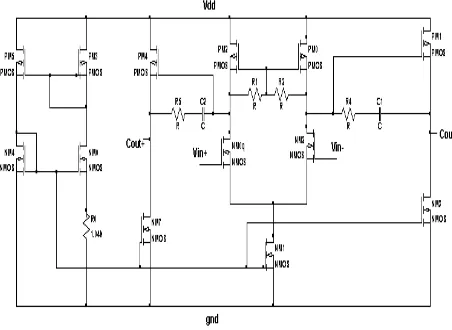
The signal is mainly amplified by NMOS transistors, which have considerable charge carrier mobility. Stage one has the two NMOS differential pair transistorsNM0 and NM2, the respective current source load transistors as PM2 andPM0. NM1 transistor is the tail current source as in Fig.1. The Current source load transistors are gate controlled by a CMFBresistors R1 & R2. These resistors sense the common mode output voltages at the respective drain terminals of NM0 and NM2 input transistors and generate CM output voltage [2]. It is fed to the input of the gates of PM2& PM0. Second stage uses two common source stages as PM4, NM7& PM1, NM5 for differential outputs of first stage in cascade fashion.C1&C2 are used for frequency compensation &the resistors R4& R5 are in series with these C1 and C2 respectively. R4 and R5compensate for the right hand plane zeros generated by C1 and C2. C1 and C2 along with R4 and R5 boost the Gain-Bandwidth and phase margin [2]. The current sourcesNM5 and NM7 of the second stage sink currents as in Fig.1.
III.MODELLING
Fig. 2: Small signal analysis without frequency compensation
Transfer function is given by,
= = ∗ ;(1)
Where, GI, GII are trans-conductanceof first and second stage respectively.
Pole frequencies are given by [6],
p1 =
π
;
(2)
2 = ;(3)
Fig. 3: Small signal analysis with frequency compensation
p1comp =
π( ) ; (5)
Gain Bandwidth can be varied by varying Cc but Cc has got limitation on its varying range as it affects phase margin achieved as well. If resistor Rz is used in series with Cc, a right hand plane zero is turned into left hand plane zero by taking Rz as[1],
> (8)
This condition compensates for more dominant pole. This improves phase margin considerably. Designer can pick up between phase margin and GBW. Phase margin and GBW tradeoff between their performances.
IV.EXPERIMENTAL RESULTS
Opamp is implemented in Cadence Virtuoso analog design environment (ADE) in 45nmprocess in GPDK. DC analysis assures saturation operating conditions of all the MOSFET devices. AC analysis results obtained meet Gain-Bandwidth of 4.23GHz and phase margin of 58.18°.
Fig. 5 First pole
Fig. 6 Second pole
Fig. 8 Gain bandwidth
Fig. 9 Phase margin
First pole is moved to to 15.9MHz and second pole is moved to 5.16 GHz which yields for high phase margin. DC voltage gain is 47 dB. Unity Gain-Bandwidth attained is 4.23GHz. Corner case analysis is also carried out for different corners like typical-typical, slow-slow, fast-fast by degrading supply voltage to 1V and changing operating temperature between -40° to 125 for all these corners.
TABLE I. CIRCUIT PARAMETERS
Parameter Value Comment
Vin 1.1 V Supply
Unity Gain-Bandwidth
4.23GHz -
Idc 715uA DC current
Phase Margin 58.18° -
CL 100fF Off chip load
capacitor
First pole 15.9 MHz -
DC gain 47dB Open loop gain
V. CONCLUSION
All transistors are ensured to be in saturation (region 2). This is carried out with DC analysis. Frequency compensation carried out makes one pole dominant and improves phase margin by separating two poles. Unity gain bandwidth obtained is 4.23 GHz. Phase margin is 58.18°. DC gain achieved is 47dB. C1 and C2 compensating capacitors along with R4 and R5 play key role in phase margin and gain bandwidth achievement. P1 compensated becomes dominant pole as it is very close to origin compared to P1 uncompensated. This opamp is implemented in 45 nm process. Comparison with lower nodes shows that as we scale down in nm regime, more unity GBW can be achieved. Simultaneously, trade off between power consumed and GBW to be achieved should be carefully worked out.
REFERENCES
[1] Alexander Richter, Christoph Tzschoppe, Bastian Lindner, Frank Ellinger, “Low Power High Gain Bandwidth Opamp in Low Cost 180 nm Bulk CMOS Technology,”Microwave and Optoelectronics Conference (IMOC), 2015 SBMO/IEEE MTT-S International, 2015.
[2] Razavi, B. Design of Analog CMOS Integrated Circuits, pp. 314-324.
[3] Abhishek Pandey, Subhra Chakraborty, Suraj Kumar Saw and Vijay Nath, “A Darlington Pair Transistor Based Operational Amplifier,” Proceedings of 2015 Global Conference on Communication Technologies (GCCT 2015), pp. 273- 276, 2015
[4] Daibashish Gangopadhyayand and T. K. Bhattacharyya, “A 2.3 GHz gm-boosted High Swing Class-AB Ultra-Wide Bandwidth Operational Amplifier in 0.18µm CMOS, ”IEEE International Midwest Symposium on Circuits and Systems, pp. 713 - 716, 2010K. Elissa, “Title of paper if known,” unpublished.
[5] S.A EncheAbRahim, MohdAzmi Ismail, Dr. Ahmad Ismat Abdul Rahim, M.R Yahya, Dr. Abdul Fatah Awang Mat, “A Wide Gain-Bandwidth CMOS Fully-Differential Folded Cascode Amplifier,” 2010 International Conference on Electronic Devices, Systems and Applications (ICEDSA2010), pp. 165-168, 2010.
[6] Allen, P. E., &Holberg, D. R. (2002). CMOS analog circuit design. Oxford Univ. Press pp.- 244-272.
[7] S.A EncheAb Rahim, Mohd Azmi Ismail, Dr. Ahmad Ismat Abdul Rahim, M.R Yahya, Dr. Abdul Fatah Awang Mat, “A Wide Gain-Bandwidth CMOS Fully-Differential Folded Cascode Amplifier,” 2010 International Conference on Electronic Devices, Systems and Applications(ICEDSA2010),pp.165-168,2010.
[8] Ehsan Kargaran Hojat Khosrowjerdi and Karim Ghaffarzadegan, “A 1.5 V High Swing Ultra-Low-Power Two Stage CMOS OP-AMP in 0.18µm Technology,”2010 2nd International Conference on Mechanical and Electronics Engineering (ICMEE 2010), pp. vol 1, 68-71, 2010. [9] S.A EncheAb Rahim, Mohd Azmi Ismail, Dr. Ahmad Ismat Abdul Rahim, M.R Yahya, Dr. Abdul Fatah Awang Mat, “A Wide
Gain-Bandwidth CMOS Fully-Differential Folded Cascode Amplifier,” 2010 International Conference on Electronic Devices, Systems and Applications(ICEDSA2010),pp.165-168,2010.
[10] Kamyar Keikhosravy, Pouya Kamalinejad, Shahriar Mirabbasiand Victor Leung, “A Wideband Unity-Gain Buffer in 0.13-μm CMOS”, Electronics, circuits, and systems (ICECS), 2013 IEEE 20thIntternational Conference,pp.9-12,2013.
[11] Sonu Kumar1, Anjali sharma2, Payal Jangra3, Pooja Rathee 4, Rekha Yadav5 “Design of CMOS Operational Amplifier in 180nm Technology” International Journal of Innovative Research in Computer and Communication Engineering Vol. 5, Issue 4, April 2017.