FUNDAMENTALS OF
MICROWAVE
AND RF DESIGN
Michael Steer
Third Edition
ALSO BY THE AUTHOR
Microwave and RF Design
Radio Systems
Volume 1
ISBN 978-1-4696-5690-8
Microwave and RF Design
Transmission Lines
Volume 2
ISBN 978-1-4696-5692-2
Microwave and RF Design
Networks
Volume 3
ISBN 978-1-4696-5694-6
Microwave and RF Design
Modules
Volume 4
ISBN 978-1-4696-5696-0
Microwave and RF Design
Amplifiers and Oscillators
Volume 5
ISBN 978-1-4696-5698-4
FUND
AMENT
ALS OF MICR
O
W
A
VE
AND RF DESIGN
Published by NC State University Distributed by UNC Press
Fundamentals of Microwave and RF Design enables mastery of the essential concepts required to cross the barriers
to a successful career in microwave and RF design. Extensive treatment of scattering parameters, that naturally describe power flow, and of Smith-chart-based design procedures prepare the student for success. The emphasis is on design at the module level and on covering the whole range of microwave functions available. The orientation is towards using microstrip transmission line technologies and on gaining essential mathematical, graphical and design skills for module design proficiency. This book is derived from a multi volume comprehensive book series, Microwave and RF Design, Volumes 1-5, with the emphasis in this book being on presenting the fundamental materials required to gain entry to RF and microwave design. This book closely parallels the companion series that can be consulted for in-depth analysis with referencing of the book series being familiar and welcoming.
KEY FEATURES
• A companion volume to a comprehensive series on microwave and RF design
• Open access ebook editions are hosted by NC State University Libraries at:
https://repository.lib.ncsu.edu/handle/1840.20/36776 • 59 worked examples
• An average of 24 exercises per chapter • Answers to selected exercises
• Emphasis on module-level design using microstrip technologies
• Extensive treatment of design using Smith charts • A parallel companion book series provides a
detailed reference resource
ABOUT THE AUTHOR
Michael Steer is the Lampe Distinguished Professor
of Electrical and Computer Engineering at North Carolina State University. He received his B.E. and Ph.D. degrees in Electrical Engineering from the University of Queensland. He is a Fellow of the IEEE and is a former editor-in-chief of IEEE Transactions on Microwave
Theory and Techniques. He has authored more than 500
Microwave and RF Design
Third Edition
Microwave and RF Design
Third Edition
Michael Steer
Copyright c2019 by M.B. Steer
Citation: Steer, Michael.Fundamentals of Microwave and RF Design. (Third Edi-tion), NC State University, 2019. doi: https//doi.org/10.5149/
9781469656892 Steer
This work is licensed under a Creative Commons Attribution-NonCommercial 4.0 International license (CC BY-NC 4.0). To view a copy of the license, visit http://creativecommons.org/licenses.
ISBN 978-1-4696-5688-5 (paperback)
ISBN 978-1-4696-5689-2 (open access ebook)
Published by NC State University
Distributed by the University of North Carolina Press www.uncpress.org
The objective in writing this textbook is that the student will acquire the skills to be proficient at RF and microwave module design. The distinguishing feature of RF and microwave design is that distributed effects due to the finite delay of electrical signals must be accounted for. Sometimes this requires a design approach that avoids problems due to distributed effects. But very often these effects provide novel circuit functions that have no equivalent at lower frequencies. Distributed effects must be understood so that microwave circuits can be designed to avoid problems such as multimoding. Also understanding distributed effects leads to an understanding and appreciation of the vast trove of unique microwave elements that can be employed in system design. An understanding of microwave network theory will be gained and this leads to development of the skills required to design matched circuits that maximize microwave power transfer. Coupled with filtering, matching maximizes the all important signal-to-interference ratio system metric. Microwave engineering has several ‘barriers-to-entry’ and one of these is the use of graphical techniques in distributed circuit design. The microwave system designer must develop expertise in Smith chart-based design. A second barrier to entry is the need to embrace forward- and backward-traveling waves. This is the way the world works, and the finite speed of information transfer due to signals traveling as electromagnetic waves is a central concept in microwave engineering. This book leaves the design of modules themselves for more specialized microwave design and that is the province of a companion book series.
This book is derived from a multi volume book series with an emphasis in this Fundamentalsbook being on presenting material, the fundamentals, required to cross the threshold to RF and microwave design. The series itself comprises textbooks for several postgraduate classes and is also a comprehensive reference library on microwave engineering. However the series is too detailed for a first course on microwave engineering. But since
The Fundamentals of RF and Microwave Designclosely parallels the book series, referencing the book series will be familiar and welcoming.
The books in the Microwave and RF Design series are authored by Michael Steer, published by North Carolina State University, and distributed by the University of North Carolina Press are:
• Microwave and RF Design: Radio Systems, Volume 1
• Microwave and RF Design: Transmission Lines, Volume 2
• Microwave and RF Design: Networks, Volume 3
• Microwave and RF Design: Modules, Volume 4
• Microwave and RF Design: Amplifiers and Oscillators, Volume 5
As much as possible thisFundamentalsbook parallels the book series using common section names for example. This will help when consulting the series. Even after my many decades in the field, I still fall back on my undergraduate texts as first resources before searching out more detailed and up-to-date information. Perhaps this is because I am well calibrated to these books, and also because one never forgets the first way material is introduced. My hope is that this will also be true for the reader.
Supplementary Materials
Supplementary materials available to qualified instructors adopting the book include PowerPoint slides and solutions to the end-of-chapter problems. Requests should be directed to the author. Access to downloads of the books, additional material and YouTube videos are available at https://www. lib.ncsu.edu/do/open-education
Acknowledgments
Writing this book has been a large task and I am indebted to the many people who helped along the way. First I want to thank the many students at NC State who used drafts and the first two editions. I thank the many instructors and students who have provided feedback. I particularly thank Dr. Wael Fathelbab for advice on , a filter expert, who co-wrote an early version of the filter chapter. Professor Andreas Cangellaris helped in developing the early structure of the book. Many people have reviewed the book and provided suggestions. I thank input on the structure of the manuscript: Professors Mark Wharton and Nuno Carvalho of Universidade de Aveiro, Professors Ed Delp and Saul Gelfand of Purdue University, Professor Lynn Carpenter of Pennsylvania State University, Professor Grant Ellis of the Universiti Teknologi Petronas, Professor Islam Eshrah of Cairo University, Professor Mohammad Essaaidi and Dr. Otman Aghzout of Abdelmalek Essaadi Univeristy, and Professor Jianguo Ma of Guangdong University of Technology. I thank Dr. Jayesh Nath of Apple, Dr. Wael Fathelbab of Northrup Grumman, Mr. Sony Rowland of the U.S. Navy, and Dr. Jonathan Wilkerson of Lawrence Livermore National Laboratories, Dr. Josh Wetherington of Vadum, Dr. Glen Garner of Vadum, and Mr. Justin Lowry who graduated from North Carolina State University.
Many people helped in producing this book. In the first edition I was assisted by Ms. Claire Sideri, Ms. Susan Manning, and Mr. Robert Lawless who assisted in layout and production. The publisher, task master, and chief coordinator, Mr. Dudley Kay, provided focus and tremendous assistance in developing the first and second editions of the book, collecting feedback from many instructors and reviewers. I thank the Institution of Engineering and Technology, who acquired the original publisher, for returning the copyright to me. This open access book was facilitated by John McLeod and Samuel Dalzell of the University of North Carolina Press, and by Micah Vandergrift and William Cross of NC State University Libraries. The open access ebooks are host by NC State University Libraries.
The book was produced using LaTeX and open access fonts, line art was drawn using xfig and inkscape, and images were edited in gimp. So thanks to the many volunteers who developed these packages.
ever imagined. I truly thank them. I also thank my academic sponsor, Dr. Ross Lampe, Jr., whose support of the university and its mission enabled me to pursue high risk and high reward endeavors including this book.
3GPPR is a registered trademark of the European Telecommunications Stan-dards Institute.
802R is a registered trademark of the Institute of Electrical & Electronics En-gineers .
APC-7R is a registered trademark of Amphenol Corporation.
AT&TR is a registered trademark of AT&T Intellectual Property II, L.P. AWRR is a registered trademark of National Instruments Corporation. AWRDER is a trademark of National Instruments Corporation.
BluetoothR is a registered trademark of the Bluetooth Special Interest Group. GSMR is a registered trademark of the GSM MOU Association.
MathcadR is a registered trademark of Parametric Technology Corporation. MATLABR is a registered trademark of The MathWorks, Inc.
NECR is a registered trademark of NEC Corporation.
OFDMAR is a registered trademark of Runcom Technologies Ltd. QualcommR is a registered trademark of Qualcomm Inc.
TeflonR is a registered trademark of E. I. du Pont de Nemours. RFMDR is a registered trademark of RF Micro Devices, Inc. SONNETR is a trademark of Sonnet Corporation.
Smith is a registered trademark of the Institute of Electrical and Electronics Engineers.
Preface . . . v
1 Introduction to Microwave Engineering . . . 1
1.1 RF and Microwave Engineering . . . 1
1.1.1 Electromagnetic Fields . . . 3
1.1.2 Static Field Laws . . . 3
1.1.3 Maxwell’s Equations . . . 5
1.2 Radio Architecture . . . 6
1.3 RF Power Calculations . . . 8
1.3.1 RF Propagation . . . 8
1.3.2 Logarithm . . . 8
1.3.3 Decibels . . . 9
1.4 SI Units . . . 10
1.5 Summary . . . 12
1.6 References . . . 12
1.7 Exercises . . . 13
1.7.1 Exercises By Section . . . 14
1.7.2 Answers to Selected Exercises . . . 14
2 Antennas and the RF Link . . . 15
2.1 Introduction . . . 15
2.2 RF Antennas . . . 16
2.3 Resonant Antennas . . . 17
2.3.1 Radiation from a Current Filament . . . 17
2.3.2 Finite-Length Wire Antennas . . . 19
2.4 Traveling-Wave Antennas . . . 22
2.5 Antenna Parameters . . . 23
2.5.1 Radiation Density and Radiation Intensity . . . 23
2.5.2 Directivity and Antenna Gain . . . 24
2.5.3 Effective Isotropic Radiated Power . . . 27
2.5.4 Effective Aperture Size . . . 27
2.5.5 Summary . . . 28
2.6 The RF Link . . . 28
2.6.1 Propagation Path . . . 29
2.6.2 Resonant Scattering . . . 30
2.6.3 Fading . . . 30
2.6.4 Link Loss and Path Loss . . . 33
2.6.5 Propagation Model in the Mobile Environment . . . . 34
2.7 Antenna Array . . . 35
2.7.1 Multiple Input, Multiple Output . . . 35
2.7.2 Massive MIMO . . . 36
2.8 Summary . . . 37
2.9 References . . . 37
2.10.1 Exercises By Section . . . 40
2.10.2 Answers to Selected Exercises . . . 40
3 Transmission Lines . . . 41
3.1 Introduction . . . 41
3.1.1 When Must a Line be Considered a Transmission Line 42 3.1.2 Movement of a Signal on a Transmission Line . . . 42
3.2 Transmission Line Theory . . . 44
3.2.1 Transmission Line RLGC Model . . . 44
3.2.2 Derivation of Transmission Line Properties . . . 45
3.2.3 Dimensions ofγ,α, andβ . . . 47
3.2.4 Lossless Transmission Line . . . 48
3.2.5 Microstrip Line . . . 48
3.2.6 Summary . . . 49
3.3 The Lossless Terminated Line . . . 50
3.3.1 Total Voltage and Current on the Line . . . 50
3.3.2 Forward- and Backward-Traveling Pulses . . . 52
3.3.3 Input Reflection Coefficient of a Lossless Line . . . 53
3.3.4 Input Impedance of a Lossless Line . . . 55
3.3.5 Standing Waves and Voltage Standing Wave Ratio . . 56
3.3.6 Summary . . . 60
3.4 Special Lossless Line Configurations . . . 60
3.4.1 Short Length of Short-Circuited Line . . . 60
3.4.2 Short Length of Open-Circuited Line . . . 61
3.4.3 Short-Circuited Stub . . . 61
3.4.4 Open-Circuited Stub . . . 63
3.4.5 Electrically Short Lossless Line . . . 64
3.4.6 Quarter-Wave Transformer . . . 66
3.4.7 Summary . . . 67
3.4.8 Summary . . . 67
3.5 Circuit Models of Transmission Lines . . . 67
3.6 Summary . . . 68
3.7 References . . . 68
3.8 Exercises . . . 68
3.8.1 Exercises By Section . . . 70
3.8.2 Answers to Selected Exercises . . . 70
4 Planar Transmission Lines . . . 71
4.1 Introduction . . . 71
4.2 Substrates . . . 72
4.2.1 Dielectric Effect . . . 72
4.2.2 Dielectric Loss Tangent, tanδ . . . 72
4.2.3 Magnetic Material Effect . . . 73
4.2.4 Substrates for Planar Transmission Lines . . . 73
4.3 Planar Transmission Line Structures . . . 74
4.4 Microstrip Transmission Lines . . . 75
4.4.1 Microstrip Line in the Quasi-TEM Approximation . . 75
4.4.2 Effective Permittivity and Characteristic Impedance . 76 4.4.3 Filling Factor . . . 78
4.5 Microstrip Design Formulas . . . 81
4.5.2 Low Impedance . . . 81
4.6 Summary . . . 82
4.7 References . . . 82
4.8 Exercises . . . 82
4.8.1 Exercises by Section . . . 84
4.8.2 Answers to Selected Exercises . . . 84
5 Extraordinary Transmission Line Effects . . . 85
5.1 Introduction . . . 85
5.2 Frequency-Dependent Characteristics . . . 85
5.2.1 Material Dependency . . . 86
5.2.2 Frequency-Dependent Charge Distribution . . . 86
5.2.3 Current Bunching . . . 86
5.2.4 Skin Effect and Internal Conductor Inductance . . . . 88
5.2.5 Skin Effect and Line Resistance . . . 89
5.2.6 Dielectric Dispersion . . . 89
5.2.7 Summary . . . 90
5.3 Multimoding on Transmission Lines . . . 90
5.3.1 Multimoding and Electric and Magnetic Walls . . . 90
5.4 Microstrip Operating Frequency Limitations . . . 93
5.4.1 Microstrip Dielectric Mode (Slab Mode) . . . 93
5.4.2 Higher-Order Microstrip Mode . . . 94
5.4.3 Transverse Microstrip Resonance . . . 95
5.4.4 Summary . . . 96
5.5 Summary . . . 96
5.6 References . . . 96
5.7 Exercises . . . 97
5.7.1 Exercises by Section . . . 98
5.7.2 Answers to Selected Exercises . . . 98
6 Coupled Lines and Applications. . . 99
6.1 Introduction . . . 99
6.2 Physics of Coupling . . . 99
6.2.1 Summary . . . 102
6.3 Low-Frequency Capacitance Model of Coupled Lines . . . 102
6.4 Symmetric Coupled Transmission Lines . . . 104
6.5 Directional Coupler . . . 105
6.5.1 Directional Coupler With Lumped Capacitors . . . 107
6.6 Summary . . . 107
6.7 References . . . 107
6.8 Exercises . . . 108
6.8.1 Exercises by Section . . . 108
6.8.2 Answers to Selected Exercises . . . 108
7 Microwave Network Analysis . . . 109
7.1 Introduction . . . 109
7.2 Two-Port Networks . . . 110
7.2.1 Reciprocity, Symmetry, Passivity, and Linearity . . . . 110
7.2.2 Parameters Based on Total Voltage and Current . . . . 111
7.3 Scattering Parameters . . . 112
7.3.2 Two-PortSParameters . . . 113
7.3.3 Input Reflection Coefficient of a Terminated Two-Port Network . . . 115
7.3.4 Properties of a Two-Port in Terms of S Parameters . . . 116
7.4 Return Loss, Substitution Loss, and Insertion Loss . . . 116
7.4.1 Return Loss . . . 116
7.4.2 Substitution Loss and Insertion Loss . . . 117
7.5 Scattering Parameters and Directional Couplers . . . 118
7.6 Summary . . . 119
7.7 References . . . 120
7.8 Exercises . . . 120
7.8.1 Exercises by Section . . . 121
7.8.2 Answers to Selected Exercises . . . 121
8 Graphical Network Analysis . . . 123
8.1 Introduction . . . 123
8.2 Polar Representations of Scattering Parameters . . . 123
8.2.1 Shift of Reference Planes as a S Parameter Rotation . . 123
8.2.2 Polar Plot of Reflection Coefficient . . . 124
8.3 Smith Chart . . . 124
8.3.1 Impedance Smith Chart . . . 126
8.3.2 Admittance Smith Chart . . . 131
8.3.3 Combined Smith Chart . . . 132
8.3.4 Smith Chart Manipulations . . . 135
8.3.5 An Alternative Admittance Chart . . . 141
8.3.6 Summary . . . 141
8.4 Summary . . . 141
8.5 References . . . 142
8.6 Exercises . . . 142
8.6.1 Exercises by Section . . . 145
8.6.2 Answers to Selected Exercises . . . 145
9 Passive Components. . . 147
9.1 Introduction . . . 147
9.2 QFactor . . . 147
9.2.1 Definition . . . 148
9.2.2 Qof Lumped Elements . . . 149
9.2.3 LoadedQFactor . . . 150
9.2.4 Summary of the Properties ofQ . . . 150
9.3 Surface-Mount Components . . . 150
9.4 Terminations and Attenuators . . . 152
9.4.1 Terminations . . . 152
9.4.2 Attenuators . . . 153
9.5 Transmission Line Stubs and Discontinuities . . . 156
9.5.1 Open . . . 156
9.5.2 Discontinuities . . . 157
9.5.3 Impedance Transformer . . . 158
9.5.4 Planar Radial Stub . . . 158
9.6 Magnetic Transformer . . . 158
9.6.1 Properties of a Magnetic Transformer . . . 158
9.7.1 Marchand Balun . . . 161
9.8 Wilkinson Combiner and Divider . . . 161
9.9 Summary . . . 163
9.10 References . . . 163
9.11 Exercises . . . 164
9.11.1 Exercises by Section . . . 164
9.11.2 Answers to Selected Exercises . . . 164
10 Impedance Matching . . . 165
10.1 Introduction . . . 165
10.2 Matching Networks . . . 165
10.2.1 Matching for Zero Reflection or for Maximum Power Transfer . . . 166
10.2.2 Types of Matching Networks . . . 166
10.3 Impedance Transforming Networks . . . 167
10.3.1 The Ideal Transformer . . . 167
10.3.2 A Series Reactive Element . . . 167
10.3.3 A Parallel Reactive Element . . . 169
10.4 The L Matching Network . . . 169
10.4.1 Design Equations forRS < RL . . . 170
10.4.2 L Network Design forRS> RL . . . 172
10.5 Dealing with Complex Sources and Loads . . . 173
10.5.1 Matching . . . 173
10.6 Multielement Matching . . . 176
10.6.1 Design Concept for Manipulating Bandwidth . . . 176
10.6.2 Three-Element Matching Networks . . . 178
10.6.3 The Pi Network . . . 178
10.6.4 Matching NetworkQRevisited . . . 181
10.6.5 The T Network . . . 182
10.6.6 Broadband (LowQ) Matching . . . 182
10.7 Impedance Matching Using Smith Charts . . . 184
10.7.1 Two-Element Matching . . . 184
10.8 Distributed Matching . . . 188
10.8.1 Stub Matching . . . 190
10.8.2 Hybrid Lumped-Distributed Matching . . . 191
10.9 Matching Options Using the Smith Chart . . . 192
10.9.1 Locating the Design Points . . . 192
10.9.2 Design Options . . . 194
10.9.3 Design 1, Hybrid Design . . . 194
10.9.4 Design 1 with an Open-Circuited Stub . . . 197
10.9.5 Design 2, Lumped-Element Design . . . 198
10.9.6 Summary . . . 200
10.10 Summary . . . 200
10.11 References . . . 201
10.12 Exercises . . . 201
10.12.1 Exercises by Section . . . 204
10.12.2 Answers to Selected Exercises . . . 204
11 RF and Microwave Modules . . . 205
11.1 Introduction to Microwave Modules . . . 205
11.2.1 A 15 GHz Receiver Subsystem . . . 206
11.3 Amplifiers . . . 206
11.4 Filters . . . 209
11.5 Noise . . . 210
11.5.1 Noise Figure . . . 210
11.5.2 Noise of a Cascaded System . . . 212
11.6 Diodes . . . 214
11.7 Switch . . . 215
11.8 Ferrite Components: Circulators and Isolators . . . 218
11.8.1 Gyromagnetic Effect . . . 218
11.8.2 Circulator . . . 218
11.8.3 Circulator Isolation . . . 219
11.8.4 Isolator . . . 219
11.9 Mixer . . . 220
11.10 Local Oscillator . . . 221
11.11 Frequency Multiplier . . . 222
11.12 Summary . . . 222
11.13 References . . . 222
11.14 Exercises . . . 222
11.14.1 Exercises by Section . . . 224
11.14.2 Answers to Selected Exercises . . . 224
Introduction to
Microwave Engineering
1.1 RF and Microwave Engineering . . . 1
1.2 Radio Architecture . . . 6
1.3 RF Power Calculations . . . 8
1.4 SI Units . . . 10
1.5 Summary . . . 12
1.6 References . . . 12
1.7 Exercises . . . 13
1.1
RF and Microwave Engineering
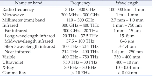
Radio communications is the main driver of RF system development, leading to RF technology evolution at an unprecedented pace. A radio signal is a signal that is coherently generated, radiated by a transmit antenna, propagated through the air, collected by a receive antenna, and then amplified and information extracted. The radio spectrum is part of the electromagnetic (EM) spectrum exploited by humans for communications. A broad categorization of the EM spectrum is shown in Table1-1. Today radios operate from 3 Hz (for submarine communications) to 300 GHz (proposed for 6G cellular communications).
Name or band Frequency Wavelength
Radio frequency 3 Hz – 300 GHz 100 000 km – 1 mm
Microwave 300 MHz – 300 GHz 1 m – 1 mm
Millimeter (mm) band 110 – 300 GHz 2.7 mm – 1.0 mm
Infrared 300 GHz – 400 THz 1 mm – 750 nm
Far infrared 300 GHz – 20 THz 1 mm – 15µm
Long-wavelength infrared 20 THz – 37.5 THz 15–8µm
Mid-wavelength infrared 37.5 – 100 THz 8–3µm
Short-wavelength infrared 100 THz – 214 THz 3–1.4µm
Near infrared 214 THz – 400 THz 1.4µm – 750 nm
Visible 400 THz – 750 THz 750 – 400 mm
Ultraviolet 750 THz – 30 PHz 400 – 10 nm
X-Ray 30 PHz – 30 EHz 10 – 0.01 nm
Gamma Ray >15EHz <0.02nm
Gigahertz, GHz =109
Hz; terahertz, THz =1012
Hz; pentahertz, PHz =1015
Hz; exahertz, EHz =1018Hz.
Figure 1-1: Atmospheric transmis-sion at Mauna Kea, with a height of 4.2 km, on the Island of Hawaii where the atmospheric pressure is 60% of that at sea level and the air is dry with a precipitable water va-por level of 0.001 mm. After [1].
Figure 1-2: Excess attenuation due to atmospheric conditions showing the effect of rain on RF transmission at sea level. Curve (a) is atmospheric at-tenuation, due to excitation of molecular resonances, of very dry air at 0 ◦C, curve (b) is
for typical air (i.e. less dry) at 20◦C. The attenuation shown
for fog and rain is additional (in dB) to the atmospheric ab-sorbtion shown as curve (b).
Propagating RF signals in air are absorbed by molecules in the atmosphere primarily by molecular resonances such as the bending and stretching of bonds which converts EM energy into heat. The transmittance of radio signals versus frequency in dry air at an altitude of 4.2 km is shown in Figure
1-1and there are many transmission holes due to molecular resonances. The lowest frequency molecular resonance in dry air is the oxygen resonance centered at 60 GHz, but below that the absorption in dry air is very small. Attenuation increases with higher water vapor pressure peakin at 22 GHz and broadening due to the close packing of molecules in air. The effect of water is seen in Figure 1-2 and it is seen that rain and water vapor have little effect on cellular communications which are below 5 GHz except for millimeter-wave 5G.
communications is at UHF, 300 MHz to 4 GHz, where antennas are of convenient size and there is a good ability to diffract around objects and even penetrate walls.
1.1.1
Electromagnetic Fields
Communicating using EM signals built from an understanding of magnetic induction based on the experiments of Faraday in 1831 [2] in which he investigated the relationship of magnetic fields and currents, and now known as Faraday’s law. This and the other static field laws are not enough to describe radio waves. The required description is embodied in Maxwell’s equations and after these were developed it took little time before radio was invented.
1.1.2
Static Field Laws
There are two components of the EM field, theelectric field,E, with units of volts per meter (V/m), and themagnetic field,H, with units of amperes per meter (A/m). There are also two flux quantities with the first beingD, theelectric fluxdensity, with units of coulombs per square meter (C/m2), and the other isB, themagnetic fluxdensity, with units of teslas (T).Band H, andDandE, are related to each other by the properties of the medium, which are embodied in the quantitiesµandε(with the caligraphic letter, e.g.
B, denoting a time domain quantity):
¯
B=µH¯ (1.1) D¯ =εE¯, (1.2)
where the over bar denotes a vector quantity, andµis thepermeabilityof the medium and describes the ability to storemagnetic energyin a region. The permeability in free space (or vacuum) isµ0= 4π×10−7H/m and then
¯
B=µ0H¯. (1.3)
The other material quantity is thepermittivity,ε, and in a vacuum
¯
D=ε0E¯, (1.4)
whereε0=8.854×10⁻¹²F/m is the permittivity of a vacuum. Therelative
permittivity,εr, therelative permeability,µr, are defined as
εr=ε/ε0 and µr=µ/µ0. (1.5)
Biot-Savart Law
The Biot–Savart law relates current to magnetic field as, see Figure1-3,
dH¯ = Idℓ׈aR
4πR2 , (1.6)
with units of amperes per meter in the SI system. In Equation (1.6)dH¯ is the incremental staticH field,Iis current,dℓis the vector of the length of a
filament of currentI,aˆR is the unit vector in the direction from the current
filament to the magnetic field, andR is the distance between the filament and the magnetic field. ThedH¯ field is directed at right angles toˆaRand the
Figure 1-3:Diagram illustrat-ing the Biot-Savart law. The law relates a static filament of current to the incrementalH field at a distance.
Figure 1-4: Diagram illustrat-ing Faraday’s law. The contour ℓencloses the surface.
Figure 1-5: Diagram illustrat-ing Ampere’s law. Ampere’s law relates the current, I, on a wire to the magnetic field around it,H.
magnetic field at a point. The total magnetic field from a current on a wire or surface can be found by modeling the wire or surface as a number of current filaments, and the total magnetic field at a point is obtained by integrating the contributions from each filament.
Faraday’s Law of Induction
Faraday’s law relates a time-varying magnetic field to an induced voltage drop,V, around a closed path, which is now understood to be
ℓE ·¯ dℓ, that
is, the closed contour integral of the electric field,
V =
ℓ ¯
E ·dℓ=−
s ∂B¯
∂t ·ds, (1.7)
and this has the units of volts in the SI unit system. The operation described in Equation (1.7) is illustrated in Figure1-4.
Ampere’s Circuital Law
Ampere’s circuital law, often called just Ampere’s law, relates direct current and the static magnetic fieldH¯, see Figure1-5:
ℓ ¯
H·dℓ=Ienclosed. (1.8)
That is, the integral of the magnetic field around a loop is equal to the current enclosed by the loop. Using symmetry, the magnitude of the magnetic field at a distancerfrom the center of the wire shown in Figure1-5is
H =|I|/(2πr). (1.9)
Gauss’s Law
The final static EM law is Gauss’s law, which relates the static electric flux density vector, D¯, to charge. With reference to Figure 1-6, Gauss’s law in integral form is
s ¯ D·ds =
v
ρv·dv=Qenclosed. (1.10)
Figure 1-6: Diagram illustrating Gauss’s law. Charges are distributed in the volume en-closed by the en-closed surface. An incremental area is described by the vector dS, which is normal to the surface and whose magnitude is the area of the incremental area.
Gauss’s Law of Magnetism
Gauss’s law of magnetism parallels Gauss’s law which applies to electric fields and charges. In integral form the law is
s ¯
B·ds = 0. (1.11)
This states that the integral of the constant magnetic flux vector,D¯, over a closed surface is zero reflecting the fact that magnetic charges do not exist.
1.1.3
Maxwell’s Equations
The essential step in the invention of radio was the development of Maxwell’s equations in 1861. Before Maxwell’s equations were postulated, several static EM laws were known. Taken together they cannot describe the propagation of EM signals, but they can be derived from Maxwell’s equa-tions. Maxwell’s equations cannot be derived from the static electric and magnetic field laws. Maxwell’s equations embody additional insight relat-ing spatial derivatives to time derivatives, which leads to a description of propagating fields. Maxwell’s equations are
∇ ×E¯=−∂∂tB¯ −M¯ (1.12)
∇ ·D¯ =ρV (1.13)
∇ ×H¯= ∂D¯
∂t + ¯J (1.14)
∇ ·B¯=ρmV. (1.15)
The additional quantities in Equations (1.12)–(1.15) are
• J¯, the electric current density, with units of amperes per square meter (A/m2);
• ρV, the electric charge density,
with units of coulombs per cubic meter (C/m3);
• ρmV, the magnetic charge
den-sity, with units of webers per cu-bic meter (Wb/m3); and
• M¯, the magnetic current density, with units of volts per square meter (V/m2).
Magnetic charges do not exist, but their introduction through themagnetic chargedensity,ρmV, and themagnetic currentdensity,M¯, introduce an
aes-thetically appealing symmetry to Maxwell’s equations. Maxwell’s equations are differential equations, and as with most differential equations, their so-lution is obtained with particular boundary conditions, which in radio engi-neering are imposed by conductors.
Figure 1-7:A simple transmitter with
low,fLOW, medium,fMED, and high
frequency, fHIGH, sections. The mix-ers can be idealized as multiplimix-ers that boost the frequency of the input base-band or IF signal by the frequency of the carrier.
field. In rectangular coordinates, curl,∇×, describes how much a field circles around thex,y, andzaxes. That is, the curl describes how a field circulates on itself. So Equation (1.12) relates the amount an electric field circulates on itself to changes of theBfield in time. So a spatial derivative of electric fields is related to a time derivative of the magnetic field. Also in Equation (1.14) the spatial derivative of the magnetic field is related to the time derivative of the electric field. These are the key elements that result in self-sustaining propagation.
Div, ∇·, describes how a field spreads out from a point. How fast a field varies with time, ∂B¯/∂t and ∂D¯/∂t, depends on frequency. The more interesting derivatives are ∇ ×E¯ and ∇ ×H¯ which describe how fast a field can change spatially—this depends on wavelength relative to geometry. If the cross-sectional dimensions of a transmission line are less than a wavelength (λ/2 or λ/4 in different circumstances when there are conductors), then it will be impossible for the fields to curl up on themselves and so there will be only one solution (with no or minimal variation of theE andH fields) or, in some cases, no solution to Maxwell’s equations.
1.2
Radio Architecture
A radio device is comprised of reasonably well-defined units, see Figure1-7. The analog baseband signal can have frequency components that range from DC to many megahertz.
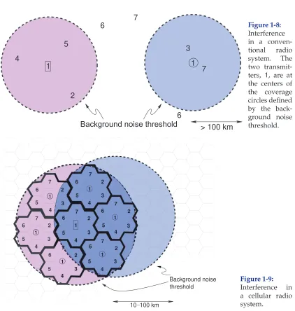
Up until the mid-1970s most wireless communications were based on centralized high-power transmitters and reception was expected until the signal level fell below a noise threshold. These systems were particularly sensitive to interference, therefore systems transmitting at the same frequency were geographically separated so that signals fell below the background noise threshold before there was a chance of interfering with a neighboring system operating at the same frequency. This situation is illustrated in Figure1-8.
Cellular communications is based on the concept of cells in which a terminal unit communicates with a basestation at the center of a cell. For communication in closely spaced cells to work, interference from other radios must be managed. This is facilitated using the ability to recover from errors available with error correction schemes.
Figure 1-8:
Interference in a conven-tional radio
system. The
two transmit-ters, 1, are at the centers of the coverage circles defined by the back-ground noise threshold.
Figure 1-9:
Interference in a cellular radio system.
a cluster and the full set is repeated in each cluster, e.g. in Figure1-9a 7-cell cluster is shown; and (b) frequency reuse. with frequencies used in one cell are reused in the corresponding cell in another cluster. As the cells are relatively close, it is important to dynamically control the power radiated by each radio, as radios in one cell will produce interference in other clusters.
1.3
RF Power Calculations
1.3.1
RF Propagation
As an RF signal propagates away from a transmitter the power density reduces conserving the power in the EM wave. In the absence of obstacles and without atmospheric attenuation the total power passing through the surface of a sphere centered on a transmitter is equal to the power transmitted. Since the area of the sphere of radius r is 4πr2, the power density, e.g. in W/m2, at a distance rdrops off as1/r2. With obstacles the EM wave can be further attenuated.
EXAMPLE 1.1 Signal Propagation
A signal is received at a distancerfrom a transmitter and the received power drops off as
1/r2. Whenr= 1km, 100 nW is received. What isrwhen the received power is 100 fW?
Solution:
The signal collected by the receiver is proportional to the power density of the EM signal. The received signal powerPr=k/r2wherekis a constant. This leads to
Pr(1 km)
Pr(r) =
100 nW 100 fW = 10
6
= kr
2
k(1 km)2 = r2
(103m)2; r =
√
1012m2= 1000 km (1.16)
1.3.2
Logarithm
A cellular phone can reliably receive a signal as small as 100 fW and the signal to be transmitted could be 1 W. So the same circuitry can encounter signals differing in power by a factor of1013. To handle such a large range of signals a logarithmic scale is used.
Logarithms are used in RF engineering to express the ratio of powers using reasonable numbers. Logarithms are taken with respect to a basebsuch that ifx=by, theny= log
b(x). In engineering,log(x)is the same aslog10(x), and
ln(x)is the same asloge(x)and is called the natural logarithm (e = 2.71828 . . . ). In physics and mathematics logx (and programs such as MATLAB) meanslnx, so be careful. Common formulas involving logarithms are given in Table1-2.
Table 1-2:Common logarithm formulas. In engineeringlogx≡log10xandlnx≡log2x.
Description Formula Example
Equivalence y= logb(x)←→x=by log(1000) = 3
and103= 1000
Product logb(xy) = logb(x) + logb(y) log(0.13·978) = log(0.13) + log(978) =−0.8861 + 2.990 = 2.104
Ratio logb(x/y) = logb(x)−logb(y) ln(8/2) = ln(8)−ln(2) = 3−1 = 2
Power logb(xp) =plogb(x) ln
32
= 2 ln (3) = 2·1.0986 = 2.197
Root logb(p
√
x) =1plogb(x) log
√3
20
=13log(20) = 0.4337
Change
of base logb(x) =
logk(x)
logk(b) ln(100) =
log(100) log(2) =
2
1.3.3
Decibels
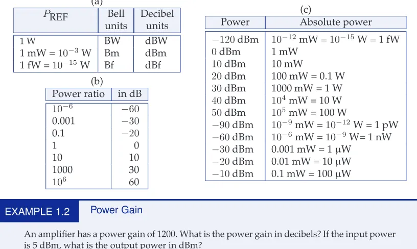
RF signal levels are expressed in terms of the power of a signal. While power can be expressed in absolute terms, e.g. watts (W), it is more useful to use a logarithmic scale. The ratio of two power levelsP andPREFin bels (B) is
P(B) = log
P PREF
, (1.17)
wherePREF is a reference power. Herelogxis the same aslog10x. Human senses have a logarithmic response and the minimum resolution tends to be about 0.1 B, so it is most common to use decibels (dB); 1 B = 10 dB. Common designations are shown in Table1-3. Also, 1 mW = 0 dBm is a very common power level in RF and microwave power circuits where the m in dBm refers to the 1 mW reference. As well, dBW is used, and this is the power ratio with respect to 1 W with 1 W = 0 dBW = 30 dBm.
Table 1-3: Common power designations: (a) reference powers, PREF; (b) power ratios in decibels(dB); and (c) powers in dBm and watts.
(a)
PREF Bell Decibel
units units
1 W BW dBW
1 mW =10−3W Bm dBm
1 fW =10−15W Bf dBf
(b)
Power ratio in dB
10−6 −60
0.001 −30
0.1 −20
1 0
10 10
1000 30
106 60
(c)
Power Absolute power
−120dBm 10−12mW =10−15W = 1 fW
0dBm 1 mW
10dBm 10 mW
20dBm 100 mW = 0.1 W
30dBm 1000 mW = 1 W
40dBm 104mW = 10 W
50dBm 105mW = 100 W
−90dBm 10−9mW =10−12W = 1 pW
−60dBm 10−6mW =10−9W= 1 nW
−30dBm 0.001 mW = 1µW
−20dBm 0.01 mW = 10µW
−10dBm 0.1 mW = 100µW
EXAMPLE 1.2 Power Gain
An amplifier has a power gain of 1200. What is the power gain in decibels? If the input power is 5 dBm, what is the output power in dBm?
Solution:
Power gain in decibels,GdB= 10 log 1200 = 30.79 dB.
The output power isPout|dBm=PdB+Pin|dBm= 30.79 + 5 = 35.79 dBm.
EXAMPLE 1.3 Gain Calculations
A signal with a power of 2 mW is applied to the input of an amplifier that increases the power of the signal by a factor of 20. (a) What is the input power in dBm?
Pin= 2 mW = 10·log
2 mW 1 mW
(b) What is the gain,G, of the amplifier in dB?
The amplifier gain (by default this is power gain) is
G= 20 = 10·log(20) dB = 10·1.301 dB = 13.0 dB. (1.19) (c) What is the output power of the amplifier?
G=Pout
Pin
, and in decibels G|dB= Pout|dBm−Pin|dBm (1.20)
Thus the output power in dBm is
Pout|dBm= G|dB+Pin|dBm= 13.0 dB + 3.0 dBm = 16.0 dBm. (1.21)
Note that dB and dBm are dimensionless but they do have meaning; dB indicates a power ratio but dBm refers to a power. Quantities in dB and one quantity in dBm can be added or subtracted to yield dBm, and the difference of two quantities in dBm yields a power ratio in dB.
In Examples 1.2 and 1.3 two digits following the decimal point were used for the output power expressed in dBm. This corresponds to an implied accuracy of about 0.01% or 4 significant digits of the absolute number. This level of precision is typical for the result of an engineering calculation.
EXAMPLE 1.4 Power Calculations
The output stage of an RF front end consists of an amplifier followed by a filter and then an antenna. The amplifier has a gain of 33 dB, the filter has a loss of 2.2 dB, and of the power input to the antenna, 45% is lost as heat due to resistive losses. If the power input to the amplifier is 1 W, then:
(a) What is the power input to the amplifier expressed in dBm?
Pin= 1 W = 1000 mW, PdBm= 10 log(1000/1) = 30 dBm.
(b) Express the loss of the antenna in dB.
45% of the power input to the antenna is dissipated as heat. The antenna has an efficiency,η, of 55% and soP2= 0.55P1.
Loss =P1/P2= 1/0.55 = 1.818 = 2.60dB.
(c) What is the total gain of the RF front end (amplifier + filter + antenna)?
Total gain = (amplifier gain)dB+ (filter gain)dB−(loss of antenna)dB
= (33−2.2−2.6) dB = 28.2 dB (1.22) (d) What is the total power radiated by the antenna in dBm?
PR=Pin|dBm+ (amplifier gain)dB+ (filter gain)dB−(loss of antenna)dB
= 30 dBm + (33−2.2−2.6) dB = 58.2 dBm. (1.23) (e) What is the total power radiated by the antenna?
PR= 1058.2/10= (661×103) mW = 661 W. (1.24)
1.4
SI Units
The main SI units used in microwave engineering are given in Table1-4.
Table 1-4:Main SI units used in RF and microwave engineering.
SI unit Name Usage In terms of fundamental units
A ampere current (abbreviated as amp) Fundamental unit
cd candela luminous intensity Fundamental unit
C coulomb charge A·s
F farad capacitance kg−1·m−2·A−2·s4
g gram weight =kg/1000
H henry inductance kg·m2·A−2·s−2
J joule unit of energy kg·m2·s−2
K kelvin thermodynamic temperature Fundamental unit
kg kilogram SI fundamental unit Fundamental unit
m meter length Fundamental unit
mol mole amount of substance Fundamental unit
N newton unit of force kg·m·s−2
Ω ohm resistance kg·m2·A−2·s−3
Pa pascal pressure kg·m−1·s−2
s second time Fundamental unit
S siemen admittance kg−1·m−2·A2·s3
V volt voltage kg·m2·A−1·s−3
W watt power J·s−1
• A space separates a value from the symbol for the unit (e.g., 5.6 kg). There is an exception for degrees, with the symbol◦, e.g.45◦.
When SI units are multiplied a center dot is used. For example, newton meters is written N·m. When a unit is derived from the ratio of symbols then either a solidus (/) or a negative exponent is used; the symbol for velocity (meters per second) is either m/s orm·s−1. The use of multiple solidi for a combination symbol is confusing and must be avoided. So the symbol for acceleration ism·s−2or m/s2and not m/s/s.
Consider calculation of the thermal resistance of a rod of cross-sectional areaAand lengthℓ:
RTH= ℓ
kA. (1.25)
IfA= 0.3 cm2andℓ= 2mm, the thermal resistance is
RTH=
(2 mm)
(237 kW·m−1·K−1)·(0.3 cm2)
= (2·10
−3m)
237·(103·W·m−1·K−1)·0.3·(10−2·m)2
= 2·10
−3
237·103·0.3·10−4·
m W·m−1·K−1·m2
= 2.813·10−4K·W−1= 281.3µK/W. (1.26)
This would be an error-prone calculation if the thermal conductivity was taken as 237 kW/m/K.
of the prefixes for bits and bytes were adopted [3] removing the confusion over the earlier use of quantities such as kilobit to represent either 1,000 bits or 1,024 bits. Now kilobit (kbit) always means 1,000 bits and a new term kibibit (Kibit) means 1,024 bit. Also the now obsolete usage of kbps is replaced by kbit/s (kilobit per second). The prefix k stands for kilo (i.e. 1,000) and Ki is the symbol for the binary prefix kibi- (i.e. 1,024). The symbol for byte (= 8 bits) is “B”.
Table 1-5:SI prefixes.
SI Prefixes Symbol Factor Name
10−24 y yocto
10−21
z zepto
10−18 a atto
10−15
f femto
10−12 p pico
10−9 n nano
10−6 µ micro
10−3 m milli
10−2
c centi
10−1 d deci
SI Prefixes Symbol Factor Name
101 da deca
102
h hecto
103 k kilo
106
M mega
109 G giga
1012 T tera
1015 P peta
1018 E exa
1021
Z zetta
1024 Y yotta
Prefixes for bits and bytes Name
kilobit kbit 1000 bit megabit Mbit 1000 kbit
gigabit Gbit 1000 Mbit terabit Tbit 1000 Gbit kibibit Kibit 1024 bit mebibit Mibit 1024 Kibit
gibibit Gibit 1024 Mibit tebibit Tibit 1024 Gibit kilobyte kB 1000 B kibibyte KiB 1024 B
1.5
Summary
The RF spectrum is used to support a tremendous range of applications, including voice and data communications, satellite-based navigation, radar, weather radar, mapping, environmental monitoring, air traffic control, police radar, perimeter surveillance, automobile collision avoidance, and many military applications.
In RF and microwave engineering there are always considerable approximations made in design, partly because of necessary simplifications that must be made in modeling, but also because many of the material properties required in a detailed design can only be approximately known. Most RF and microwave design deals with frequency-selective circuits often relying on line lengths that have a length that is a particular fraction of a wavelength. Many designs can require frequency tolerances of as little as 0.1%, and filters can require even tighter tolerances. It is therefore impossible to design exactly. Measurements are required to validate and iterate designs. Conceptual understanding is essential; the designer must be able to relate measurements, which themselves have errors, with computer simulations. The ability to design circuits with good tolerance to manufacturing variations and perhaps circuits that can be tuned by automatic equipment are skills developed by experienced designers.
1.6
References
[1] “Atmospheric microwave transmittance at mauna kea, wikipedia creative commons.” [2] “IEEE Virtual Museum,” at
http://www.ieee-virtual-museum.org Search term: ‘Faraday’.
1.7
Exercises
1. What is the wavelength in free space of a signal at 4.5 GHz?
2. Consider a monopole antenna that is a quarter of a wavelength long. How long is the antenna if it operates at 3 kHz?
3. Consider a monopole antenna that is a quarter of a wavelength long. How long is the antenna if it operates at 500 MHz?
4. Consider a monopole antenna that is a quarter of a wavelength long. How long is the antenna if it operates at 2 GHz?
5. A dipole antenna is half of a wavelength long. How long is the antenna at 2 GHz?
6. A dipole antenna is half of a wavelength long. How long is the antenna at 1 THz?
7. A transmitter transmits an FM signal with a bandwidth of 100 kHz and the signal is received by a receiver at a distancerfrom the transmitter. Whenr = 1km the signal power received by the receiver is 100 nW. When the receiver moves further away from the transmitter the power re-ceived drops off as1/r2
. What isrin kilometers when the received power is 100 pW. [Parallels Example 1.1]
8. A transmitter transmits an AM signal with a bandwidth of 20 kHz and the signal is received by a receiver at a distancerfrom the transmitter. Whenr= 10km the signal power received is 10 nW. When the receiver moves further away from the transmitter the power received drops off as
1/r2. What isrin kilometers when the received power is equal to the received noise power of 1 pW? [Parallels Example 1.1]
9. The logarithm to base 2 of a numberxis 0.38 (i.e.,log2(x) = 0.38). What isx?
10. The natural logarithm of a numberxis 2.5 (i.e.,
ln(x) = 2.5). What isx?
11. The logarithm to base 2 of a numberxis 3 (i.e.,
log2(x) = 3). What islog2(2
√
x)? 12. What islog3(10)?
13. What islog4.5(2)?
14. Without using a calculator evaluate
log{[log3(3x)−log3(x)]}.
15. A 50Ωresistor has a sinusoidal voltage across it with a peak voltage of 0.1 V. The RF voltage is
0.1 cos(ωt), whereωis the radian frequency of the signal andtis time.
(a) What is the power dissipated in the resistor in watts?
(b) What is the power dissipated in the resistor in dBm?
16. The power of an RF signal is 10 mW. What is the power of the signal in dBm?
17. The power of an RF signal is 40 dBm. What is the power of the signal in watts?
18. An amplifier has a power gain of 2100. (a) What is the power gain in decibels? (b) If the input power is−5dBm, what is the
output power in dBm? [Parallels Example 1.2]
19. An amplifier has a power gain of 6. What is the power gain in decibels? [Parallels Example 1.2] 20. A filter has a loss factor of 100. [Parallels
Exam-ple 1.2]
(a) What is the loss in decibels? (b) What is the gain in decibels?
21. An amplifier has a power gain of 1000. What is the power gain in dB? [Parallels Example 1.2] 22. An amplifier has a gain of 14 dB. The input to
the amplifier is a 1 mW signal, what is the out-put power in dBm?
23. An RF transmitter consists of an amplifier with a gain of 20 dB, a filter with a loss of 3 dB and then that is then followed by a lossless transmit antenna. If the power input to the amplifier is 1 mW, what is the total power radiated by the antenna in dBm? [Parallels Example 1.4] 24. The final stage of an RF transmitter consists of an
amplifier with a gain of 30 dB and a filter with a loss of 2 dB that is then followed by a transmit antenna that looses half of the RF power as heat. [Parallels Example 1.4]
(a) If the power input to the amplifier is 10 mW, what is the total power radiated by the an-tenna in dBm?
(b) What is the radiated power in watts? 25. A 5 mW-RF signal is applied to an amplifier that
increases the power of the RF signal by a factor of 200. The amplifier is followed by a filter that losses half of the power as heat.
(a) What is the output power of the filter in watts?
(b) What is the output power of the filter in dBW?
26. The power of an RF signal at the output of a re-ceive amplifier is 1µW and the noise power at
27. The power of a received signal is 1 pW and the received noise power is 200 fW. In addition the level of the interfering signal is 100 fW. What is the signal-to-noise ratio in dB? Treat interference as if it is an additional noise signal.age gain of 1 has an input impedance of100 Ω, a zero output impedance, and drives a5 Ωload. What is the power gain of the amplifier?
28. A transmitter transmits an FM signal with a bandwidth of 100 kHz and the signal power re-ceived by a receiver is 100 nW. In the same band-width as that of the signal the receiver receives 100 pW of noise power. In decibels, what is the ratio of the signal power to the noise power, i.e. the signal-to-noise ratio (SNR) received by the receiver?
29. An amplifier with a voltage gain of 20 has an in-put resistance of100 Ωand an output resistance of50 Ω. What is the power gain of the amplifier in decibels? [Parallels Example 1.0]
30. An amplifier with a voltage gain of 1 has an in-put resistance of100 Ωand an output resistance of5 Ω. What is the power gain of the amplifier in decibels? Explain why there is a power gain of more than 1 even though the voltage gain is 1. [Parallels Example 1.0]
31. An amplifier has a power gain of 1900. (a) What is the power gain in decibels?
(b) If the input power is−8dBm, what is the output power in dBm? [Parallels Example 1.2]
32. An amplifier has a power gain of 20. (a) What is the power gain in decibels?
(b) If the input power is−23dBm, what is the output power in dBm? [Parallels Example 1.2]
33. An amplifier has a voltage gain of 10 and a cur-rent gain of 100.
(a) What is the power gain as an absolute num-ber?
(b) What is the power gain in decibels? (c) If the input power is−30dBm, what is the
output power in dBm?
(c) What is the output power in mW?
34. An amplifier with 50 Ω input impedance and 50Ωload impedance has a voltage gain of 100. What is the (power) gain in decibels?
35. An attenuator reduces the power level of a sig-nal by 75%. What is the (power) gain of the at-tenuator in decibels?
1.7.1
Exercises By Section
†challenging
§1.2 1,2,3,4,5,6,7,8
§1.3 9,10,11,12,13,14,15,16,17
18,19,20,21,22,23†,24†,25†
26,27,28,29,30,31,32,33,34,35
1.7.2
Answers to Selected Exercises
4 3.25 cm 12 2.096 16 10 dBm
17 10 W 19 7.782 dB 22 1.301
Antennas and the RF Link
2.1 Introduction . . . 15 2.2 RF Antennas . . . 16 2.3 Resonant Antennas . . . 17 2.4 Traveling-Wave Antennas . . . 22 2.5 Antenna Parameters . . . 23 2.6 The RF link . . . 28 2.7 Antenna array . . . 35 2.8 Summary . . . 37 2.9 References . . . 37 2.10 Exercises . . . 38
2.1
Introduction
An antenna interfaces circuits with free-space with a transmit antenna converting a guided wave signal on a transmission line to an electromagnetic (EM) wave propagating in free space, while a receive antenna is a transducer that converts a free-space EM wave to a guided wave on a transmission line and eventually to a receiver circuit. Together the transmit and receive antennas are part of the RF link. The RF link is the path between the output of the transmitter circuit and the input of the receiver circuit (see Figure 2-1). Usually this path includes the cable from the transmitter to the transmit antenna, the transmit antenna itself, the propagation path, the receive antenna, and the transmission line connecting the receive antenna to the receiver circuit. The received signal is much smaller than the transmitted signal. The overwhelming majority of the loss is from the propagation path as the EM signal spreads out, and usually diffracts, reflects, and is partially blocked by objects such as hills and buildings.
Figure 2-1:RF link.
(b) Microstrip patch antenna
(a) Monopole antenna (c) Vivaldi antenna
Figure 2-2:Representative resonant, (a) and (b), and traveling-wave, (c), antennas.
EXAMPLE 2.1 Interference
In the figure there are two transmitters, Tx1and Tx2, operating
at the same power level, and one receiver, Rx. Tx1 is an
intentional transmitter and its signal is intended to be received at Rx. Tx1 is separated from Rx byD1 = 2km. Tx2 uses the
same frequency channel as Tx1, and as far as RX is concerned
it transmits an interfering signal. Assume that the antennas are omnidirectional (i.e., they transmit and receive signals equally in all directions) and that the transmitted power density drops off as 1/d2, where d is the distance from the transmitter.
Calculate the signal-to-interference ratio (SIR) at Rx.
Solution:
D1= 2 kmandD2= 4 km.
P1is the signal power transmitted by Tx1 and received at Rx. P2is the interference power transmitted by Tx2 and received at Rx.
So SIR=P1
P2
=
D2 D1
2
= 4 = 6.02 dB.
2.2
RF Antennas
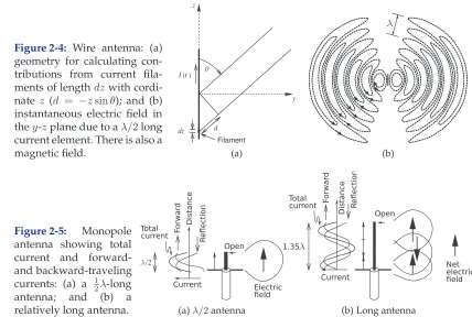
(a) Current filament (h≪λ) (b) Half-wavelength long wire
Figure 2-3:Wire antennas. The distance from the cen-ter of an antenna to the field pointP isr.
R=rsinθ.
of an antenna, charges, i.e. free electrons, accelerate or decelerate under the influence of an applied voltage source which typically arrives at the antenna from a traveling wave voltage on a transmission line. When the charges accelerate (or decelerate) they produce an EM field which radiates away from the antenna. At a point on the antenna there is a current sinusoidally varying in time, and the net acceleration of the charges (in charge per second per second) is also sinusoidal with an amplitude that is directly proportional to the amplitude of the current sinewave. Hence having a large standing wave of current, when the antenna resonates sinusoidally, results in a large charge acceleration and hence large radiated fields.
When an EM field impinges upon a conductor the field causes charges to accelerate and hence induce a voltage that propagates on a transmission line connected to the receive antenna. Traveling-wave antennas, an example of one is shown in Figures2-2(c), operate as extended lines that gradually flare out so that a traveling wave on the original transmission line transitions into free space. Traveling-wave antennas tend to be two or more wavelengths long at the lowest frequency of operation. While relatively long, they are broadband, many 3 or more octaves wide (e.g. extending from 500 MHz to 4 GHz or more). These antennas are sometimes referred to asaperture antennas.
2.3
Resonant Antennas
With a resonant antenna the current on the antenna is directly related to the amplitude of the radiated EM field. Resonance ensures that the standing wave current on the antenna is high.
2.3.1
Radiation from a Current Filament
dimensions, that is, it is considered to be infinitely thin.
Resonant antennas are conveniently modeled as being made up of an array of current filaments with spacings and lengths being a tiny fraction of a wavelength. Wire antennas are even simpler and can be considered to be a line of current filaments. Ramo, Whinnery, and Van Duzer [1] calculated the spherical EM fields at the pointP with the spherical coordinates(φ, θ, r)
generated by thez-directed current filament centered at the origin in Figure
2-3. The total EM field components in phasor form are
Hφ= I0h 4πe
−kr k r + 1 r2
sinθ, H¯φ=Hφφˆ (2.1)
Er= I0h 4πe
−kr
2η r2 +
2 ωε0r3
cosθ, E¯r=Erˆr (2.2)
Eθ= I0h 4πe
−kr
ωµ0 r +
1 ωε0r3 +
η r2
sinθ, E¯θ=Eθθ,ˆ (2.3)
whereηis the free-space characteristic impedance. The variablekis called the wavenumberand k = 2π/λ = ω√µ0ε0. The e−kr terms describe the variation of the phase of the field as the field propagates away from the filament. Equations (2.1)–(2.3) are the complete fields with the1/r2and1/r3 dependence describing the near-field components. In the far field, i.e.r≫λ, the components with1/r2and1/r3dependence become negligible and the field components left are the propagating componentsHφandEθ:
Hφ= I0h
4πe
−krk r
sinθ, Er= 0, and Eθ= I0h
4πe
−krωµ0 r
sinθ.
(2.4)
Now consider the fields in the plane normal to the filament, that is, with θ=π/2radians so thatsinθ= 1. The fields are now
Hφ=I0h 4πe
−kr
k r
and Eθ= I0h 4πe
−krωµ0 r
(2.5)
and the wave impedance is
η= Eθ Hφ
= I0h 4πe
−krωµ0 r
I0h
4πe
−krk r
−1
=ωµ0
k . (2.6)
Note that the strength of the fields is directly proportional to the magnitude of the current. This proves to be very useful in understanding spurious radiation from microwave structures. Nowk=ω√µ0ǫ0, so
η= ωµ0 ω√µ0ǫ0
=
µ
0 ǫ0
= 377 Ω, (2.7)
as expected. Thus an antenna can be viewed as having the inherent function of an impedance transformer converting from the lower characteristic impedance of a transmission line (often 50 Ω) to the 377 Ω characteristic impedance of free space.
line with the filament. For fixedr, the amplitude of the propagating field increases sinusoidally with respect toθuntil it is maximum in the direction normal to the filament.
The power radiated is obtained using thePoynting vector, which is the cross-product of the propagating electric and magnetic fields. From this the time-average propagating power density is (with the SI units ofW/m2)
PR= 1 2ℜ
EθHφ∗
=ηk
2|I
0|2h2
32π2r2 sin
2θ, (2.8)
and the power density is proportional to 1/r2. In Equation (2.8) ℜ(· · ·)
indicates that the real part is taken.
2.3.2
Finite-Length Wire Antennas
The EM wave propagated from a wire of finite length is obtained by considering the wire as being made up of many filaments and the field is then the superposition of the fields from each filament. As an example, consider the antenna in Figure2-3(b) where the wire is half a wavelength long. As a good approximation the current on the wire is a standing wave and the current on the wire is in phase so that the current phasor is
I(z) =I0cos(kz). (2.9)
From Equation (2.4) and referring to Figure2-3the fields in the far field are
Hφ=
λ/4
−λ/4
I0cos(kz)
4π e
−kr′k
r′
sinθ′dz (2.10)
Eθ=
λ/4
−λ/4
I0cos(kz)
4π e
−kr′ωµ0
r′
sinθ′ dz, (2.11)
whereθ′is the angle from the filament to the pointP. Nowk= 2π/λand at
the ends of the wirez =±λ/4wherecos(kz) = cos(±π/2) = 0. Evaluating the equations is analytically involved and will not be done here. The net result is that the fields are further concentrated in the plane normal to the wire. At larger, of at least several wavelengths distant from the antenna, only the field components decreasing as1/r are significant. At larger the phase differences of the contributions from the filaments is significant and results in shaping of the fields. The geometry to be used in calculating the far field is shown in Figure2-4(a). The phase contribution of each filament, relative to that atz= 0, is(kzsinθ)/λand Equations (2.10) and (2.11) become
Hφ=I0
k
4πr
sin(θ) e−kr λ/4
−λ/4
sin(kz)
4π sin(zsin(θ))dz (2.12)
Eθ=I0 ωµ0
4πr
sin(θ) e−kr
λ/4
−λ/4
sin(kz) sin(zsin(θ))dz. (2.13)
Figure 2-4(b) is a plot of the near-field electric field in the y-z plane calculating Er and Eθ (recall that Eφ = 0) every 90◦. Further from the
antenna theErcomponent rapidly reduces in size, andEθdominates.
Figure 2-4: Wire antenna: (a) geometry for calculating con-tributions from current fila-ments of lengthdzwith cordi-nate z (d = −zsinθ); and (b) instantaneous electric field in they-zplane due to aλ/2long current element. There is also a
magnetic field. (a) (b)
Figure 2-5: Monopole antenna showing total current and forward-and backward-traveling currents: (a) a 12λ-long
antenna; and (b) a
relatively long antenna. (a)λ/2antenna (b) Long antenna
current on the wire antenna. So establishing a standing current wave and hence magnifying the current is important to the efficiency of a wire antenna. A second result is that the power density of freely propagating EM fields in the far field is proportional to1/r2, whereris the distance from the antenna. A third interpretation is that the longer the antenna, the flatter the radiated transmission profile; that is, the radiated energy is more tightly confined to thex-y (i.e. Θ = 0) plane. For the wire antenna the peak radiated field is in the plane normal to the antenna, and thus the wire antenna is generally oriented vertically so that transmission is in the plane of the earth and power is not radiated unnecessarily into the ground or into the sky.
To obtain an efficient resonant antenna, all of the current should be pointed in the same direction at a particular time. One way of achieving this is to establish a standing wave, as shown in Figure2-5(a). At the open-circuited end, the current reflects so that the total current at the end of the wire is zero. The initial and reflected current waves combine to create a standing wave. Provided that the antenna is sufficiently short, all of the total current— the standing wave—is pointed in the same direction. The optimum length is about a half wavelength. If the wire is longer, the contributions to the field from the oppositely directed current segments cancel (see Figure2-5(b)).
Figure 2-6:Mobile antenna with phas-ing coil extendphas-ing the effective length of the antenna.
(a) (b) (c)
Figure 2-7:Dipole antenna: (a) current distribution; (b) stacked dipole antenna; and (c) detail of the connection in a stacked dipole antenna.
be directly connected to the antenna and there is only a small mismatch and nearly all the power is transferred to the antenna and then radiated.
Another variation on the monopole is shown in Figure2-6, where the key component is the phasing coil. The phasing coil (with a wire length ofλ/2) rotates the electrical angle of the current phasor on the line so that the current on theλ/4segment is in the same direction as on theλ/2segment. The result is that the two straight segments of the loaded monopole radiate a more tightly confined EM field. The phasing coil itself does not radiate (much).
Another ingenious solution to obtaining a longer effective wire antenna with same-directed current (and hence a more tightly confined RF beam) is the stacked dipole antenna (Figure2-7). The basis of the antenna is a dipole as shown in Figure 2-7(a). The cable has two conductors that have equal amplitude currents,I, but flowing as shown. The wire section is coupled to the cable so that the currents on the two conductors realize a single effective currentIdipole on the dipole antenna. The stacked dipole shown in Figure
(a)
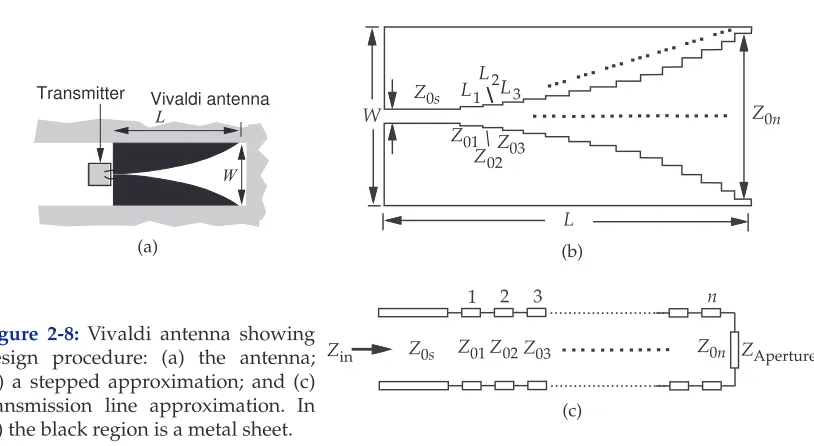
Figure 2-8: Vivaldi antenna showing design procedure: (a) the antenna; (b) a stepped approximation; and (c) transmission line approximation. In (a) the black region is a metal sheet.
(b)
(c)
Summary
Standing waves of current can be realized by resonant structures other than wires. A microstrip patch antenna, see Figure 2-2(b), is an example, but the underlying principle is that an array of current filaments generates EM components that combine to create a propagating field. Resonant antennas are inherently narrowband because of the reliance on the establishment of a standing wave. A relative bandwidth of 5%–10% is typical.
2.4
Traveling-Wave Antennas
Traveling-wave antennas have the characteristics of broad bandwidth and large size. These antennas begin as a transmission line structure that flares out slowly, providing a low reflection transition from a transmission line to free space. The bandwidth can be very large and is primarily dependent on how gradual the transition is.
One of the more interesting traveling-wave antennas is the Vivaldi antennaof Figure2-8(a). The Vivaldi antenna is an extension of a slotline in which the fields are confined in the space between two metal sheets in the same plane. The slotline spacing increases gradually in an exponential manner, much like that of a Vivaldi violin (from which it gets its name), over a distance of a wavelength or more. A circuit model is shown in Figures2-8(b and c) where the antenna is modeled as a cascade of many transmission lines of slowly increasing characteristic impedance,Z0. Since theZ0progression is gradual there are low-level reflections at the transmission line interfaces. The forward-traveling wave on the antenna continues to propagate with a negligible reflected field. Eventually the slot opens sufficiently that the effective impedance of the slot is that of free space and the traveling wave continues to propagate in air.