ABSTRACT
LI, XIAODONG. Modeling and Simulation of Electron Transport Properties of Novel Two Dimensional Electron Systems. (Under the direction of Prof. Ki Wook Kim.)
In the past decade, a lot of research work have been focusing on the two-dimensional materi-als, such graphene, silicene, atomic thin layer transitional metal dichalcogenides (MoS2, MoSe2, WS2, etc), and topological insulators (Bi2Se3, Bi2Te3, etc), due to their novel properties in condense-matter physics, and potential applications in electronics and optics. In this work, the electron transport properties of selected materials are investigated theoretically, together with the analysis of the effects on the performance of semiconductor devices. Graphene and its deriva-tive, bilayer graphene, are chosen to be our first two research objects. A full band Monte Carlo simulation program is developed to investigate the electron transport properties, including var-ious scattering mechanisms and the influence of the substrates. Secondly, the electron-phonon interaction in monolayer silicene and MoS2 are studied from first principles as well as the intrin-sic electron transport. Then, for three dimensional topological insulators, the exotic properties of the spin-polarized surface states have drawn huge attentions among the scientists. In partic-ular, for our work, the electron wave guiding phenomena on the surface within the proximate of the magnetic layer are investigated with the proposal of several potential applications in logic device and interconnect circuits.
through interfacial thermal conducting and energy transferring to substrate by surface polar phonon scattering. Considering the overall characteristics, BN appears to compare favorably against the other substrate choices for graphene electronic applications. For bilayer graphene, the influence of opened band gap on the transport characteristics is also investigated through simulation. We found out that the opened band gap substantially degrades the mobility while has negligible effect on the saturation velocities, for both with and without substrate cases.
In addition, the electron-phonon interaction and related transport properties are investi-gated in monolayer silicene and MoS2 by using a density functional theory calculation combined with a full-band Monte Carlo analysis. In the case of silicene, the results illustrate that the out-of-plane acoustic phonon mode may play the dominant role unlike its close relative, graphene. The small energy of this phonon mode, originating from the weak sp2 π bonding between Si atoms, contributes to the high scattering rate and significant degradation in electron transport. In MoS2, the longitudinal acoustic phonons show the strongest interaction with electrons. The key factor in this material appears to be the Q valleys located between the Γ and K points in the first Brillouin zone as they introduce additional intervalley scattering. The analysis also reveals the potential impact of extrinsic screening by other carriers and/or adjacent materi-als. Finally, the effective deformation potential constants are extracted for all relevant intrinsic electron-phonon scattering processes in both materials.
©Copyright 2013 by Xiaodong Li
Modeling and Simulation of Electron Transport Properties of Novel Two Dimensional
Electron Systems
by Xiaodong Li
A dissertation submitted to the Graduate Faculty of North Carolina State University
in partial fulfillment of the requirements for the Degree of
Doctor of Philosophy
Electrical Engineering
Raleigh, North Carolina
2013
APPROVED BY:
Prof. David Aspnes Prof. Veena Misra
Prof. John F. Muth Prof. Ki Wook Kim
DEDICATION
This dissertation is dedicated to my dear father Tingjie Li, and mother, Li Ma, who have loved and supported me throughout my life;
BIOGRAPHY
ACKNOWLEDGEMENTS
First of all, I would like to express my deepest gratitude to my advisor Professor Kim. Without his direction and education, this Ph.D. can not be completed. He has set a great example as an excellent academic scientist in many aspects, such as very broad and in-depth knowledge, academic integrity and judgement. He has given me a lot of very insightful opinions and advice about the research, the writing, and career development. I would be feeling very lucky and grateful to have such a great advisor for my whole life.
I am greatly honoured to have Professor Aspnes, Professor Misra, and Professor Muth in my committee.
I would like to extend my appreciation to my colleagues, Dr Barry, Dr Semenov, Dr Kong, Dr Borysenko, Rui Mao, Xiaopeng Duan and Zhenghe Jin. They are very kind and smart people. They have been very good friends and excellent co-workers during my graduate study. I will keep those wonderful times in my mind as well as our friendship.
TABLE OF CONTENTS
LIST OF TABLES . . . vi
LIST OF FIGURES . . . vii
Chapter 1 Introduction . . . 1
Chapter 2 Electrical Transport in Monolayer Graphene . . . 8
2.1 Introduction . . . 8
2.2 Electron-electron scattering . . . 8
2.3 Surface polar phonon dominated transport . . . 13
2.4 Joule self heating effect . . . 17
Chapter 3 Electron Transport Properties of Bilayer Graphene . . . 36
3.1 Introduction . . . 36
3.2 Relevant Scattering Mechanisms . . . 37
3.3 Electron Transport in BLG vs. MLG . . . 39
3.4 Transport in BLG with interlayer bias . . . 42
3.5 Summary . . . 43
Chapter 4 Intrinsic Electrical Transport Properties of Monolayer Silicene and MoS2 from First Principles . . . 52
4.1 Introduction . . . 52
4.2 Theoretical Model . . . 53
4.3 Results and Discussion . . . 55
4.3.1 Monolayer silicene . . . 55
4.3.2 Monolayer MoS2 . . . 57
4.3.3 Deformation Potential Model . . . 62
4.4 Summary . . . 65
Chapter 5 Controlling Electron Wave Propagation on a Topological Insulator Surface via Proximity Interactions . . . 81
5.1 Introduction . . . 81
5.2 Principles and Methods . . . 82
5.3 Results and Discussion . . . 86
5.3.1 FDTD simulation . . . 86
5.3.2 NEGF simulation for blocking operation . . . 87
5.3.3 Potential Applications in Logic and Interconnect circuits . . . 88
5.4 Summary . . . 89
Chapter 6 Summary and Future Research . . . 95
LIST OF TABLES
Table 4.1 Phonon energies (in units of meV) at the symmetry points for monolayer silicene. . . 66 Table 4.2 Phonon energies (in units of meV) for TA, LA, TO(E′), LO(E′), and A1(or
homopolar) modes at the Γ, K, M and Q points in the FBZ of monolayer MoS2. . . 67 Table 4.3 Extracted deformation potential constants for electron-phonon interaction
in silicene. . . 68 Table 4.4 Extracted deformation potential constants for electron-phonon interaction
in MoS2 for electrons in theK valley [see also Fig. 4.6(f)]. . . 69 Table 4.5 Extracted deformation potential constants for electron-phonon interaction
LIST OF FIGURES
Figure 2.1 Schematic representation of the initial (k1,k2) and final (k′1,k′2) electron
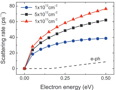
pair states which satisfy energy and momentum conservation in the linear band structure of graphene. β is defined as the angle between the long axis and the line OC andβ′ between the long axis and the line OC′. . . . 24 Figure 2.2 Electron-electron scattering rate for electron concentrations n = 1 ×
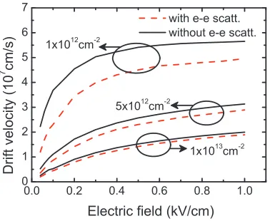
1012cm−2(circle),n= 5×1012cm−2(square), andn= 1×1013cm−2(triangle). The electron-phonon scattering rate is also plotted for comparison (dashed line), [1] where the details at low energies are not discernible due to the linear scale. . . 25 Figure 2.3 Drift velocity for n = 1×1012 cm−2, n = 5×1012 cm−2, and n =
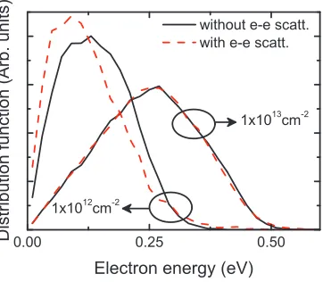
1×1013 cm−2 with (dashed line) and without (solid line) e-e scattering. . 26 Figure 2.4 Energy distribution function forn= 1×1012cm−2andn= 1×1013cm−2
with (dashed line) and without (solid line) e-e scattering. . . 27 Figure 2.5 Calculated Ediff/Etotal (solid line) and vx/vf (dashed line) as a function
of angle β′ assuming that the long axis (x) of the ellipse is along the direction of the electric field.Etotal =E(k′1) +E(k′2) andvf is the Fermi velocity. . . 28 Figure 2.6 Surface polar phonon scattering rate of graphene electron on SiC, SiO2,
and HfO2, for the electron density n of 1×1012 cm−2 at 300 K. Also plotted is the intrinsic graphene optical phonon scattering rate at 300 K (”intrinsic”) obtained from Ref. [1]. . . 29 Figure 2.7 Electron drift velocity in graphene on SiC, SiO2, and HfO2. The intrinsic
case without substrate is also shown. The electron density is 1×1012cm−2 at 300 K. . . 30 Figure 2.8 Electron distribution function with different substrate conditions:
intrin-sic (dash-dotted), SiC (solid), SiO2 (dashed), and HfO2 (dotted), for the ky = 0 cross-section at 20 kV/cm. The box-like function corresponds to the Fermi-Dirac distribution displaced by the SiO2 SPP energy (60 meV) in a simple, metal-like approximation (i.e., EF ≫ kBT) with n = 1×1012 cm−2. For comparison, the equilibrium Fermi-Dirac distribution at 300 K is also plotted. . . 31 Figure 2.9 Electrical resistivity vs. temperature with different substrate conditions:
intrinsic (circle), SiC (square), SiO2 (triangle), and HfO2(diamond), with n= 1×1012 cm−2. The slope of the straight lines are used to extract the acoustic deformation potential. . . 32 Figure 2.10 Drift velocities vs. electric field for graphene on different substrates. The
Figure 2.11 (a) Graphene lattice temperatureTg and (b) temperature differenceTg− Ts between the graphene lattice and the top surface of the substrate as a function of driving electric field. The conditions are the same as in Figure 2.10. . . 34 Figure 2.12 Saturation velocityvsat vs. electron density in graphene on different
sub-strates. In the calculations, it is assumed that the graphene film of 1 µm × 1 µm is under an electric field of 30 kV/cm. The impurity density is 5×1011 cm−2. The experimental data for the case of SiO2 substrate are from Refs. [2] and [3]. . . 35
Figure 3.1 Intrinsic electron scattering rates in MLG and BLG calculated from the first principles for the dominant (a) acoustic and (b) optical phonons. [1, 4] The sudden increases shown in (b) are due to the onset of optical phonon emission. They correspond to the phonon frequencies at the points of high symmetry in the first Brillouin zone: ωΓ≈200 meV and ωK ≈160 meV. . 45 Figure 3.2 Electron-hole propagator Π(q) normalized to N0 (= 2m∗/π~2) in MLG
and BLG with the graphene electron density of 5×1011cm−2. For BLG, the calculation considers different interlayer biases with the induced en-ergy gap Eg of 0 eV (no bias), 0.10 eV, 0.18 eV, and 0.24 eV, respectively. 46 Figure 3.3 Electron drift velocity versus electric field in (a) MLG and (b) BLG,
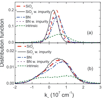
with different substrate conditions: intrinsic/no substrate (circle), SiO2 (triangle), SiO2 with impurities (reverse triangle),h-BN (square), andh -BN with impurities (diamond). The electron density is 5×1011 cm−2 at 300 K. The impurities on the surface of the substrate (d=0.4 nm) have the density 5×1011 cm−2. . . 47 Figure 3.4 Cross sectional view (ky=0) of electron distribution functions in (a) MLG
and (b) BLG at 20 kV/cm, with different substrate conditions: intrin-sic/no substrate (short dashed line), SiO2 (long dashed line), SiO2 with impurities (solid line), h-BN (dashed-dotted line), and h-BN with impu-rities (dotted line). The conditions are the same as specified in Fig. 3.3. . 48 Figure 3.5 Density of states in BLG for different interlayer biases with the induced
energy gap Eg of 0 eV (solid line), 0.10 eV (dashed line), 0.18 eV (dotted line), and 0.24 eV (dashed-dotted line), respectively. The inset shows the corresponding band structures. . . 49 Figure 3.6 Electron mobility versus bias-induced bandgap in BLG at 300 K, with
different substrate conditions. The electron density is 5×1011 cm−2. The impurities on the surface of the substrate (d=0.4 nm) have the density 5×1011 cm−2. . . 50 Figure 3.7 Electron drift velocity versus electric field in BLG with a bias-induced
Figure 4.1 Electronic and phononic band structures of monolayer silicene along the symmetry directions in the FBZ. The Dirac point serves as the reference of energy scale for electrons. . . 71 Figure 4.2 (Color online) Electron-phonon interaction matrix elements |gvk+q,k| (in
units of eV) from the DFPT calculation in silicene forkat the conduction-band minimum K point [i.e., (4π/3a,0)] as a function of phonon wave vector qfor all six modesv. . . 72 Figure 4.3 (Color online) Electron scattering rates in silicene via (a) emission and
(b) absorption of phonons calculated at room temperature. The electron wave vector kis assumed to be along theK-Γ axis. . . 73 Figure 4.4 (Color online) Drift velocity versus electric field in monolayer silicene
obtained from a Monte Carlo simulation at different temperatures: 50 K (square), 100 K (triangle), 200 K (diamond), and 300 K (circle). The results in (a) consider the scattering by ZA phonons, while those in (b) do not. . . 74 Figure 4.5 Electronic and phononic band structures of monolayer MoS2 along the
symmetry directions in the FBZ. The conduction-band minimum at the
K point serves as the reference of energy scale for electrons. . . 75 Figure 4.6 (Color online) (a)-(e) Electron-phonon interaction matrix elements|gvk+q,k|
(in units of eV) from the DFPT calculation in MoS2forkat the conduction-band minimum K point [i.e., (4π/3a,0)] as a function of phonon wave vectorq. Only the branches with significant contribution are plotted; i.e., TA, LA, TO(E′), LO(E′), and A1 (or homopolar) modes. (f) Schematic illustration of intervalleyscattering for electrons in theK valley. . . 76 Figure 4.7 (Color online) (a)-(e) Electron-phonon interaction matrix elements|gvk+q,k|
(in units of eV) from the DFPT calculation in MoS2 forkat theQ point [i.e., Q1 ≈ (2π/3a,0)] as a function of phonon wave vector q. Only the branches with significant contribution are plotted; i.e., TA, LA, TO(E′), LO(E′), and A1 (or homopolar) modes. (f) Schematic illustration of
in-tervalley scattering for electrons in the Q valleys. . . 77 Figure 4.8 (Color online) Scattering rates ofK-valley electrons in MoS2via (a)
emis-sion and (b) absorption of phonons calculated at room temperature. The electron wave vectork is assumed to be along theK-Γ axis. . . 78 Figure 4.9 (Color online) Scattering rates ofQ-valley electrons in MoS2 via (a)
emis-sion and (b) absorption of phonons calculated at room temperature. The
Q-K separation energyEQK (= 70 meV) denotes the onset of curves as theK-valley minimum serves as the reference (zero) of energy scale. The electron wave vectork is assumed to be along theQ-Γ axis. . . 79 Figure 4.10 (Color online) Drift velocity versus electric field in monolayer MoS2
ob-tained from a Monte Carlo simulation at different temperatures with EQK= 70 meV. When electron transfer to theQvalleys is not considered,
Figure 5.1 Principles of electron guiding in TI. The electron wave can propagate along the direction of Dirac cone shifting, while be blocked along the perpendicular direction, as indicated by the green arrows. . . 90 Figure 5.2 Device schematic for waveguiding: (a) blocking the electron wave; (b)
steering the electron wave by 90◦. . . 91 Figure 5.3 The electron wave density from FDTD simulation for electron guided by:
(a) gate voltage; (b) proximity effect with FMI. The electron wave density is normalized by the maximum value. The width of the waveguide is 100nm. 92 Figure 5.4 The electron wave density from FDTD simulation for: (a) blocking the
electron wave; (b) steering the electron wave by 90◦.The electron wave density is normalized by the maximum value. The width of the waveguide is 100nm. . . 93 Figure 5.5 NEGF simulation results for the blocking operation. (a) Calculated
Chapter 1
Introduction
The searching for new materials used in novel semiconductor devices and integrated circuits has been driven by the increasing demand of computing power. Lots of material properties have to be carefully examined for particular applications, such as size of band gap, mobility, saturation velocity, scalability, surface and edge properties and so on. Particularly, two dimensional mate-rials, such as graphene, [5, 6, 7] silicene, [8, 9, 10, 11] transitional metal dichalcogenides, [12, 13] and topological insulators, [14, 15, 16, 17] have attracted huge interests recently, due to their intriguing electrical and optical properties, perfect candidate to explore fundamental physics, and potentials in novel applications.
has the linear dispersion, E = ~vF|k|, while more interestingly, the eigenfunctions have two components corresponding to the two sublattices, which give the quasiparticle the Berry phase of π. [26, 27] This two-component part of the wavefunction is usually referred as pseudospin. Due to the conservation of this quantity, graphene demonstrates many exotic phenomena, such as chiral quantum Hall effect, [28, 29, 30] chiral tunneling and klein paradox, [20, 31, 32], weak localization, [33, 34, 35] and universal conductance fluctuations. [36, 37]
In addition to the tremendous research on the fundamental physics of graphene, the most attracting ability of graphene is its amazing transport properties, which not only endow the value of research but also have the practical significance for electronic and optoelectronic semi-conductor devices. Graphene has shown the ultra-high mobility and large saturation velocity, which allows it to bare six time larger current than Cu. Experimentally, the measured mobil-ity of graphene have the range from 103 ∼ 106 cm2/Vs, [38, 39, 40, 41, 42, 43, 44] while the mobility for Silicon is 1350 cm2/Vs, for GaAs is 4600 cm2/Vs, and for 2DEG in AlGaN/GaN is 1500 ∼ 2000 cm2/Vs. [22] At the same time, the carrier saturation velocity in graphene is over 4×107 cm/s, much higher than that in conventional semiconductor: Silicon∼1×107 cm/s, GaAs ∼2×107 cm/s and InP ∼0.5×107 cm/s. [23] Higher carrier saturation velocity provides the capability for the larger saturation current. Thus, in integrated circuits, the transistor can have smaller width while maintaining the fan-out ability. These properties of graphene are de-termined by the various scattering mechanisms from its own phonons and extrinsic scattering sources. The mobility is strongly dependent on the substrates, due to the charged impurity scat-tering, surface polar phonon scatscat-tering, and other defect scatscat-tering, such as vacancies, ripples and cracks.
the density of states and scattering time around Fermi level. Despite of the usability in logic level, graphene has demonstrate remarkable performance in high speed analog devices. [46, 45, 47, 48, 49, 50] The graphene transistors showed good scalability of the gate length, and the potential performance with higher cut off frequency. But one of the drawbacks is the weak current saturation of the transistor, which is caused by the zero bandgap and conducting of the two type of carriers. [47, 46, 48] The unsaturated current is not favored in RF applications, since it may result to the very small, or even negative, transconductance at high drain-source voltage.
Compared to the monolayer graphene, bilayer graphene, consisting of two layers of carbon films with each having two sublattices, has one apparent advantage that the bandgap can be induced by breaking the inversion symmetry between two layers. [30, 51, 52, 53] One common way is to apply perpendicular electric field, which can achieve a finite band gap of hundreds of meV and form a band structure with a shape of ’Mexican hat’. [51, 54] Another practical route is to dope top layer graphene with adsorption atoms, e.g. potassium, in order to induce the internal electric field to break the symmetry. [55] In particular, a current on/off ratio of 100 can be obtained at room temperature, giving the implication that bilayer graphene may be the better choice for logic device. [56]
photode-tector, the bandwidth is largely improved compared to those materials with bandgaps, since photons with energy lower than the bandgap can penetrate the materials without being ab-sorbed. The ultra high mobility is also an advantage for ultra fast photodetector based on graphene. [64, 65, 66] For example, Ref. [66] reported a maximum external photoresponsivity of 6.1 mA·W−1 can be achieved at a wavelength of 1.55µm, and possible operational wavelength from 300nm to 6µm could be realized in future. Moreover, for on-chip optical communications, graphene can be used as the ultrafast optical modulator due to its tunability of the Fermi level, compactness of footprint, and the broadband of absorbance. [67]
The ideal physical properties of graphene and its derivatives make them the very promising candidates for electrical and optoelectronics devices. Its extreme high mobility gives ultrafast speed to the devices, the nature of chirality of Dirac fermions brings in the possibilities for new type of devices, such as BISFET and pseudospin valve, [68, 69] and the zero bandgap and strong electron-photon interaction can be utilized in optical devices enabling the response for a wide range of frequency. Recently, lots of effort have been spent on producing large area and high quality graphene with low cost, [61, 70, 71] which will speed up the commercialization of graphene based applications in future.
Besides graphene, the attention to other low-dimensional materials has expanded widely. [72, 12, 13, 73] In particular, silicene [8, 9, 10, 11], on type of group IV materials with atomic thick-ness, and molybdenum disulfide [74, 75, 76, 77], one type of transitional metal dichalcogenides (TMDs), have gained much interest due to their unique properties in electronics, optoelectron-ics, and magnetics. Silicene is expected to share certain superior properties of graphene due to its structural similarity and the close position in the periodic table. More importantly, it is compatible with the current silicon-based technology and can be grown on a number of different substrates. [78, 79, 80, 81, 82]
the phonon energy through first principles calculation. [10] Only low-buckled structure for free standing silicene can exist and show positive phonon frequency in the first principles calculation. The electron dispersion shows Dirac cone formed by theπ andπ∗bands, with the Fermi velocity about half of that in graphene. When putting silicene on subtrates, the Si layer is reconstructed to a more complicated triangular structures. Correspondingly, in presence of the substrate, the band structure shows a band gap, which is verified by both ARPES experiment and DFT calculations. [11, 80] The opening of the band gap resembles the case with graphene on substrate. For instance, large band gap about∼0.74 eV is observed for graphene on Ir with Na adsorption as well as band gop of 0.26 eV for graphene on SiC substrate. [83, 84] For silicene on substrate, two factors would induce the opening gap, the interaction between silicene and the substrate, and the atomistic bulking by itself. The DFT calculation in Ref. [80] confirmed that the band gap is induced primarily due to the latter factor. This discover also indicates the potential band structure engineering for epitaxial silicene through strain engineering, such as self-doping and semimetal-metal transition. [85, 86, 87, 88]
Also, the silicene nanoribbon shows very interesting electronic and magnetic properties, strongly depending on the width and orientation. For example, the armchair nanoribbons have oscillatory band gaps with decreasing width. Zigzag nanoribbons exhibit both metallic ferro-magnetic and antiferroferro-magnetic states, whose energy can be different if the edge is passivated by hydrogen. . [10] The magnetoresistance for zigzag silicene nanoribbons is estimated to reach the order of 106%. [89] The mobility based on the deformation potential theory for silicene nanoribbon is preditected to oscillate with the width, which is on the same order of magni-tude of that in graphene nanoribbon. [85] Additionally, the silicene nanoribbon is predicted to be a very promising thermoelectric materials. Recent theoretical study using nonequilibrium Green’s function method and nonequilibrium molecular dynamics simulations predicts that the ZT value for silicene nanoribbon can achieve as high as 4.9 when the doping level is optimized, which is very promising in thermoelectric devices. [90]
ranges from approximately 1.3 to 1.9 eV depending on the thickness. [74] It has been used as the channel material in field effect transistors with promising results, such as channel mobility measured from 200 up to 1000 cm2/Vs, room temperature current on/off ratio up to 108, and subthreshold swing 74 mV/dec. [75, 91] In addition, monolayer MoS2 offers the possibilities of interesting spin and valley physics utilizing the strong spin-orbit coupling. [92, 93, 94, 95] Due to the combination of inversion symmetry breaking and spin-orbital coupling, electrons in the valence band edge can have very long relaxation time for both spin and valley index, since the flipping violates the symmetry. When shining light to monolayer MoS2, only the certain interband transitions can happen depending on the polarization and frequency of the light source. Through this way, Ref. [95] demonstrates a complete valley polarization in monolayer MoS2, with the retention time longer than 1 ns.
Chapter 2
Electrical Transport in Monolayer
Graphene
2.1
Introduction
Accurately modeling and calculating the electrical properties of graphene, such as mobility and saturation velocity, are essential for utilizing this material in practical usage. The mobility and saturation velocity are limited by various conditions, including different source of scattering, temperature, Joule self heating, substrate and so on. In this chapter, we adopt Monte Carlo simulation method to study the electrical transport properties in monolayer graphene. Several scattering source are included in the simulation. Their influence on the transport properties are carefully studied and discussed. As an important issue in modern integrated circuits, Joule self heating effect is very crucial to the electron transport, and strongly depending on the choice of substrate. In section 2.4, we will discuss this effect particularly.
2.2
Electron-electron scattering
inter-carrier collisions deserve careful consideration in the determination of the transport properties. Das Sarmaet al.[117, 118] found the inelastic e-e scattering rate and mean free path in graphene through the analysis of the quasiparticle self-energies. The scattering rate, calculated for electron densities from 1∼10×1012cm−2, was found to be of the same order of magnitude for electron-phonon scattering rates evaluated in the deformation potential approximation. [119] Several authors have considered the electronic transport properties of graphene based on approaches such as the Monte Carlo simulation (see, for example, Ref. [120]); however, the effects of e-e scattering have yet to be addressed. On the other hand, those utilizing the perturbative Green’s function approach accounted for the many-body effect of e-e interactions in graphene but only at very low (zero) temperatures and without electron-phonon relaxation. [121] In the present analysis, we examine the influence of this (e-e) interaction mechanism in intrinsic monolayer graphene at room temperature. A full-band ensemble Monte Carlo method is used for accurate analysis of the distribution function as well as its macroscopic manifestations, particularly, the electron low-field mobilities and drift velocities.
In both bulk and two-dimensional conventional semiconducting systems, e-e scattering has been well studied as is documented in the literature. [122, 123, 124] During an e-e scattering event, both the energy and momentum are conserved. In a parabolic band structure, common in conventional semiconductors, momentum conservation directly leads to the conservation of velocity. This can be readily shown by multiplying the momentum conservation equation by
~/m, which gives v1 +v2 = v′1 +v′2. It is then clear that, in a material with a parabolic
band structure, e-e scattering has no direct effect on the drift velocity (which is an ensemble averaged quantity). The situation becomes different in graphene, where the energy dispersion in the region of the inequivalent Dirac points is linear, therefore removing the constraint that momentum conservation leads directly to velocity conservation.
Fermi’s golden rule
s(k1,k2;k′1,k′2) =
2π
~ |M|2δ[E(k′1) +E(k2′)−E(k1)−E(k2)], (2.1)
where E(k) is the electron energy dispersion relation and k′1 and k′2 are the wavevectors of the final states after scattering. The matrix element of interaction |M|, when accounting for exchange scattering (i.e., the indistinguishability of electron pairs with like spin after collision), is given by [126]
|M|2 = 1 2[|V(q)|
2+|V(q′)|2−V(q)V(q′)], (2.2)
where the Coulomb scattering matrix V(q) between two electrons (k1→k1′;k2 →k′2) is
V(q) = 2πe 2
ϵ(q)qA
1 + cos(θk1k′
1) 2
1 + cos(θk2k′
2)
2 (2.3)
with q = |k1 −k′1|. In the expression, ϵ(q) is the static dielectric function, θkk′ is the angle
between the wavevectorskandk′, andAis the normalization area. The corresponding element V(q′) (k1 → k′2; k2 → k′1) can be expressed likewise with q′ = |k1 −k′2|. The dielectric
function is considered in the random-phase approximation, which is valid for densities n ≥ 1×1012 cm−2. [118] A detailed expression ofϵ(q) used in the study can be found in Eqs. (20)-(22) of Ref. [118]. The scattering rate, including the effect of degeneracy, is then obtained as the double sum over all the final states k′1 and the partner electrons k2 (with k′2 determined
by momentum conservation)
1 τee(k1)
=∑
k2
∑
k′1
s(k1,k2;k′1,k′2)f(k2)[1−f(k′1)][1−f(k′2)], (2.4)
where thef’s are the occupation probabilities.
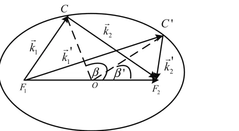
However, by considering the equations of momentum and energy conservation, it can be shown that all the possible final states after scattering lie on an ellipse defined byk1+k2 =k′1+k′2 and
|k1|+|k2|=|k′1|+|k′2|. As shown in Figure 2.1, the initial point (i.e., the coordinate centrum
at theK orK′ point in the Brillouin zone) and the terminal point of the vectork1+k2 specify
the two foci of the ellipse (i.e.,F1 andF2), with the length of long axis of the ellipse determined by |k1|+|k2|.
Our Monte Carlo model applied in the simulation includes the full electronic band structure as calculated in the tight binding approximation. The electron-phonon scattering rates and phonon dispersion relations, previously obtained from a first principles approach based on density functional perturbation theory, are included for all six branches. [1] All electron-phonon transition possibilities, including intravalley and intervalley, are accounted for as well as the e-e scattering. Finally, since our simulations include large electron densities we account for degeneracy, where Pauli exclusion is non-negligible, by implementation of the rejection technique in the selection of the final state after scattering. [128] The non-equilibrium electron distribution function is obtained self-consistently through simulation.
fields coincides with the emergence/prevalence of optical phonon scattering via emission. This suggests that the presence of other competing interaction mechanisms (i.e., substrate dependent surface polar phonons, remote impurities, etc.) may further wash out the e-e induced effect.
To examine the origin of velocity degradation, the electron energy distribution is analyzed in Figure 2.4 at E = 1 kV/cm. Just as in conventional semiconductors, e-e scattering results in an extension of the thermal tail of the distribution function, while simultaneously shifting its peak backward (e.g., see the curves with n = 1×1012 cm−2). This large split in the final state energiesE(k′1) andE(k′2) tends to decrease the average drift velocity in graphene with a linear dispersion. As indicated in Figure 2.5, selection of largeEdiff (=|E(k′1)−E(k′2)|) for the
final electron pair clearly coincides with a small ensemble velocity vx (=v1x′ +v2x′ ) along the direction of the field (i.e., thexaxis) after scattering. At larger densities, the lowest energy states are already mostly occupied, thereby further preventing transition to the energy states (i.e., largeEdiff) which most greatly reduce the drift velocity. In other words, the degeneracy factor in Eq. 2.4 (which was not accounted for in Figure 2.2) significantly reduces these scattering events. Accordingly, the e-e induced effect is largely suppressed for n= 1×1013 cm−2 (see Figures 2.3 and 2.4). Note that the e-e scattering should also approach to zero as the electron density becomes negligible. This means that the predicted degradation may be the most significant at moderate densities (say, ≈ 1011−1012 cm−2). However, n < 1012 cm−2 is beyond the range of this investigation owing to the limitation imposed by the random-phase approximation. A more sophisticated model for screening is needed to further quantify the impact.
2.3
Surface polar phonon dominated transport
When a graphene layer is in close proximity to a polar substrate, inelastic carrier scattering with surface polar phonons (SPPs) can result in significant reduction in the low-field mobility of graphene. [41, 130, 131, 132] Due to the inelastic nature of SPP, they also provide pathway to current saturation, in conjunction with, or as a substitute for, intrinsic optical phonons. While a number of studies generally suggested the negative influence of reduced saturation velocities (due to the relative small energies of SPPs),[2, 133, 134] conflicting reports exist that predict a very different picture (including enhanced velocities) based on the analysis of Boltzmann transport equation. [132, 135]
In this section, we investigate the influence of carrier scattering due to SPPs on the electronic transport properties of monolayer graphene, via a full-band ensemble Monte Carlo method. Par-ticularly, the low-field electron mobility and saturation velocity are calculated in the presence of three different substrates (SiC, SiO2, and HfO2) and compared with those of intrinsic graphene at room temperature. Furthermore, we examine the impact of SPPs on the low temperature electrical resistivity, with attention to its implication on the experimental determination of the acoustic phonon deformation potential constant.
The Monte Carlo model adopted in the calculation utilizes the complete electron and phonon spectra in the first Brillouin zone. While a tight-binding band is used for the electronic energy structure, all six branches of the graphene phonon spectra are considered with the phonon dis-persion and electron-phonon scattering rates obtained fromfirst principles calculations. [1] The effect of degeneracy is accounted for by the rejection technique, after final state selection. [136] The distribution function is obtainedself-consistently from the ensemble simulation. The SPP scattering rate is introduced by following [130, 131]
1 τS(ki)
= 2π
~
∑
q
e2F2 2ε(q)2
e−2qd
q (1 + cosθ)(nq+ 1 2 ±
1
2)δ(Ef −Ei±~ωS), (2.5)
the distance between monolayer graphene and the substrate (0.4 nm), ωS the SPP energy, and F2 = ~ωS
2Aε0( 1 κ∞S+1 −
1 κ0
S+1
) the square of Fr¨ohlich coupling constant. The (1 + cosθ) factor originates from the overlap integral of the pseudospin part of the electron wavefunction and ε(q) is the dielectric function in graphene. In addition, F contains the dependence on high (low) frequency dielectric constant of the polar substrate κ∞S (κ0S) along with the normalized area A. The scattering by ionized impurities in the substrate is not included in the effort to clearly identify the role of SPPs. The values for relevant substrate parameters can be found in Refs. [132, 130, 131].
Figure 2.6 shows the SPP scattering rates calculated at 300 K for three substrates, SiC, SiO2, and HfO2. For comparison, the strength of electron-optical phonon interaction inherent in graphene (via the deformation potential) is also plotted from a first-principles analysis. [1] The results clearly illustrate the dominance of SPPs over intrinsic optical phonons in graphene for the entire electron energy under consideration. Furthermore, this enhancement in scattering is more pronounced for the substrates with small ωS that is apparent from the onset energy of emission process (e.g., HfO2- 19.4 meV; SiO2- 60.0 meV; SiC - 116 meV). Due to the Coulombic nature, the SPP scattering is a function of electron density n and subsequent screening in graphene. Throughout the calculation, we assume n = 1×1012 cm−2 along with the static screening function ε(q) in the random-phase approximation. [118] The intrinsic scattering via deformation potential interaction has no dependence onn.
on the onset of optical phonon emission, intrinsic phonon or otherwise (i.e., SPPs). Rather, it is in general agreement with more recent studies that solved the Boltzmann transport equation numerically assuming a displaced Fermi-Dirac distribution function. [132, 135]
The apparent inconsistency of increased total scattering rate and absence of velocity degra-dation in the high-field region may be explained by considering the linear energy dispersion and the characteristics of the Fr¨ohlich interactions. As it is well known, a change in electron energy (say, via an inelastic scattering) does not automatically relax the drift velocity in monolayer graphene near the K and K′ points. What matters is the direction of the final momentum. Due to the Coulombic nature, the Fr¨ohlich interactions, including those by SPPs, prefer small angle events. When a SPP scattering occurs, the electron will likely emit (absorb) a SPP, with the phonon momentum pointing along the radial direction toward (away from) the Dirac point. Consequently, the velocity of the scattered electron may not change significantly. In contrast, optical phonon scattering of intrinsic graphene is via deformation potential interactions and, thus, randomize/relax effectively the direction of the electron momentum/drift velocity. Ignor-ing the difference between the Fr¨ohlich and deformation potential interactions [133] can lead to inaccurate depiction of transport properties.
very strong inelastic scattering by surface phonons, the drift velocity may not have reached the saturation point at 20 kV/cm and could grow further. Cooling of electron distributions via surface phonon interactions may also reduce the self-heating as the generated heat (i.e., SPPs) is on the substrate and, thus, can be more readily dissipated. Another interesting point to note from Figure 2.8 is that the electron distribution function in graphene does not resemble that of a highly degenerate case, certainly not when subject to an appreciable electric field. A simple approximation of a displaced box-like function [2, 134] cannot describe transport properties accurately.
non-polar substrate (7.8 eV). [138] For the SiC substrate, we estimateDac ≈7.1 eV similar to the intrinsic result. As T &150 K, however, there is a substantial increase in SPP scattering and the difference between the SiC and intrinsic cases becomes more discernible. When SiO2is used as the substrate, the slope of ρ is further increased and becomes nonlinear earlier due to the small SPP energy. The deduced value in the linear region (T .125 K) gives the appearance of Dac ≈13.2 eV, which is not unlike 16−18 eV estimated experimentally on SiO2. [41] Finally, HfO2 has the largest effect among the three substrates. The resistivity is greatly increased with no apparent linear region in the temperature range under consideration. Accordingly, it is not plausible to determine Dac. The relevance of SPP scattering even in the T . 150 K regime can explain, at least in part, the very disparate results for the magnitude of acoustic phonon deformation potential in graphene. [41, 132, 1, 138]
In summary, we investigate the effects of substrate-induced SPP scattering on the electronic transport properties in monolayer graphene by using a full-band ensemble Monte Carlo simu-lation. It is found that the electron velocity-field characteristics are highly dependent on the choice of substrate at room temperature. Specifically, the Fr¨ohlich nature of the interaction appears to be crucial for correctly describing the saturation of drift velocity. The simulation also shows that the SPP scattering remains an efficient mechanism even at low temperatures (T & 50 K), substantially affecting the electrical resistivity. This makes it difficult to experi-mentally determine the acoustic deformation potential for intrinsic graphene in close proximity to a substrate.
2.4
Joule self heating effect
with the lattice is essentially a thermalization process from a system point of view. As electrons gain energy from an external source (such as an electrical bias), a part of the excess energy is transferred to the lattice via phonon emission. Subsequent increase in the lattice temperature (i.e., the Joule heating) acts as a counter weight to limit further energy gain from the source by causing degradation in the electronic transport. Eventually, a balance is reached and the system approaches the steady state. Thus, the details of heat dissipation including the properties of its primary path (i.e., the substrate) could have a major influence. This is even more so in graphene based structures, [139] where the two-dimensional (2D) nature dictates a large interface with the substrate compared to the volume.
In this Letter, we theoretically investigate the effect of Joule heating in graphene. Specifi-cally, the impact of different substrates on graphene electron transport properties are examined with four technologically important candidate materials: SiO2, SiC, hexagonal BN (h-BN), and diamond. While SiO2 is the most commonly used substrate due to its compatibility with conventional technology, [2, 3] SiC has seen its use in producing large-area graphene by solid state graphitization. [140] Recently, h-BN has drawn attention for its structural similarity to graphene − a much desired condition for high quality samples. [141] On the other hand, dia-mond can also be a possibility. Beside the anticipated affinity with graphene, it is one of the most thermally conductive materials. In the analysis, we consider a model problem, where a small graphene sample is placed on a 2D plane of relatively thick dielectric or substrate (300 nm), which is in turn on top of a bulk Si layer. The graphene film is subject to a uniform electric field, generating excess heat that must be dispersed through the layers underneath. To obtain the self-consistent solution across the structure, we solve simultaneously the 3D heat transfer equation (including the estimated interfacial thermal resistance) and the Monte Carlo electron dynamics in graphene.
whereas a tight binding model is used for the electronic energy bands. [19] In addition, graphene electron interactions with charged impurities (5×1011 cm−2) on the substrate surface [142] as well as the surface polar phonons (SPPs) are included. [132] For simplicity, the phonon system is assumed to reach thermal equilibrium fast enough such that the electron-phonon scatter-ing rates, for both intrinsic graphene phonons and SPPs, have the temperature dependence based on the Bose-Einstein distribution: i.e., Nq = 1/[exp(~kωBphT)−1], whereωph is the phonon frequency,kB the Boltzmann constant, and T the temperature (a function of position).
The electron energy transferred to the lattice vibrational modes increases the lattice temper-atures of graphene and the substrate. Specifically, the interaction with graphene phonons (e.g., emission) leads to the elevation of graphene lattice temperature (Tg), whereas the substrate has contributions from both the direct excitation of SPPs (i.e., electron-SPP scattering) and the heat conduction from the graphene lattice. As summarized above, the thermal part of the self-consistent model utilizes a 3D heat transfer equation in the substrate;∇·[κ(x, y, z)∇T(x, y, z)] = 0, where κ is the thermal conductivity of the material. The values used in the calculations are κSiO2 = 1.4 Wm−1K−1,κSiC = 370 Wm−1K−1 and κdia= 1800 Wm−1K−1 for SiO2, SiC, and diamond, respectively. [143, 144] Unlike the first three, the thermal conductivity of h-BN is anisotropic with a large difference in the in-plane and the out-of-plane components due to the layered nature; κh-BN∥ ≈300 Wm−1K−1 and κh-BN⊥ ≈2 Wm−1K−1. [145] The corresponding details on Si can be found in Ref. [146].
lonely atoms in order to form a stable surface. [149] The surface may also be passivated inten-tionally to reduce the interface states. As there is an indication that this could cause a drastic increase in rgs, an additional case of fully hydrogen terminated SiC (SiC-H) is considered with rgs = 7.9×10⁻⁸ Km2W−1 to gauge the impact. [148] In a real situation, the surface is more likely to show partial termination (i.e., somewhere between the cases of SiC and SiC-H).
Then, the total power dissipation per unit area across the interface between graphene and the substrate can be expressed asPt= (Tg−Ts)/rgs+Pspp, whereTs is the lattice temperature of the substrate at the interface andPsppis the power transferred via the direct SPP scattering. AsPt should be equal to the net power loss by graphene electrons in a steady state, both this quantity andPspp can be estimated from the Monte Carlo simulation, providing the necessary boundary condition for the heat transfer equation. Finally, a self-consistent temperature profile (includingTg andTs) is obtained by an iterative process.
on a polar counterpart. [150] Indeed, the calculations show that the average graphene electron energy on the diamond substrate is 0.44 eV at 30 kV/cm, while it is for instance only 0.25 eV on SiO2.
To better examine the observed impact on electron drift velocities, the temperatures in the graphene film (Tg) and at the interface directly below (Ts) are provided in Figure. 2.11 as a function of applied bias. BothTgandTsincrease with the field but their magnitudes vary widely depending on the substrate. Clearly, SiO2shows the extreme case of Joule heating with very high Tg and Ts consistent with Figure 2.10. Due to the poor thermal conductivityκSiO2, the excess heat emitted by graphene electrons cannot be efficiently channeled through the substrate. The resulting increase in temperature induces stronger electron-phonon scattering and subsequently degrades the drift velocity. As for h-BN, the rise in Tg and Ts is far more modest despite the very low out-of-plane thermal conductivity κh-BN⊥, which is in fact almost the same as κSiO2. The discrepancy comes from the in-plane thermal conductivityκh-BN∥ that is about two orders of magnitude larger. Consequently, the transferred heat in h-BN can easily spread in-plane unlike in SiO2, utilizing a much wider thermal channel. Indeed, the 3D iso-thermal profile illustrates a laterally extended distribution near the interface−a sign of efficient heat removal. Two substrates with high thermal conductivities, diamond and SiC (unpassivated; not shown), indicate even smaller deviations from room temperature as expected.
via SPP emission appears to be the main reason for the increased Tg−Ts.
Finally, the effect of Joule heating is examined as a function of electron densitynalong with the available experimental studies in the literature. Since the detailed heat dissipation (thus, the extent of Joule heating) depends on such factors as the exact geometry, etc., that not only vary from sample to sample but also are not fully characterized, it is rather difficult to have a meaningful one-to-one comparison at the quantitative level. For instance, when the lateral dimension of the graphene film is much larger than the thickness of substrate dielectric, [139] heat transfer through the structure could simply be projected to a 1D problem with the out-come potentially much different from that considered in the current calculation. The 3D effect such as the lateral heat spread would be absent and h-BN would behave more like SiO2 with pronounced Joule heating. Moreover, the additional structural details including the location and the dimension of metal contacts could alter the heat dissipation pattern that are not in-cluded in the current model. Consequently, we treat the graphene sample size as an effective parameter that is adjusted to provide a good fit with the experimental data (specifically, those on SiO2). [2, 3]
'
β
β
2 k
1
'
k2
'
k2
F
O
C
'
C
1
F
1 k
Figure 2.1: Schematic representation of the initial (k1,k2) and final (k′1,k′2) electron pair states
Chapter 3
Electron Transport Properties of
Bilayer Graphene
3.1
Introduction
research efforts, a comprehensive understanding of electron transport properties in BLG is still a work in progress.
The purpose of the present chapter is to address this issue theoretically by taking advantage of a first principles analysis and the Monte Carlo simulation. Specifically, the impacts of sub-strate conditions and perpendicular electric fields are examined. The calculation results indicate that graphene in the bilayer form loses much of its advantage over conventional semiconductors in the low-field transport, particularly when the band structure is modified to induce non-zero energy gap. The saturation drift velocity, on the other hand, can remain relatively high. Due to the screening, electrons in BLG appear less susceptible to the interactions with remote Coulomb sources, such as SPPs and impurities on the substrates, compared to the monolayer counterparts. Below, we begin with a brief overview of the models used to estimate the relevant scattering rates.
3.2
Relevant Scattering Mechanisms
The strength of the electron-phonon coupling is estimated from the first principles by using the density functional theory. [1, 4] A comparative analysis reveals several qualitative differences in the intrinsic scattering of MLG and BLG. For one, MLG has six phonon branches with two carbon atoms in a unit cell, whereas these numbers double in BLG. Then, BLG may need to consider both the intraband and interband transitions due to the presence of a close second conduction bandπ∗2 in addition to the lowestπ1∗ states. At the same time, the optical phonons in BLG appear to be a relatively weak source of interaction unlike in MLG. Ultimately, the intrinsic scattering rate in BLG is dominated by the long wave acoustic phonons (intravalley scattering). Figure 3.1 illustrates this general trend; only the dominant branches are shown for clarity of presentation. The nomenclature for the phonon modes can be found in Refs. [4] and [1].
A similar treatment can be extended to BLG. By assuming that the electrons are equally distributed in the two layers of BLG, we can derive the corresponding scattering rate as
1 τS(ki) =
2π
~
∑
q
e2F2 ε(q)2
[
e−2qd+e−2q(d+c) 2q
]
×
(
nq+1 2 ±
1 2
)
|gs,sk ′
i (q)|
2δ(E
f −Ei±~ωS), (3.1)
where q = |kf −ki| is the magnitude of the SPP momentum, Ef (Ei) is the final (initial) electron energy, d is the distance between the first layer and the substrate (0.4 nm), c is the interlayer distance (0.34 nm), ωS is the SPP energy, nq is the phonon occupation number, and ε(q) is the dielectric function. Additionally, F2 = ~ωS
2Aε0( 1 κ∞S+1 −
1 κ0
S+1
) is the square of Fr¨ohlich coupling constant, where κ∞S (κ0S) is the high (low) frequency dielectric constant of the substrate. The term|gs,sk ′(q)|2= 12[1 +ss′cosαkcosαk+q+ss′sinαksinαk+qcos 2θ] comes
from the overlap of the electron wave functions of the initial and final states with the scattering angleθ; [154]sands′ are the band indices whose product is +1 for the intraband (for example, π1∗-π∗1) and −1 for the interband (π∗1-π2∗) transitions. [155] For intrinsic BLG,αk=π/2 for an
arbitraryk. When an interlayer bias ofuis applied, it is modified to satisfy tanαk=~2k2/m∗u,
where m∗ is the effective mass of unbiased (or intrinsic) BLG at the K orK′ point. [154] For MLG,|gs,sk ′(q)|2= 12[1 +ss′cosθ]. The specific values for the relevant substrate parameters can be found in the literature. [130, 131, 132] As for the remote impurity scattering, the charged impurities are assumed to be located on the surface of the substrate, in which case the scattering rate is given by
1 τim(ki)
= 2πni A~
∑
q
[
e2 2ε0κε(q)q
]2[
e−2qd+e−2q(d+c) 2
]
In the random phase approximation, the graphene dielectric function can be expressed as [137, 154] ε(q) = 1 −vqΠ(q) with the bare Coulomb interaction vq = e2/2ε0q and the electron-hole propagator
Π(q) = 2 ∑ s,s′,k
|gs,sk ′(q)|2 f s′
k+q−fks
Eks′+q−Eks . (3.3) Here, fks is the electron distribution function in band s and the factor of 2 takes into account the spin degeneracy. Figure 3.2 shows the numerically obtained propagators for MLG and BLG with the graphene electron density ofn= 5×1011cm−2 at 300 K. In this calculation [i.e., Π(q)], electron occupation in theπ∗2states is ignored for its negligible contribution. Compared to MLG, the screening in BLG appears to be much stronger due mainly to the large density of state at the bottom of the conduction band (π1∗). [137] Additionally, the impact of the interlayer potential on the electron screening in BLG can be substantial and is a strong function of temperature.
3.3
Electron Transport in BLG vs. MLG
A full-band ensemble Monte Carlo calculation is used for evaluating electron transport charac-teristics self-consistently. The model takes into account the complete electron and phonon spec-tra in the first Brillouin zone. Specifically, both the graphene phonon dispersion and its interac-tion with electrons are obtained from the first principles calculations as discussed above, [1, 4] whereas analytical expressions from the tight binding approximation are used for the electronic energy bands in MLG and BLG (with the nearest-neighbor hopping energy γ0 = 3.3 eV and the interlayer hopping energy γ1 = 0.4 eV). [156] The effect of degeneracy in the electronic system is taken into account by the rejection technique, after the final state selection. Electron scattering with the SPPs and remote impurities are also considered in the calculation as de-scribed above whenever necessary. Throughout the calculation, we assume an electron density n= 5×1011 cm−2 and T = 300 K.
BLG (with no interlayer bias). It provides a comparison of all examined cases: namely, intrinsic graphene and graphene on two different substrates, SiO2 and hexagonal BN (h-BN), for which a charged impurity density of ni = 5 ×1011 cm−2 is considered along with the SPPs. As illustrated, intrinsic MLG (i.e., no substrate) shows remarkable transport properties, [136, 150] with the mobility and the saturation velocity as high as 1.0×106cm2/Vs and 4.3×107cm/s. An analogous calculation for BLG gives a substantially lower mobility of 1.2×105 cm2/Vs and the saturation velocity of 1.8×107 cm/s. These results for the intrinsic drift velocity are consistent with the scattering rates in Fig. 3.1; they demonstrate how acoustic and optical phonons affect the charge carriers in MLG and BLG at various electric fields.
The lower mobility in BLG can be readily explained by the larger acoustic phonon scattering rates, as well as the lower electron group velocity near the bottom of the conduction band, where all electrons tend to congregate at low electric fields. To understand the smaller saturation velocity in BLG, on the other hand, it is convenient to examine the distribution function at high electric field plotted in Fig. 3.4. As the electrons gain energy in the applied field, the distribution function shifts in the k-space along the direction of the drift. At the same time, increased scattering with the long-wave acoustic phonons leads to a further broadening of the electron distribution. The result of this interplay between the displacement and the broadening is the saturation of the drift velocity in intrinsic BLG, where the acoustic phonons dominate the scattering (particularly, momentum relaxation). In MLG, however, the velocity curve appears to demonstrate another pattern, which points to the presence of a competing intrinsic scatterer. Indeed, as we discussed earlier, the inelastic scattering via optical phonons is strong unlike in BLG, providing efficient energy relaxation for hot electrons. Consequently, the distribution in MLG is prevented from shifting further towards higher energies, which in turn effectively curtails the momentum relaxing interactions and results in a higher saturation velocity. Unlike in the conventional semiconductors, the loss of electron energy does not bring about the reduced group velocity (i.e., the slope) due to the linear dispersion.
into play. That is, the saturation velocity may be actually enhanced when graphene electrons are subject to the SPP scattering, as it provides another path for hot electron energy relax-ation. Moreover, the SPPs prefer small angle interactions (i.e., small momentum relaxation) due to their Coulombic nature. Figure 3.3 clearly demonstrates this effect. In MLG, the SPP scattering can increase the saturation velocity up to 6.5×107 cm/s if SiO2 orh-BN is used for the substrate material. A similar, positive impact of the substrate on the saturation velocity was also suggested in recent studies. [132, 135, 150] In BLG, the saturation velocity can reach 2.9×107 cm/s, which is about as 1.5 times large as the intrinsic value. Apparently, the en-hancement of drift velocity is still prominent despite the stronger screening in BLG leading to smaller SPP scattering rates. This is due partly to the fact that the competing relaxation mech-anism (i.e., intrinsic optical phonon scattering) is relatively weak in BLG as discussed earlier. Nonetheless, interactions with optical phonons (both intrinsic and SPP) provide the dominant energy relaxation process even in BLG; other mechanisms not included in the current study such as emission of photons [157] are not expected to play a significant role in the field range under consideration.
samples of graphene on h-BN frequently show much higher mobility measurements than those on SiO2. This is because the graphene/h-BN interface tends to be naturally of higher quality due to their structural similarity (for example, no dangling bonds). Consequently, one can expect fewer surface impurities/defects, better stability, and reduced roughness (than graphene on SiO2), leading to superior transport characteristics. [158] However, the interface quality varies from sample to sample, making a meaningful comparison rather difficult as it requires a thorough characterization of each interface. Our calculations, on the other hand, assume an identical impurity concentration on both substrates to elucidate the fundamental impact of this scattering mechanism in a direct one-to-one analysis.
3.4
Transport in BLG with interlayer bias
BLG with an interlayer bias offers the advantage of a tunable bandgap with potential applica-tions to transistors, tunable photo-detectors and lasers. [30, 56] The band structure in this case changes to, [51]
Ek2 = γ 2 1 2 +
u2 4 +~
2v2 Fk2±
√
γ14 4 +~
2v2
Fk2(γ12+u2), (3.4)
whereuis the difference between on-site energies in the two layers,vF = ( √
order of magnitude smaller than in the unbiased case. The reduction in the mobility becomes even more pronounced when the ionized impurity scattering is taken into account. The Van Hove singularity also enhances the impact of electron coupling with the remote impurities.
On the other hand, it appears that the velocities at high fields are mostly unaffected by the gap. Figure 3.7 shows the drift velocity foru= 0.1 V, 0.2 V, and 0.3 V, which correspond to the bandgap of 0.1 eV, 0.18 eV, and 0.24 eV, respectively. As the phenomenon of velocity saturation is associated with hot electrons, it is relatively immune from the changes at the bottom of the energy dispersion. Similarly, the impact of the SPP scattering on the drift velocity, as it is felt primarily via the high energy electrons, is not affected by the gap in the electron energy spectrum. Accordingly, no appreciable difference is observed in the saturation velocities for the three considered values of u. When the ionized impurity scattering is included, the velocity saturation is progressively pushed to a higher field due to the reduction in the mobility (i.e., the slope) that was discussed above.
Finally, it may be worth pointing out that the electron-electron scattering could potentially be significant for accurate calculation of low-field transport properties in biased BLG. Due to the diverging density of states at the band minima, electrons tend to congregate in the low-energy states with small momentum vectors, causing stronger inter-carrier interactions. Accordingly, it could limit the accuracy of the obtained mobility values even at the assumed relatively low density of 5×1011 cm−3. This is not a concern in MLG or BLG without the interlayer bias as their density of states is finite even at zero energy.
3.5
Summary
Figure 3.4: Cross sectional view (ky=0) of electron distribution functions in (a) MLG and (b) BLG at 20 kV/cm, with different substrate conditions: intrinsic/no substrate (short dashed line), SiO2 (long dashed line), SiO2 with impurities (solid line),h-BN (dashed-dotted line), and
Figure 3.7: Electron drift velocity versus electric field in BLG with a bias-induced gap of Eg of (a) 0.1 eV, (b) 0.18 eV, and (c) 0.24 eV, under different substrate conditions: intrinsic/no substrate (circle), SiO2 (triangle), SiO2 with impurities (reverse triangle), h-BN (square), and
Chapter 4
Intrinsic Electrical Transport
Properties of Monolayer Silicene and
MoS
2
from First Principles
4.1
Introduction
Characterization of electronic transport, particularly the intrinsic properties, is critical for assessing and understanding the potential significance of a material. In the case of silicene, many of the crucial parameters are presently unknown due to the brief history of this mate-rial. In comparison, notable advances have been made in MoS2 lately. Experimental investiga-tion of transistor characteristics claimed the channel mobilities ranging from ∼200 cm2/Vs to ∼1000 cm2/Vs at room temperature, [75, 91] while a theoretical study estimated an intrinsic