i ABSTRACT
ZDANOWICZ, ERIK MARK. Nanocoining Sub-Micron Features. (Under the direction of Dr. Thomas A Dow.)
The purpose of this research was to develop a new process for creating large arrays of nanofeatures in an economically feasible time frame. Nanostructured surfaces have applications in anti-reflection, surface wetting, pool boiling and Raman scattering applications but currently have no method of mass production. The technique developed, titled ‘nanocoining’ uses a diamond die with a nanostructured area (on the order of 20x20µm) to physically transfer features (~1600 features in nanostructured area) to a mold surface. The challenges that arise from this method are avoiding nanofeature distortion (dragging the nanofeatures on the work-piece surface), precisely indexing indents with respect to other indents and aligning the die with respect to mold surface plane.
The development of the nanocoining process began by investigating indents created using a standard hardness tester and comparing the results to an ANSYS finite element analysis (FEA) simulation. Diamond dies were machined by Focused Ion Beam (FIB) to create slow speed indentations (<1Hz) using the axes of a Diamond Turning Machine (DTM). The process frequency (indents per second) was increased to 1 Hz using a linear Fast Tool Servo (FTS) mounted to the DTM. The Ultramill elliptical actuator previously used for vibration assisted machining (VAM) was retrofit with a diamond die and used for the 1 kHz (1000 indents per second) indentation experiments. The increase in frequency was accompanied by distortion which was defined as relative motion between the nanofeatures on the die and the mold surface. To eliminate distortion, an elliptical tool-path was defined to match the velocity of the die with the velocity of the mold surface at contact.
accomplished using a fixture designed to rotate the die with respect to the mold. Depth of the indents was also a factor which if not properly accounted for led to unwanted diffraction on the indented area.
After refinement, the nanocoining process was demonstrated by creating larger areas of indents in metals including electroless (EL) nickel, hard plated copper, 6061 aluminum and cartridge brass. Differing amounts of pile-up (deformed material pushed above the nominal work-piece surface) were observed for these metals which were found to be a function of strain hardening. Indents were also created on brittle materials including germanium and silicon without fracture due to interesting material effects when subject to high hydrostatic pressure.
i
Nanocoining Sub-Micron Features
by
Erik Mark Zdanowicz
A dissertation submitted to the Graduate Faculty of North Carolina State University
in partial fulfillment of the requirements for the Degree of
Doctor of Philosophy
Mechanical Engineering 2013
APPROVED BY:
_____________________________ _____________________________ Dr. Jeffrey W. Eischen Dr. Mohammed A. Zikry
_____________________________ _____________________________ Dr. Thomas A. Dow Dr. Ronald O. Scattergood
ii BIOGRAPHY
iii
ACKNOWLEDGMENTS
I would like to acknowledge the following people for their assistance during the pursuit of my doctoral degree:
I would like to thank Dr. Thomas Dow for his guidance and mentorship during my entire graduate career. His expertise in precision engineering and mechanical design contributed immensely to my education.
I would like to thank my committee members Dr. Ronald Scattergood, Dr. Jeffrey Eischen and Dr. Mohammed Zikry for their support and guidance during my research.
Ken Garrard and Alex Sohn for providing essential assistance to my work.
John Nowak, Guillaume Robichaude, Brandon Lane and Zack Marston for providing the best assistance they could but more importantly providing opportunities to enjoy occasional adult beverages.
I would like to thank Chuck Mooney of the NCSU Analytical Instrumentation Facility for his expertise, training and all around friendly attitude.
Jim Nelson, Viv Jones and Qunyi Chen from 3M Corporation provided professional guidance in support of my research.
Dr. Khaled Youssef of the NCSU Department of Materials Science for his micro-Raman analysis.
iv
TABLE OF CONTENTS
LIST OF FIGURES ... ix
LIST OF TABLES ... xxii
NOMENCLATURE ... xxiii
1 INTRODUCTION... 1
1.1 Background ... 1
1.2 Anti-Reflective Coatings ... 1
1.2.1 Thin Film Anti-Reflective Coatings ... 2
1.2.2 Anti-Reflective Nanostructured Surfaces ... 4
1.3 Superhydrophobic Surfaces... 8
1.4 Multifunctional Surfaces ... 13
1.5 Surface Enhanced Raman Scattering (SERS) ... 15
1.6 Enhanced Heat Transfer Coefficient in Pool Boiling... 18
1.7 Current Production Techniques ... 22
1.8 Nanocoining Definition ... 25
1.9 Problem Statement ... 26
2 INDENTATION BACKGROUND... 28
2.1 Hardness Testing ... 30
2.1.1 Hardness Test Theory ... 31
2.1.2 Effect of the Indentation Load ... 33
2.1.3 Crack Patterns Formed in Brittle Materials ... 37
2.1.4 Fracture Toughness in Brittle Materials ... 39
2.1.5 Summary ... 39
2.2 Rockwell Indentation ... 40
2.2.1 Rockwell Indenter Experiments ... 40
2.2.2 Finite Element Analysis Modeling of Rockwell Indentation ... 43
2.3 Summary ... 52
3 SLOW SPEED INDENTATION ... 53
3.1 Slow Speed Experimental Setup ... 53
3.1.1 Nanoform 600 DTM ... 53
v
3.1.3 Work-Piece Mounting and Alignment Fixture ... 59
3.1.4 Experimental Setup ... 62
3.1.5 Data Acquisition of Manual Indentation... 64
3.1.6 Manual Indenting with Flat Die ... 65
3.2 Programmed Indentation Experiments with Flat Die ... 68
3.2.1 Nanoform Motion Program... 68
3.2.2 10 x 10 Programmed Array of Flat Indents ... 72
3.3 Programmed Arrays of Nanostructured Indents... 74
3.4 Modeling of Nanostructured Indentations... 77
3.4.1 FEA of Single Nanostructured Indents ... 78
3.4.2 FEA of Multiple Indents ... 82
3.5 Summary ... 89
4 MID SPEED INDENTATION ... 90
4.1 Mid Speed Experimental Setup ... 90
4.1.1 Modified Nanostructured Indenter ... 90
4.1.2 Fast Tool Servo Description ... 92
4.1.3 dSpace Data Acquisition and Controller ... 95
4.2 Mid Speed Indentation Procedure ... 95
4.3 Flat Mid-Speed Indentation Results ... 97
4.3.1 Initial Mid-Speed Indentation Results ... 97
4.3.2 Force Feedback Controller ... 100
4.4 Nanostructured Mid-Speed Indentation Results ... 103
4.5 Summary ... 107
5 FAST TOOL SERVO HIGH SPEED INDENTATION ... 108
5.1 Experimental Setup ... 109
5.2 Indent Procedure ... 110
5.2.1 Diamond Turning the Flat ... 110
5.2.2 Indentation Procedure ... 112
5.3 Results ... 113
5.3.1 Numerical Estimation of Distortion Distance ... 117
5.4 Summary ... 120
vi
6.1 Elliptical Tool Path... 122
6.2 Ultramill Elliptical Actuator... 125
6.2.1 Ultramill Elliptical Tool Path Generation ... 126
6.2.2 Single Channel Light Probe Measurements ... 128
6.2.3 Dual Channel Light Probe Measurements ... 131
6.2.4 Ultramill Tool-Path Shape Prediction ... 134
6.3 Summary ... 138
7 ULTRAMILL HIGH SPEED INDENTATION DEVELOPMENT ... 140
7.1 High Speed Experimental Setup and Procedure ... 140
7.1.1 Indenting Process Parameters ... 142
7.1.2 Centering Procedure... 144
7.1.3 Depth Calibration Procedure... 146
7.2 Material Pick-Up Issue ... 147
7.2.1 Material Influence on Pick-Up... 149
7.2.2 Nanofeature Geometry Effect on Pick-Up ... 152
7.3 Die Alignment and Indent Depth ... 154
7.3.1 Alignment Fixture ... 155
7.3.2 Importance of Indent Depth Control ... 159
7.3.3 Alignment and Depth Calibration Experiment ... 160
7.4 Spindle Speed Considerations ... 164
7.5 Contact Error During Nanocoining of Large Areas ... 168
7.5.1 Ultramill Piezo Temperature Effects ... 169
7.6 Large Area of Indents ... 177
7.7 Source of Diffraction on Indented Part ... 183
7.8 Summary ... 189
8 ANTI-REFLECTIVE INDENTATION... 191
8.1 Anti-Reflective die ... 191
8.2 Initial Indents with AR Die ... 192
8.2.1 Effects of Out-of-Plane Tool-Path Motion ... 194
8.2.2 Ultramill Out of Plane Motion ... 196
8.2.3 Source and Solution to Ultramill Out of Plane Motion ... 199
vii
8.3.1 AR Die Feature Fidelity ... 205
8.4 Summary ... 208
9 NANOCOINING ON GERMANIUM AND SILICON ... 209
9.1 Background ... 209
9.2 Germanium and Silicon Material Behavior ... 209
9.3 Experimental Setup ... 211
9.3.1 Dynamic Indenting Setup ... 212
9.3.2 Static Indenting Setup ... 212
9.4 Results ... 214
9.4.1 Dynamic Indentation Results ... 214
9.4.2 Static Indentation Force ... 217
9.4.3 Nanofeature Deformation Comparison between Ge and Si ... 219
9.4.4 Identification of Phase Transformation ... 220
9.4.5 Crack Formation on Germanium ... 222
9.5 Summary ... 223
10 INDENTATION MATERIAL BEHAVIOR ... 225
10.1 Static Indentations ... 225
10.1.1 Experimental Setup ... 225
10.1.2 Procedure ... 227
10.1.3 Results ... 228
10.2 Section View of Nanostructured Indents ... 229
10.2.1 Fabrication of Work-Piece for Section Indents ... 230
10.2.2 Results of Section Indentation ... 234
10.3 Pile-up and Sink-In Behavior During Nanocoining ... 237
10.3.1 Background on Pile-Up and Sink-In During Hardness Test ... 238
10.3.2 Comparison of Pile-Up on Different Materials ... 242
10.3.3 FEA Investigation of Pile-Up ... 248
10.4 Summary ... 252
11 CONCLUSIONS AND RECOMMENDATIONS FOR FUTURE WORK ... 254
11.1 Summary of Research ... 254
11.2 Highlights of Research ... 257
viii
REFERENCES ... 262
APPENDIX ... 272
APPENDIX A. MATLAB Programs ... 273
APPENDIX B. Fast Tool Servo Simulink Block Diagrams ... 274
APPENDIX C. Cleaning Pick-Up off of Diamond Die ... 276
APPENDIX D. Spindle Speed Induced Error on Nanoform DTM ... 280
APPENDIX E. Heat Transfer Fluid Properties... 286
APPENDIX F. Diamond Die Removal and Attachment ... 287
APPENDIX G. Nanocoining Procedure ... 293
APPENDIX H. G-Code for Nanoform Operations... 305
APPENDIX I. FEA Code for Nanocoining Simulation... 307
APPENDIX J. ASG Spindle Speed Controller ... 311
ix
LIST OF FIGURES
Figure 1-1. Destructive interference from ¼ wavelength film AR coating. ... 3 Figure 1-2. Nano-Feature Array of Peacock Butterfly SEM image [7]. ... 5 Figure 1-3. Cross section of optical layer dissected into thin sub-layers for analysis [9]. ... 6 Figure 1-4. reflective property for different feature height and period. (a) reflective property over full spectrum and varying period with 400 nm height. (b) Anti-reflective property varying height and spacing for 1000 nm wavelength [12]. ... 7 Figure 1-5. Description of contact angle for droplet showing (a) normal (b)
superhydrophobic and (c) superhydrophilic behavior. ... 9 Figure 1-6. SEM image of hierarchal structure of lotus leaf showing (a) multiple micron-scale features (b) single micron-micron-scale feature and (c) nanometer-micron-scale hairs [21]. ... 10 Figure 1-7. Effects of surface roughness on liquid droplet. (a) Liquid droplet on flat surface
(Young’s model) (b) wetted contact on rough surface (Wenzel) (c) hydrophobic contact on rough surface (Cassie) and (d) intermediate between Cassie and Wenzel [20]. ... 11 Figure 1-8. Lotus leaf nanostructures created by (a) Bhushan [22] (b) Sun [23] (c) Liu [24]
(d) and Pozzato [25]. ... 13 Figure 1-9. Multifunctional features created by Min [19]. (a) A 4 in. silicon wafer with one
half covered with features (b) features after 10 min of etch (c) features after 50 min etch and (d) feature depth vs. etch time. ... 14 Figure 1-10. Disk-coupled structures for SERS. (a) Schematic; (b) top-view SEM image; (c)
cross-section SEM image. Figure reproduced from others research [37]. ... 17 Figure 1-11. Diagram of simplified pool boiling experimental setup. ... 18 Figure 1-12. Typical boiling curve for water at 1 atm [44]. ... 20 Figure 1-13. (a) HTC vs. heat flux for surfaces with varying degrees of nanostructures and a
x
Figure 1-15. Nanofeatures created using laser interference lithography. Scale bars are 200 nm [11]. ... 24 Figure 1-16. Nanocoining process where an indenter (a) is pressed into a work-piece causing
material flow (b) until the mold is full (c). The indenter is then removed leaving plastically deformed shape (d). ... 25 Figure 2-1. Typical stress-strain curve for engineering materials. ... 28 Figure 2-2. (a) Stress-strain curve and (b) force-depth curve during indentation process. ... 29 Figure 2-3. (a) Plastic flow pattern proposed by Prandtl, also known as slip-line field theory
[47]. (b) Upward flow of material displaced by indenter in slip-line theory [49]. ... 31 Figure 2-4. Images of a Brinell hardness test on clay (a) and low-carbon steel (b) showing
zone of plastic deformation [47]. ... 32 Figure 2-5. Plastic zone development in Brinell hardness test. (a) Fully elastic (b) elastic-plastic (c) fully developed elastic-plastic zone [49]. ... 34 Figure 2-6. Hardness vs. load for a constant material for (a) diamond pyramid (Vickers)
indenters and (b) spherical indenters (Meyer) [48]. ... 35 Figure 2-7. Contact angle θ for spherical contact with a half-space [49]. ... 36 Figure 2-8. (a) Top view and (b) cross-section view of Vickers indent on a brittle material
[49]. ... 38 Figure 2-9. Spherical indentation crack pattern on a brittle material [52]. ... 38 Figure 2-10. Image of Rockwell hardness tester used for comparison in spherical indentation
modeling. Radius of tip is 200 µm. ... 41 Figure 2-11. Image of hardness tester used to create spherical indents. ... 41 Figure 2-12. Zygo SWLI measurements of Rockwell indents created with (a) 0.2 kg and (b)
0.4 kg on 6061 aluminum. ... 43 Figure 2-13. Initial 2-D model for investigating the behavior of contacting bodies. ... 44 Figure 2-14. Frank-Read source of dislocations. (a) Dislocation pinned by lattice defects.
xi
Figure 2-16. Stress distribution for circular indenter on a flat work-piece. ... 48
Figure 2-17. Displacement vector sum of initial contacting bodies model showing plastic deformation. ... 48
Figure 2-18. FEA setup for Rockwell indentation simulations. (a) Side view showing portion of indenter tip modeled. (b) Angled view showing 3 dimensions and 1/8th model geometry. (c) Contact and target elements on surface of indenter and work-piece with surface normals. ... 49
Figure 2-19. FEA results showing 1.38 µm of deformation for a 0.2 kg load during Rockwell indentation simulation of 6061 Al. ... 50
Figure 2-20. Force-depth curves for FEA simulations of Rockwell indentation on 6061 Al.52 Figure 3-1. Slow speed experimental setup on Nanoform. ... 54
Figure 3-2. Description of the motion of the Nanoform axes. ... 54
Figure 3-3. Geometry of flat indenter provided by 3M. ... 56
Figure 3-4. Zygo SWLI measurement of flat indenter face. ... 57
Figure 3-5. Dimensions of NS indenter face and nano-features. ... 58
Figure 3-6. Border used for alignment on the first nanostructured indenter. ... 59
Figure 3-7. Definition of tilt angle between work-piece and indenter. ... 60
Figure 3-8. Work-piece mounted on Nanoform for slow speed indentation experiments. .... 61
Figure 3-9. Alignment fixture used to correct for tilt angles during slow speed indenting. .. 62
Figure 3-10. Load cell calibration performed on the Nanoform. A known force is applied and resulting voltage is recorded. ... 63
Figure 3-11. Measurment of work-piece tilt angles, θxz and θyz, using the axes of the Nanoform and a LVDT. ... 64
Figure 3-12. Recorded forces for the first set of indentation experiments using the flat indenter on hard plated copper. ... 66
Figure 3-13. Depth measurements from 2nd indentation experiment. ... 67
Figure 3-14. Force vs. depth curve for flat indenter on plated copper work-piece. ... 68
Figure 3-15. Top view of work-piece showing variation in depth due to work-piece tilt. .... 69
xii
Figure 3-17. Slow speed indentation motion program path. Indenter moves across part in x-direction then moves to next row in y-x-direction where process is repeated to create array. 72 Figure 3-18. New View SWLI image of 10 x 10 array of flat indents on hard plated copper.
Right side shows higher magnification. ... 73 Figure 3-19. Sample of forces from 10 x 10 array of flat indents. ... 74 Figure 3-20. New View SWLI image of 11 x 10 array of nanostructured indents on hard
plated copper. ... 75 Figure 3-21. Single nanostructured indent measured with SEM at 5000x (left) and 10000x
(right). ... 76 Figure 3-22. AFM measurement of nanostructure features (left) and 3-D rendering (right). 77 Figure 3-23. Analytical stress distribution solution for flat punch on half-space [55]. ... 78 Figure 3-24. FEA simulation of nanostructured die indent (left) and experimental indent
(right). ... 80 Figure 3-25. FEA displacement of multiple radii die (left), comparison of contact stress
(right). ... 81 Figure 3-26. Simulation of two consecutive indents with flat die. ... 82 Figure 3-27. ANSYS simulation of consecutive indents progress from (a) first indent (b)
initiation of second indent (c) maximum depth of second indent (d) removal of die from second indent and final deformation. ... 83 Figure 3-28. 3D simulation of multiple indents and displacement vector field of single
indent. ... 85 Figure 3-29. Images of deformation caused by each indent from the 3D multiple indent
simulation. ... 86 Figure 3-30. Displacement of the top surface of the work-piece after 3D multiple indent
xiii
Figure 4-3. Alignment device for indenting with FTS. ... 93 Figure 4-4. FTS mounted to the Y-axis of the Nanoform 600. Motion of tool is in z-axis
direction. ... 94 Figure 4-5. Difference in coordinates programmed into the Nanoform between slow and
mid-speed indenting. ... 96 Figure 4-6. 10x10 block of flat indents (1x1 mm) created with FTS on hard plated copper at
1 Hz. (a) Entire array and (b) magnified section. ... 98 Figure 4-7. 10x10 array of flat indents (1x1 mm) created using FTS on hard plated copper at
2 Hz. (a) Entire array and (b) magnified section. ... 99 Figure 4-8. Variation in force along indentation rows using the FTS. ... 100 Figure 4-9. Control diagram for FTS including the force feedback section (shown shaded). ... 101 Figure 4-10. Explanation of threshold in force feedback section of FTS controller. ... 101 Figure 4-11. Image of 2x2 mm (a) and 5x5 mm (b) block created with FTS and force
feedback controller on hard plated copper at 2 Hz. ... 102 Figure 4-12. 1x1 mm block of nanostructured indents created on hard plated copper with
FTS at 2 Hz. Diffraction causes green (a) and purple (b) reflection based on light source incident angle. ... 103 Figure 4-13. Image of intersection of two indents (a) and one indent (b) in the 1x1 mm
nanostructured array. ... 104 Figure 4-14. SEM image of many indents with partial replication (a) and single indent with
partial replication (b). ... 105 Figure 4-15. SEM measurement of diamond NS indenter after 1x1mm array created in hard
xiv
Figure 5-4. (a) SEM image of single indent from third ring and (b) higher magnified view of nanofeatures. ... 115 Figure 5-5. (a) Nanostructured die before FTS indents and (b) after indents. ... 116 Figure 5-6. Material redeposit (outlined) onto work-piece surface. ... 117 Figure 5-7. Plot of vertical die position and work-piece surface position vs. time for one
indent cycle. ... 119 Figure 6-1. Illustration of distortion caused by linear tool-path and moving work-pieice. . 121 Figure 6-2. Elliptical tool path definition at various points in indent cycle. ... 122 Figure 6-3. Plot of expected distortion vs. vertical b dimension of elliptical tool-path. .... 125 Figure 6-4. (a) Image of the Ultramill elliptical actuator and (b) primary components. ... 125 Figure 6-5. Ultramill construction (left) and elliptical motion (right) for EVAM. ... 127 Figure 6-6. Measurement of b dimension of Ultramill ellipse (left) and a dimension (right)
using a single channel light probe. ... 128 Figure 6-7. SEM images showing nanofeatures distorted with Ultramill operating at 1 KHz,
100 V and 7° phase (left) and 13° phase. ... 129 Figure 6-8. SEM images of indents created with phase angle of (a) 15° (b) 20° (c) 25° (d)
30° (e) 35° (f) 40°. ... 130 Figure 6-9. Description of how phase angle will change a dimension of ellipse. ... 131 Figure 6-10. Image of setup to measure Ultramill ellipse using MTI dual channel light
probes. ... 132 Figure 6-11. Ellipse shapes for various phase angles (legends) and amplitude of (a) 50 V (b)
75 V (c) 100 V. Ellipse used in nanocoining experiments (d) has 100 V amplitude and 23.5° phase angle. ... 133 Figure 6-12. Diagram used to develop kinematic model for the Ultramill tool-holder motion. ... 135 Figure 6-13. Measured displacement vs. voltage for Ultramill PZT stacks. ... 136 Figure 6-14. Comparison of simulated Ultramill tool-path ellipse vs. measurement. ... 138 Figure 7-1. Experimental setup for high speed indenting using the Ultramill actuator and
xv
Figure 7-2. Diagram showing Ultramill motion with respect to the Nanoform’s axes. ... 141
Figure 7-3. Orientation of Ultramill ellipse with respect to work-piece rotation. ... 142
Figure 7-4. Indents created with non-centered indenter. ... 144
Figure 7-5. Two-circle method for centering the indenter. ... 145
Figure 7-6. Depth calibration process after centering procedure. ... 147
Figure 7-7. Multiple indents showing material pick-up between die and hard plated copper work-piece at (a) 700x and (b) 3000x. ... 148
Figure 7-8. (a) Diamond indenter with hard plated copper material lodged in-between nanofeatures and (b) the indented work-piece. ... 149
Figure 7-9. Images of indents created on unknown nickel sample with minimal pick-up. . 150
Figure 7-10. Indents on EL nickel sample from Techmetals with no pick-up at (a) 2000x and (b) 20000x. ... 152
Figure 7-11. Shapes of nanofeatures used during indentation experiments. ... 152
Figure 7-12. SEM image of nanofeatures identical to those on the second NS die. ... 153
Figure 7-13. Images of indents created with second NS die on 3M plated copper at (a) 3000x and (b) 37000x. ... 154
Figure 7-14. Tilt angle definition. ... 155
Figure 7-15. Model of indenter with respect to mold (a). Illustration of indenter misaligned in θYZ direction (b), θXZ direction (c) and θXY direction (d). ... 156
Figure 7-16. Alignment fixture designed to rotate indenter in θxz and θyz directions. ... 157
Figure 7-17. Pitch adjustment on the Ultramill alignment fixture. ... 158
Figure 7-18. Yaw adjustment for Ultramill on alignment fixture. ... 159
Figure 7-19. Schematic showing (a) indenter with border and work-piece and (b) SEM of border marks around each indent created when indenter is ‘bottomed out.’ ... 160
Figure 7-20. Ultramill being aligned with the axes of the Nanform using an LVDT gage. 161 Figure 7-21. First indents created with alignment fixture. SEM shows good alignment about the θxz axis and poor alignment about the θyz axis. ... 162
xvi
Figure 7-23. Indents created with indenter aligned parallel to work-piece at (a) 2000x and (b) 500x. Indents also created at appropriate depth. ... 163 Figure 7-24. SEM measurement of indents created using proper alignment, depth control and
centering procedure at (a) 1500x and (b) 7000x. ... 164 Figure 7-25. SEM showing how dissimilarity between indents in successive rings during 200
µm wide large area indenting. ... 165 Figure 7-26. Plot of commanded and actual spindle speed during velocity changes recorded
by spindle encoder. ... 166 Figure 7-27. Plot of spindle speed during a sub-rpm velocity change... 167 Figure 7-28. Large area of indents with un-indented rings on EL nickel. ... 168 Figure 7-29. Experimental setup showing light probe for measuring displacement and a
thermocouple for measuring temperature. ... 170 Figure 7-30. Temperature and mean displacement of Ultramill vs. time for a coolant flow
rate of 0.8 L/min. ... 171 Figure 7-31. Temperature and mean displacement of Ultramill vs. time for a coolant flow
rate of 0.4 L/min then changed to 1.0 L/min at 34 min. ... 172 Figure 7-32. Observation of thermal expansion error in large area of indents. ... 173 Figure 7-33. Temperature and mean displacement of Ultramill vs. time for a coolant flow
rate of 1.0 L/min. ... 174 Figure 7-34. Oscillation of Ultramill PZT temperature during manual tuning of ThermoCube
PID gains. ... 176 Figure 7-35. Temperature and mean displacement of Ultramill vs. time using new gains and
flow rate of 0.8 L/min. ... 177 Figure 7-36. Photograph of nanocoined EL nickel sample... 179 Figure 7-37. SEM images of EL nickel part in Figure 7-36a at (a) 10000x and (b) 2500x. 179 Figure 7-38. SEM of replication created from part shown in Figure 7-36a at (a) high
magnification and (b) reduced magnification. ... 180 Figure 7-39. AFM measurement of back side of replicate. This is what the nickel surface
xvii
Figure 7-40. AFM measurement of the front side of the replicate (bumps) with trace. ... 181 Figure 7-41. 3D view of front of replicate measured by an AFM. Bumps on the surface are
molds of the nanofeatures. ... 182 Figure 7-42. Profile view of plastic replicate at (a) 75000x and (b) 25000x. ... 183 Figure 7-43. Double-slit diffraction of a single wavelength of light. ... 184 Figure 7-44. Determining θ1 from the spacing between the zero and first order diffracted
beams. ... 186 Figure 7-45. Microscope images of indent calibration rings. ... 188 Figure 8-1. AR die showing 250 nm tall features with 250 nm spacing. ... 191 Figure 8-2. Tilt of diamond indenter on ceramic tool holder with respect to the Nanoform
axes. ... 192 Figure 8-3. (a) SEM image showing several initial indents created with AR die and (b)
45000x magnification on the nanofeatures for distortion observation. ... 193 Figure 8-4. Orientation of die, tool holder and ellipse with respect to mold and Nanoform
axes. ... 195 Figure 8-5. (a) Die with some angular mis-alignment on holder and (b) tilting of tool holder
to compensate. ... 195 Figure 8-6. SEM images (a) of several indents and (b) individual nanofeatures after die re-attachment. ... 196 Figure 8-7. Image of (a) one single static indent on Optakoat nickel and (b) individual
nanofeatures. ... 197 Figure 8-8. Measuring the out-of-plane motion of the Ultramill with dual channel light
probes. ... 198 Figure 8-9. Measurement of out of plane motion. ... 198 Figure 8-10. Description of how PZT stacks reside in the Ultramill coolant chamber. ... 199 Figure 8-11. SEM images of indents on 3M hard plated copper after Ultramill reconstruction
at (a) 2000x and (b) 50000x. ... 200 Figure 8-12. SEM images of indents on electroless nickel after Ultramill reconstruction at
xviii
Figure 8-13. Section of indents with complete transfer of features on electroless nickel after Ultramill reconstruction at (a) 2500x and (b) 40000x. Waviness of image is caused by magnetic field in SEM, not a feature of the part. ... 202 Figure 8-14. SEM images showing (a) zero distortion of nanofeatures and (b) indents
indexed precisely. Waviness of image is caused by magnetic field in SEM, not a feature of the part. ... 203 Figure 8-15. SEM image of AR indenter (a) after nanocoining experiments and (b) after acid
etching. ... 204 Figure 8-16. SEM image of AR indenter with magnified regions of nanofeatures. ... 206 Figure 8-17. SEM image of (a) 10x10 µm AR test array with magnified section and (b)
magnified section of 500 nm pitch features. ... 207 Figure 9-1. TEM of (a) a 60 mN indent in Si where material marked ‘t’ has transformed with
some of transformed material flow into the crack marked with the arrow. (b) a 50 mN indent in Ge showing transformed region marked ‘t’ [60]. ... 210 Figure 9-2. Indents created in Si using a constant 80 mN force and constant load rate. (a)
35.3° (corner cube indenter) (b) 45.0° (c) 55.0° (d) 65.3° (Berkovich indenter) (e) 75.0°. [63] ... 211 Figure 9-3. Experimental setup for static indents. ... 213 Figure 9-4. Image showing the Ge and Si sample and diffraction from the dynamically
indented regions on both. ... 214 Figure 9-5. SEM images of dynamic indents (a) in Ge at 2000x (b) Ge at 50000x (c) Si at
2000x and (d) Si at 50000x. ... 215 Figure 9-6. Static indents in Ge created with (a) 0.44 N (b) 1.26 N (c) 2.14 N and (d) 2.32 N
of force. Magnification is 4000x. ... 217 Figure 9-7. Static indents in Si created with (a) 1.90 N (b) 3.03 N (c) 3.88 N and (d) 4.15 N
of force. Magnification is 3500x. ... 218 Figure 9-8. 50000x SEM image of nanofeature deformation created (a) statically in Ge and
xix
Figure 9-9. Micro-Raman results: (a) Ge reference (b) Si reference (c) dynamic indent on Ge
(d) dynamic indent on Si. ... 221
Figure 9-10. Static indents on Ge with cracks present (arrows) using a force of (a) 3.04 N (b) 3.90 N (c) 4.24 N and (d) 11 N (600x magnification). ... 222
Figure 10-1. Experimental setup for static indents on Nanoform DTM. ... 226
Figure 10-2. Force recordings for indents on different materials. ... 228
Figure 10-3. Example of section sample indented by wedge [76]. ... 229
Figure 10-4. Steps to create section work-piece used for nanocoining experiments. ... 231
Figure 10-5. Diamond turning mating faces on the section work-piece. ... 232
Figure 10-6. Section work-piece assembly before diamond turning indentation area. ... 233
Figure 10-7. New View SWLI measurement of seam after final diamond turning process.234 Figure 10-8. SEM of nanostructured indents on seam at (a) 3000x and (b) 30000x. ... 235
Figure 10-9. Image of aluminum sample showing nanocoined rings and after separation showing face to be viewed in the SEM. ... 236
Figure 10-10. SEM image of profile of nanostructured indent after two aluminum halves taken apart at 43000x. ... 237
Figure 10-11. Pile-up and sink-in effect for a Brinell spherical indenter [80]. ... 238
Figure 10-12. Plot of pile-up effect varying the E / σy ratio for spherical indentation. Larger values (more plastic) have more pile-up than smaller values (more elastic) [80]. ... 240
Figure 10-13. Effect of strain hardening and yield stress on material pile-up/sink-in for Brinell indenters [80]. ... 241
Figure 10-14. Plots of pile-up for different values of hc / hmax (yield stress) for (a) no strain hardening and (b) strain hardening. [86]. ... 242
Figure 10-15. Example of visual technique for differentiating depth. (a) Initial indent (b) 300 nm deep (c) 500 nm deep (d) 800 nm deep. ... 243
Figure 10-16. SEM image of nanofeature pile-up at same indent location on (a) Optakoat (b) plated copper (c) 6061 aluminum (d) cartridge brass. Magnification for all is 20000x. ... 245
xx
Figure 10-18. Traces from AFM measurements of nanofeatured indents. ... 247 Figure 10-19. Setup for FEA simulation of single nanofeature indentation. ... 249 Figure 10-20. Pile-up simulation results of nanofeature at 250 nm depth for tangent moduli
of 0.1, 1.0 and 10.0 GPa. ... 251 Figure 0-1. Original FTS Simulink block diagram. ... 274 Figure 0-2. FTS force feedback Simulink block diagram... 275 Figure 0-3. SEM image of (a) nanostructured die with significant pick-up (circled) and (b)
after cleaning. ... 276 Figure 0-4. Setup on Nanoform for cleaning diamond die. ... 277 Figure 0-5. View from camera showing tip of die in saturated Q-tip. ... 278 Figure 0-6. GPI measurement of nickel flat diamond turned on the Nanoform. ... 280 Figure 0-7. FFT of data collected at spindle speed during diamond turning. ... 282 Figure 0-8. FFT data taken from Nanoform spindle at (a) 590 rpm or 177 Hz (b) 500 rpm or
149 Hz (c) 400 rpm or 120 Hz and (d) 300 rpm or 90 Hz. ... 283 Figure 0-9. GPI measurement of test flat machined on Nanoform. Material is 3M hard
plated copper. ... 284 Figure 0-10. Circumferential (left) and linear (right) trace of hard copper plated flat
machined on the Nanoform. ... 285 Figure 0-11. Heat transfer fluid properties used in Ultramill temperature control system. . 286 Figure 0-12 Diamond die epoxied to Ultramill tool-holder. ... 287 Figure 0-13. Setup for applying heat to tool-holder epoxy joint (left) and flames produced
when torch heats epoxy joint (right). ... 288 Figure 0-14. Partial epoxy removal showing top of diamond. ... 289 Figure 0-15. Diamond die attachment setup. ... 290 Figure 0-16. Broken Q-tips used for epoxy application. ... 290 Figure 0-17. View of die on tool-holder through stereo microscope eye-piece. ... 291 Figure 0-18. Nanocoining setup on the Nanoform 600 DTM. ... 293 Figure 0-19. (a) Locating marks on vacuum chuck and aluminum part aligned and (b)
xxi
xxii
LIST OF TABLES
xxiii
NOMENCLATURE
a, b – horizontal and vertical amplitude of tool-path ellipse respectively AFM – atomic force microscope
AR – anti-reflective
CA – contact angle of liquid droplet on surface d – length of die; dimension in indent direction die – synonym for the diamond indenter
distortion – elongation of the desired nanofeature imprint due to relative velocity between the die and work-piece
DTM – diamond turning machine EL – electroless, as in electroless nickel f – indentation frequency (Hz)
FEA – finite element analysis FIB – focused ion beam FTS – fast tool servo Ge – germanium
indenter – diamond tool with nanostructures that is pressed into work-piece for feature replication
mold – nanocoined part used to create replicates
nanocoining – process of replicating nanostructures by indentation with nanostructured die
NS – nanostructured
PEC – Precision Engineering Center
pick-up – material detaching from work-piece sticking in-between nanofeatures on diamond die
xxiv
replicates – nanostructured pieces made (from UV curable material in this research)
using a nanocoined mold
SEM – scanning electron microscope
Si - silicon
SWLI – scanning white light interferometer
T – period of indent cycle
w – width of die; dimension in cross-feed direction
1
1
INTRODUCTION
1.1
B
ACKGROUNDThe purpose of this research is to develop a new technique for generating repeatable arrays of features below the wavelength of light (< 1µm). This new process which is titled “nanocoining” is proposed to address the short-comings of current production methods of nanofeatured (nanostructured) surfaces. Using nanostructures to enhance certain properties of a surface has been a topic of interest for quite some time. However, with increasing capabilities in nano-scale manufacturing, the realization that affordable nanostructured coatings are a possibility has increased the interest and desire of such products. The ability to mass produce ordered arrays of sub-micron features over surfaces whose length scale is in meters would have profound implications in many fields of science where structured surfaces are desired.
1.2
A
NTI-R
EFLECTIVEC
OATINGSThe use of bio-inspired moth eye structures to decrease reflectivity of a surface has been achieved with a variety of feature shapes, sizes and orientations. These nanostructured surfaces have characteristics that allow them to have significant performance advantages over more common anti-reflective surfaces [1]. The two main advantages are their effectiveness over multiple wavelengths and viewing angles. To date, the most widely used method of fabricating these surfaces is through some sort of lithography technique. While lithography has been widely used to create nanostructures, the main disadvantage is the very low throughput [2].
2
efficiency. These nanofeatures are also seen on the wings of butterflies producing vibrant color by filtering the incident wavelengths of light. The bright blue on the wings of the Morpho butterfly is produced by these features, not pigment as in most other living creatures [3]. Perhaps the most useful property that can be achieved with nanostructured arrays can be found on the surface of a moth’s eye. The arrangement of the features on moths’ eyes causes anti-reflectance which serves as a defense mechanism. It is the anti-reflective property which is the focus of this research.
1.2.1
Thin Film Anti-Reflective Coatings
Anti-reflective (AR) coatings are used in many optics systems such as eyeglass, telescope and camera lenses. They are used to help reduce glare and thus transmit more light through the surface increasing the optical efficiency. Reflection occurs when light meets the boundary surface between two optical media [4]. The amount of light reflected from the interface is a function of each material’s index of refraction. For light normally incident on the boundary, reflection is described using the Fresnel equation
2 2 ' ' n n R n n (1-1)where n and n’ are the indices of refraction of the two media [4]. Most low-cost AR coatings are thin films which are physically vapor deposited (PVD) onto an optical surface such as eyeglass lenses. In this scenario, there are three materials (air, film and glass) and two optical boundaries (air-film and film-glass) which imply there will be reflectance at both interfaces. Using Equation(1-1), the film index of refraction which will produce zero reflection is
film air glass
3
For air-glass interfaces, the most common material used for anti-reflectance is magnesium fluoride which has an index of 1.39.
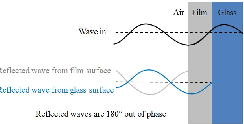
A second effect thin film AR coatings use is destructive interference of reflected light waves. Consider again the air-film-glass optical system. When light intersects the air-film boundary, a wave of light will be reflected. When light travels from a low index medium to a higher index medium, the reflected light wave will experience a 180° phase shift. Light traveling from a high index to a lower index material will experience no phase shift. Therefore, since
nair < nfilm < nglasseach reflected wave will experience a 180° phase shift. If the thickness of
the film is ¼ of the wavelength of the reflected light, the wave reflected from the air-film interface will destructively interfere with the wave reflected from the film-glass interface reducing reflection further in addition to index matching (Equation (1-2)). This effect is shown in Figure 1-1.
4
The top wave in Figure 1-1 shows the light wave traveling from air through the film and glass sections. The two waves below show each reflected wave (only small percentage of original wave because of index matching effect). Both reflected waves have a 180° phase shift and because the film thickness is ¼ wavelength of the incoming light, the waves are 180° out of phase from each other resulting in destructive interference.
The two mechanisms described for thin film AR coatings, index matching and destructive interference, are based on assumptions that the light is normal to the surface and has a single wavelength. This assumption ignores the change in distance traveled through the film with change in incident angle and the fact that natural light is composed of multiple wavelengths. Suppose a thin film AR coating is installed on the front cover of a solar panel. As the day progresses, the relative position between the sun and earth changes so the efficiency of the coating will drop as the sun rises or sets. Also, full spectrum light is composed of light of multiple wavelengths and although multiple AR film layers can be deposited for different wavelengths, this method is not ideal.
1.2.2
Anti-Reflective Nanostructured Surfaces
5
Figure 1-2. Nano-Feature Array of Peacock Butterfly SEM image [7].
The features typically have a maximum height, h, around 250 nm. The spacing between features, d, is generally between 175 nm and 250 nm. Stavenga et al [7] published simulations showing different feature profiles and heights, and the impact on reflectivity over the wavelength, λ, range of visible light, 300 – 700 nm. This study uses the theory that the moth eye features create an optical layer where the ratio of material to air varies with distance from the top of the features to the base of the features. This ratio of air to material is directly related to the index of refraction. As a result, the index of refraction changes over the optical layer from that of air, 1, to that of the substrate material gradually through the optical layer [8] and is referred to as graded index, effective medium or sub-wavelength structure (SWS). The graded index can be modeled based on the geometry of the features and the spacing of the features by taking the optical surface and dissecting it into many sub-layers. An average index of refraction can be calculated for each sub-layer and then the
6
optical surface can be treated as stacked layers of thin film. Figure 1-3 shows how the optical surface can be divided into these sub-layers.
Figure 1-3. Cross section of optical layer dissected into thin sub-layers for analysis [9].
An analysis of the graded index shows that taller features reduce reflectivity in moth eyes from around 4% (for 50 nm tall features) to less than 1% (for 250 nm tall features) across the entire visible light spectrum for all feature shapes examined [7]. Most nanostructured AR surfaces used features which are tapered as shown in Figure 1-3. This shape enables the gradual, continuous variation of the effective index of refraction [10]. The tapered pillar shape is also structurally advantageous to a vertical pillar in that it avoids instabilities in buckling and bending [11]. Research has been conducted into other shape profiles other than the linear taper shown in Figure 1-3. Gaussian, Klopfenstein [10], and needle-like structures were all investigated and showed some differences in results. However, shapes with difficult curvatures may not be realistic in terms of fabrication.
7
the visible spectrum while larger spacing (greater than 300 nm) is more effective at higher wavelengths. This would imply that to achieve an anti-reflective surface it would be desirable to have features whose spacing is between 200 and 250 nm which is representative of the period on moth’s eyes. Figure 1-4(b) is a topographical map for anti-reflection of the nanofeatures with varying height and period. It would appear from this plot that a period between 200 and 300 nm and height of at least 300 nm would be optimum, but it should be noted that the wavelength for this plot is in the near infrared range of 1000 nm.
Figure 1-4. reflective property for different feature height and period. (a) reflective property over full spectrum and varying period with 400 nm height. (b)
Anti-reflective property varying height and spacing for 1000 nm wavelength [12].
8
light reflected from the surface. Increasing the amount of light transmitted to the cell will help reduce both. The index of refraction of silicon is approximately 4.0 which is very high resulting in Fresnel reflection (Equation (1-1)) on the order of 30%.
A study by Toyota [14] included reflectance measurements on moth eye structures over incident angular range of 5° to 80° using a He-Ne laser (632.8 nm wavelength) laser as a light source. The results showed reflectance of less than 1% for angles between 5° and 55° [14]. Other experiments have also been performed where silicon substrates were textured with nanostructures [1]. The period of the nanofeatures in this instance was 150 nm and the overall feature height was 350 nm. Reflection from a 400 nm wavelength source was reduced from 54.7% for the bare substrate to 0.5% for the substrate with nanofeatures. Koynov [15] showed that covering photovoltaic cells with black textured coatings increased photocurrent between 36-42%. These results confirm that nanostructured surfaces improve anti-reflectance not only over multiple wavelengths of light, but also over a broad range of incident angles.
1.3
S
UPERHYDROPHOBICS
URFACES9
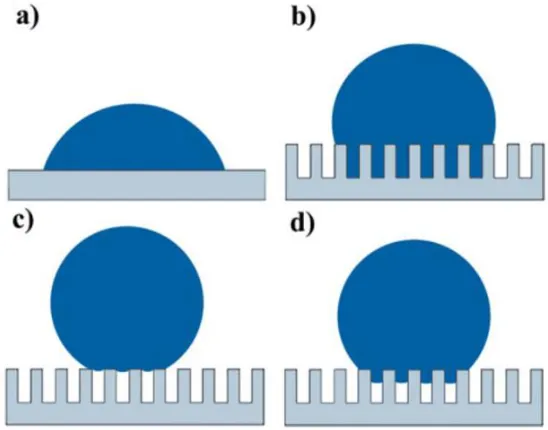
Figure 1-5. Description of contact angle for droplet showing (a) normal (b) superhydrophobic and (c) superhydrophilic behavior.
The wetting behavior of a surface is characterized by the contact angle (CA) of a liquid droplet (use water for description) on a flat solid surface as seen in Figure 1-5(a). This figure shows normal behavior for a droplet on a surface. Surfaces like the lotus leaf with CAs in excess of 150° are described as superhydrophobic and cause droplets to have minimal contact with a surface as shown in Figure 1-5(b) allowing them to easily roll. When a surface causes droplets to have CAs close to 0° as shown in Figure 1-5(c) the surface is called superhydrophilic [20]. While superhydrophilic surfaces do have useful applications, superhydrophobic surfaces are of greater importance because of the self-cleaning property.
10
Figure 1-6. SEM image of hierarchal structure of lotus leaf showing (a) multiple micron-scale features (b) single micron-micron-scale feature and (c) nanometer-micron-scale hairs [21].
An image of the multi-scale structures can be seen in Figure 1-6. Figure 1-6(a) shows many of the micron-scale features on the surface of the lotus leaf that appear to be randomly positioned with similar size and spacing. Figure 1-6(b) shows a single micron-scale feature whose width can be approximated as 10 µm from the scale bar. Figure 1-6(c) shows the nanometer-scale hair-like features that completely cover each of the micron-scale bumps. This special type of surface roughness creates the hydrophobic effect and is described using the Cassie-Baxter model.
There are two models that are generally used to determine the CA of a droplet on a roughened surface which are the Cassie-Baxter (Cassie) and Wenzel equations. These models determine how the droplet will sit on the roughened surface as shown in Figure 1-7. Figure 1-7(a) shows normal contact between a liquid droplet and a flat solid surface. Figure 1-7(b) shows wetted contact between a roughened solid surface and a liquid droplet. The contact is described by the Wenzel equation
11
where θW is the contact angle (CA) of the droplet in the Wenzel mode, r is a surface
roughness factor and θ is the contact angle of the droplet on a flat surface (Young’s model). The hydrophobic behavior illustrated in Figure 1-7(c) is described by the Cassie equation
cosC 1 fs(cos1) (1-4)
where θC is the CA of the droplet in the Cassie mode, fs is the area fraction of the solid at the
surface and θ is the Young’s contact angle. It can be seen that the CA of a droplet will increase as the area fraction of the solid decreases. There is, however, more to the design of nanostructures capable of producing wetting effects than just the Cassie and Wenzel models.
Figure 1-7. Effects of surface roughness on liquid droplet. (a) Liquid droplet on flat surface (Young’s model) (b) wetted contact on rough surface (Wenzel) (c) hydrophobic contact on
rough surface (Cassie) and (d) intermediate between Cassie and Wenzel [20].
12
model and solid area fraction for the Cassie model. The roughness factor is the ratio of the true contact area to the apparent contact area. There is more to be considered when designing an array of nanostructures to produce a hydrophobic effect than just the Cassie model. The Cassie model describes water droplets supported partially by the solid texture and partially by the vapor (air) trapped beneath the droplet in the voids of the texture. Increasing the aspect ratio (larger height to width of nanofeatures), feature density and topography all are important in creating functional superhydrophobic surfaces [11].
13
Figure 1-8. Lotus leaf nanostructures created by (a) Bhushan [22] (b) Sun [23] (c) Liu [24] (d) and Pozzato [25].
1.4
M
ULTIFUNCTIONALS
URFACES14
features were tested with various heights, a 380 nm diameter and approximately 500 nm spacing.
Figure 1-9. Multifunctional features created by Min [19]. (a) A 4 in. silicon wafer with one half covered with features (b) features after 10 min of etch (c) features after 50 min etch and
(d) feature depth vs. etch time.
15
reduction in reflection over the visible spectrum and near IR. The CA of water droplets was also tested for the 380 nm diameter, 500 nm spacing features of varying height. Ten minute etch features (approximately 400 nm tall from Figure 1-9) showed a CA of 110° which was increased to a superhydrophobic state (>150°) for 20 minute etch features (approximately 750 nm tall). Increasing the height of the features past 750 nm did increase the CA but much less than the jump from 400 to 750 nm. The behavior indicates a height threshold that determines when the features are tall enough to trap enough vapor to support droplets in a superhydrophobic state. Other studies [26-29] have shown similar results and could be useful in designing structures for use in nanocoining experiments.
1.5
S
URFACEE
NHANCEDR
AMANS
CATTERING(SERS)
Raman scattering, which was discovered approximately 80 years ago, is a technique of determining the composition of solids, gases and liquids [30]. Raman scattering is the inelastic scattering of light by optical phonons in solids and molecular vibrations [31]. Photons are directed onto the medium of interest and excite the vibrational modes of the molecules. An incident photon interacts with the material and the scattered photon can leave the material at the same frequency (elastic Rayleigh scattering), at a smaller frequency (inelastic Stokes process) or at a higher frequency (inelastic anti-Stokes process). During Raman spectroscopy, the Rayleigh scattered photons are removed because they do not have any information about the sample. If the scattered photon is at a lower frequency, a Stokes process has occurred and quantum energy has been added to the scattering medium. If the scattered photon is at a higher frequency, an anti-Stokes process has occurred and quantum energy has been removed. The intensities of the Stokes energy shifts are thus the characterizing feature of the medium of interest.
16
wavelength range so UV and near IR laser sources are best suited for Raman scattering. Either a holographic notch filter or a dielectric edge filter can be used to reject the elastic Rayleigh scattering. This is critical because the Rayleigh scattering intensity is significantly higher than the Stokes scattering; the ratio is often times larger than 109. Another component in Raman scattering equipment is a detector that can determine the energy (wavelength) shifts between incident and scattered photons. Raman scattering, however, is a weak process due to the small amount of Stokes scattering making it difficult for use in highly sensitive measurements [30].
Surface enhanced Raman scattering (SERS) was first observed in 1974 when an unusual intensity of Raman signals was detected for pyridine adsorbed on a rough silver electrode [32]. The signal intensity of measurements using SERS has been reported to be tens of orders of magnitude greater than that of Raman scattering alone (1013) [30,33]. Because of the enhanced sensitivity SERS can be used for single molecule detection which is attractive in the chemistry, biology, medicine, pharmacology and environmental science fields [34]. SERS has been demonstrated to detect poisonous chemical agents such as cyanide and VX in water [32]. This could be useful in a compact form for battlefield water supply analysis. Another example of the application of SERS is in real-time glucose level sensing in diabetes patients which has the potential to continuously monitor glucose levels (avoiding spikes) as well as eliminate painful finger pricks [32]. The wide variety of SERS applications makes this a rapidly expanding technology.
17
laser and scattering Raman fields. The chemical enhancement is inferred from the measurement because of some behavior that disagrees with the electromagnetic effect. Some molecules differ in amplification by factors of 200 which should not occur since the electromagnetic effect is nonselective [32]. The amplification of some molecules has been explained as a resonance mechanism in which new electronic states arise from chemisorption and have a resonant effect on the Raman scattering although this enhancement is weaker than the electromagnetic effect. Both effects, however, are caused by the introduction of surface roughness on a metallic substrate and nanocoining could be a technique to create the roughness.
Nanocoining is a process of creating features similar to those found in current SERS research. The fact that nanocoined features are ordered would be attractive since some researchers have found that random arrangement of features can cause ‘hot spots’ of SERS effectiveness [36].
18
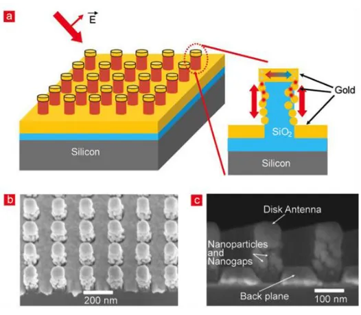
An example of nanofeatures created for a SERS application can be seen in Figure 1-10. These structures were tested and showed an enhancement of 1.2 x 10⁹ in signal intensity while maintaining large-area uniformity with variation less than 25% [37]. There are numerous examples of SERS applications with experimental data to support the enhancement from nanostructures and could be a potential application for nanocoining.
1.6
E
NHANCEDH
EATT
RANSFERC
OEFFICIENT INP
OOLB
OILINGNanofeatures have already been shown to increase the energy efficiency of solar cells, but they have also been shown to save energy in pool boiling applications. There is an ever increasing market in electronics cooling with the requirement of smaller and faster components. Increases in heat transfer demand that surfaces allow large heat fluxes to pass to the surrounding medium. This will be required for advanced laser, advanced radar and power electronic systems [38]. To increase the heat transfer between components and cooling liquid, a high heat transfer coefficient (HTC) is desired. Research has shown [38-43] that introducing nanofeatures onto the heated surface which is in contact with a liquid can increase the HTC significantly. A schematic of pool boiling can be seen in Figure 1-11.
19
The HTC between the heat source and liquid interface shown in Figure 1-11 is typically quantified by measuring the temperature of the liquid, Tsat, and the temperature of the heated
surface, Tsur, where the difference between the two is referred to as the wall superheat. The
amount of power input to the liquid (heat flux), q’’, is generally provided using an electric resistance heat where the power is equal to
'' VI
q A
(1-5)
where V is voltage, I is current and A is the area of the heat source interface with the liquid. The measured temperatures and heat flux can then be used with the convective heat transfer equation to produce an expression for the HTC
( sur sat)
VI h
A T T
(1-6)
20
Figure 1-12. Typical boiling curve for water at 1 atm [44].
21
Research has shown that nanostructures are capable of increasing the CHF while reducing the wall superheat. According to Hendricks et al [38] “The boiling process depends on and is enhanced by three factors: (1) Existence of random micro- or nano-sized crevices and surface irregularities for nucleation initiation, (2) a somewhat porous surface structure that allows fluid inflow to keep nucleation sites active, and (3) surface protrusions that create more active boiling area.” Vemuri and Kim [40] agree with this claim that nanostructures act as nucleation sites and assist in vapor entrapment volume. Li et al [41] also support the idea that the HTC can be increased by adding nanostructured surfaces with the goal of increasing the active sites for nucleation. In fact, results from Li et al’s research showed an increase in HTC of over 17 times as shown in Figure 1-13(a).
Figure 1-13. (a) HTC vs. heat flux for surfaces with varying degrees of nanostructures and a reference surface (solid line, no marker) and (b) nanostructured macro porous (NMP) and
reference surfaces heated by same source [41].
22
HTC for the surface with the triangle markers over the reference surface. Figure 1-13(b) also shows an experiment by Li et al where a circular copper disk was heated in a liquid at a constant heat flux of 1 Wcm-2. One quarter of the disk was covered with nanostructures while the remaining portion was untreated copper. The photograph shows that the copper reference portion remains in a state of natural convection (no bubbles) while the structured portion is in a vigorous state of boiling. This is due to the higher HTC brought on by the nanostructures.
1.7
C
URRENTP
RODUCTIONT
ECHNIQUESAlthough the advantages of using nanostructures for anti-reflective surfaces have been thoroughly defined, a method for producing usable quantities in a realistic amount of time has not been established. Some have been successful at producing a small quantity of nanostructures using methods such as transfer by mold, material ablation and material growth but all suffer from slow manufacturing restrictions. While these methods have not shown the throughput that a product needs to be low cost, one has produced high quality features.
Lithography is the most widely used method for fabricating nanostructures. This method involves using a mask with a specific pattern (in this case the nanostructures) to selectively transfer the pattern to the finished product. Interference lithography is the most common type of lithography used to create arrays of nanostructures.
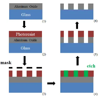
23
After the etching compound has removed the aluminum oxide the remaining photoresist washed off and all that remains is the original substrate with aluminum oxide nanofeatures as shown in step 6. While the process described in Figure 1-14 is a basic lithography process, it does not encompass every technique available.
Figure 1-14. Lithography process basic steps.
24
shape, size and ordering. They also have a high aspect ratio which will increase the anti-reflective property.
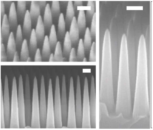
Figure 1-15. Nanofeatures created using laser interference lithography. Scale bars are 200 nm [11].
25
wave which was exposed to photoresist for 5 minutes each. Next a series of etching steps were carried out to remove material from the multiple layers which took approximately 1 hour. Better performance was attained by patterning both sides of the wafer, but the steps described about are enough to prove the point that this process is quite time consuming. It is the objective of the nanocoining process to create nanofeatures like the ones shown in Figure 1-15 while reducing the production time.
1.8
N
ANOCOININGD
EFINITIONThe method proposed to address the need for a rapid production method for sub-micrometer, nanostructured surfaces is called nanocoining. The process of nanocoining involves pressing a diamond indenter with a mold pattern into a work-piece surface until the stress is high enough to induce plastic flow. The indenter is forced until the work-piece material fills the voids of the mold. The indenter is then withdrawn and the plastically deformed shape remains on the work-piece. This process can be seen in Figure 1-16.
Figure 1-16. Nanocoining process where an indenter (a) is pressed into a work-piece causing material flow (b) until the mold is full (c). The indenter is then removed leaving
26
The process shown in Figure 1-16 is repeated until the desired area has been completely covered with nanofeatures. This means the indenter must be precisely indexed in the up-feed and cross-feed directions. The nanocoining process is a physical transfer process as opposed to lithography techniques which are photonic and chemical in nature.
1.9
P
ROBLEMS
TATEMENTThe goal of this research is to produce large areas of nanostructured surfaces in a short period of time using a new process called nanocoining. This technique involves using a diamond indenter with a nanostructured area (20 x 20 µm in this research but not limited) to completely imprint areas on the order of 1 m2. Because the area of the indenter is so much smaller than the total indentation area, an ultrasonic actuator must be used to indent at a high rate. The target rate of 50 kHz requires that the actuator be a resonant device since achieving motion on the order of micrometers at this frequency is difficult otherwise. Indenting at high rates brings about other difficulties such as distortion and precise indexing. Distortion will occur when the indenter and work-piece have relative motion between each other tangent to the work-piece surface. Precise indexing refers to completely covering the work-piece surface with the square indents, much like tiles on a floor. To do this the spindle, cross-feed axis and actuator must be synchronized to a high tolerance. Material effects must also be examined to understand how different material properties will affect the nanofeatures formed. The nanostructured face of the diamond indenter must be square to the surface of the mold so the die will have to be precisely adjusted in three angular directions to transfer the features effectively. It is also imperative that the depth of each indent be constant which is difficult to maintain over large areas. There are many parameters in nanocoining that must be addressed for the process to be successful.
The goal of this work is to implement nanocoining into a manufacturing setting. To accomplish this, the following tasks must be completed:
27
Determine how different materials will react to nanocoining. Optimize diamond die for high quality nanofeatures.
Develop method for mounting and aligning die to test surfaces.
Create nanostructured indents using actuators and precision manufacturing equipment.
Measure and analyze indented test pieces.
Understand how material behaves when indented at the nano-scale.
28
2
INDENTATION BACKGROUND
The indentation process must be modeled before nanocoining experiments can be performed so that the material behavior and required forces can be understood. Indentation involves pressing an indenter (die) into a work-piece. The indenter must have a modulus of elasticity much greater than that of the work-piece to avoid deformation. The goal is to transfer the geometry of the indenter in the region of contact to the work-piece.
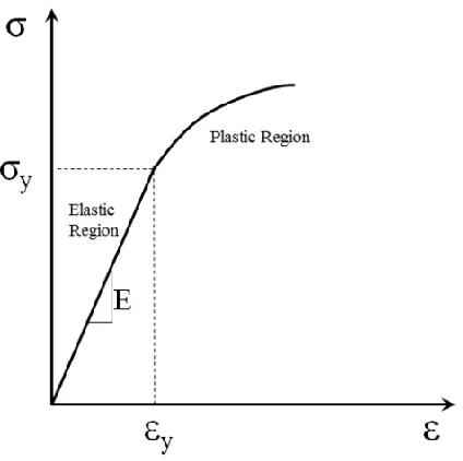
Hertzian contact models cannot be used because they assume both work-piece and indenter behave as fully elastic materials. Indentation is an elastic-plastic process described by two portions of the stress vs. strain (stress-strain) curve. As the indenter is pressed into the work-piece, stresses develop in both the indenter and work-piece. The stress, σ, in the work-piece material will begin in the elastic zone as shown in Figure 2-1.
Figure 2-1. Typical stress-strain curve for engineering materials.
Once the stress reaches the yield stress, σy, of the work-piece, the stress is now described by
29
indentation test is almost immediately in the plastic region of the stress-strain curve due to the small area of the indenter. The stress-strain relationship in the plastic region is typically described using a power law with a strain hardening parameter, n [45].
n
y y
(2-1)
Once the indenter has been removed from the work-piece, permanent deformation can result depending on the amount of force that was applied. A typical output for a nanoindentation test is a plot of force vs. indentation depth. Figure 2-2 shows a comparison between the stress-strain curve and force-depth curve during the loading and unloading phase. During the loading phase, both plots show a transition from an elastic region (linear) to a plastic region (non-linear). Once the indentation is complete, the die is removed from the work-piece causing a linear trend in the unloading section of both plots in Figure 2-2.
![Figure 1-2. Nano-Feature Array of Peacock Butterfly SEM image [7].](https://thumb-us.123doks.com/thumbv2/123dok_us/1597357.1197216/31.612.134.498.67.343/figure-nano-feature-array-peacock-butterfly-sem-image.webp)
![Figure 1-8. Lotus leaf nanostructures created by (a) Bhushan [22] (b) Sun [23] (c) Liu [24]](https://thumb-us.123doks.com/thumbv2/123dok_us/1597357.1197216/39.612.97.534.72.276/figure-lotus-leaf-nanostructures-created-bhushan-sun-liu.webp)
![Figure 1-9. Multifunctional features created by Min [19]. (a) A 4 in. silicon wafer with one](https://thumb-us.123doks.com/thumbv2/123dok_us/1597357.1197216/40.612.135.496.132.423/figure-multifunctional-features-created-min-silicon-wafer.webp)
![Figure 1-12. Typical boiling curve for water at 1 atm [44].](https://thumb-us.123doks.com/thumbv2/123dok_us/1597357.1197216/46.612.168.469.74.369/figure-typical-boiling-curve-water-atm.webp)