ABSTRACT
Mohammed, Mohammed Gamal Abdel Naser . A Study of Eutectic Gallium Indium Liquid Metal in Microsystems and Interfaces. (Under the direction of Dr. Michael Dickey.)
This dissertation studies the behavior of the eutectic alloy of gallium and indium
(commonly called EGaIn) in microfluidic channels, on thin metal films and with metal
powders. EGaIn is a metal alloy that is liquid at room temperature, has high surface tension
and low viscosity. EGaIn forms in presence of oxygen a thin robust oxide skin that allows the
liquid metal to take non-spherical shapes despite its high surface tension. The first chapter
discusses properties and applications of liquid metals in general and EGaIn in more details.
The second chapter studies the phenomenon of spectral colors that appear on PDMS
microchannels filled with EGaIn upon applying a compression strain on it. The channels are
sealed using oxygen plasma which alters the surface chemistry by attaching oxygen atoms to
it and forming a thin rigid film. Buckles form on that thin rigid layer when the channel is
compressed due to the difference in elastic moduli between the film and the bulk of PDMS.
Optical microscopy and AFM confirmed the presence of the buckles. The third chapter
presents a new method for producing liquid metal droplets by forcing EGaIn into reservoirs
with designed dimensions. The dimensions of the reservoir can be easily manipulated to
produce the desired drop size. We can collect the drops or embed them in PDMS. The fourth
chapter studies the behavior of these drops upon contacting metal films. EGaIn drops self-run
on weakly-bounded metal films to substrate in media that continuously etch its oxide skin
like acid solution or under reducing bias. Our experiments show that EGaIn drops achieve
the highest velocities on films of Ag over Au on glass substrates. The running mechanism is
novel and has not been reported before, the liquid metal drop pulls the film from the substrate
film creates an electrochemical cell that leads to formation of hydrogen bubbles beneath the
metal film, the bubbles make the film loose and easy for the EGaIn drop to pull. We
investigated the role of drop diameter to film width ratio and the degree of saturation with the
other metal on the speed of the drop. The velocity we report is higher than that of any
self-running liquid metal drop and any aqueous creature. Self-self-running drops have potential
applications such as fabricating self-destroying electronic circuits. The fifth chapter explores
a new method to create metal micro and nanostructures at ambient conditions by imprinting a
paste made by mixing gallium and metal powders against molds. Gallium and metal powder
interdiffuse in a short period of time and form a solid alloy. In this study we use copper
powder as it is not expensive, safe to work with and can form a solid alloy with gallium at
room temperature. We investigated the optimum mixing ratio (65 wt% Ga and
35 wt% Cu) that allows easy mixing, enough workable time and results in a solid alloy as
diffusion proceeds. The paste can replicate relatively big features (features on a penny for
instance) and create free standing structures, however imprints of small features suffers from
imperfections. Milling and reducing the powder under inert atmosphere helped to enhance
mixing. We are currently studying the effect of particle size on replication and homogeneity
© Copyright 2015 by Mohammed Gamal Abdel Naser Mohammed
A Study of Eutectic Gallium Indium Liquid Metal in Microsystems and Interfaces
by
Mohammed Gamal Abdel Naser Mohammed
A dissertation submitted to the Graduate Faculty of North Carolina State University
in partial fulfillment of the requirements for the Degree of
Doctor of Philosophy
Chemical Engineering
Raleigh, North Carolina
2015
APPROVED BY:
__________________________ __________________________
Michael Dickey Gregory Parsons
Chair of Advisory Committee
__________________________ __________________________
DEDICATION
This dissertation is dedicated to my parents, wife and kids for being always very supportive
and encouraging. I hope I made you proud.
ةلاسرلا هذه يدهأ َّيدلاول
نيبيبحلا و
ل يتجوز يبرد ةقيفر ىيحي ينبإو ميرم يتنبإو
يل اومدقو ينودناس املاط نيذلا
BIOGRAPHY
Mohammed Mohammed was born in Giza, Egypt and he grew up with two sisters and
one brother. He joined the Chemical Engineering Department at Cairo University as an
undergraduate student in 2002 and got his bachelor degree in 2007. He worked in the same
department as a teaching and research assistant for three years. His did research on modeling
and simulations on reactor and industrial chemical process. He got his Master degree in
Chemical Engineering from the same department in Summer 2010. Mohammed started his
PhD program in Department of Chemical and Biomolecular Engineering at North Carolina
State University in Fall 2010. Under the supervision of Dr. Michael D. Dickey he studied the
behavior of liquid metal alloys in microfluidic channels, on thin metal films and with metal
powders. Mohammed is joining Dr. Rebecca Kramer’s group in Purdue University as a
ACKNOWLEDGEMENTS
First of all I want first to thank and praise Allah the most gracious and most merciful
for all his uncountable bounties and blessings.
I want to acknowledge my adviser Prof. Michael Dickey for being very helpful,
supporting and encouraging. I learned a lot in the five years I spent in his research group and
I am thankful for all the great discussions, advices and support. I can never thank him
enough. Also I acknowledge my research group for keeping a friendly and productive
environment, special thanks go to Sharvil, Dishit, Collin and the undergrads for their hard
work on our collaborated projects. I am grateful to Dr Parsons, Dr Maria and Dr Walker for
serving as my committee members. Thanks are due to Dr. Parsons, Dr Maria, Dr Velev and
Dr Spontak for being so kind to let me use their lab equipment. I want to thank Dr Jacob
Jones and his research group for their collaborative work, special thanks to Jonathon Guerrier
for being so collaborative.
Thanks to my parents and parents-in-law for being always very caring and supportive,
you taught me a lot and I could never achieve my goals without you. I appreciate all what
you did and hope I made you proud. My deepest gratitude to my lovely wife Rehab, I can
never dream of a better life partner and I can never imagine my life without you. Your love
and support are a big part of this achievement. Thanks to my little kids Mariam and Yahia for
filling my life with happiness and joy.
I am thankful to all my Egyptian friends and all the members of the Egyptian Student
Association for the happy times we spent together and for their help to pass hard times. I will
my former roommates M. Nafadi, M. Mousa and my friends T. Hamouda, K. Elsayed and A.
TABLE OF CONTENTS
LIST OF TABLES ... ix
LIST OF FIGURES ... x
Chapter 1: Introduction ... 1
Abstract ... 2
1.1 The need for liquid metals in soft, stretchable, and flexible electronics ... 3
1.2 Low melting point metals and their applications ... 5
1.3 Gallium and Low-Melting Point Gallium Alloys ... 7
1.4 Oxide Skin of Eutectic Gallium Indium Alloy (EGaIn) ... 9
1.5 Applications of EGaIn ... 12
1.5 Motivation and Layout of the Dissertation ... 19
1.6 References ... 21
Chapter 2: Strain-controlled Diffraction of Light from Stretchable Liquid Metal Micro-components ... 31
Abstract ... 32
2.1. Introduction ... 33
2.2. Results and Discussion ... 35
2.3. Conclusion ... 42
2.4. References ... 44
Chapter 3: Production of Liquid Metal Spheres by Molding ... 48
Abstract ... 49
3.1 Introduction ... 50
3.2 Experimental Design ... 53
3.3 Results and Discussions ... 55
3.4 Conclusion ... 62
3.5 References ... 64
Abstract ... 70
4.1 Introduction ... 71
4.2 Results and Discussion ... 73
4.3 Summary ... 87
4.4 References ... 88
Chapter 5: Gallium-Copper Paste for Room Temperature Imprinting. ... 93
Abstract ... 94
5.1 Introduction ... 95
5.2 Discussion ... 98
5.3 Current and Future Work ... 107
References ... 109
Chapter 6: Summary and Outlook ... 114
6.1 Summary ... 115
6.2 Future Outlook ... 118
APPENDICES ... 120
Appendix 1 ... 121
A-1.1 Figures confirming the effect of oxygen plasma on buckles and diffraction ... 121
A-1.2 Laser pointer test on permanent soft gratings ... 123
A-1.3 Measuring Buckles Dimensions ... 127
Appendix 2 ... 129
Appendix 3 ... 130
A-3.1 EGaIn on gold film ... 130
A-3.2 Behavior of bilayered films of silver over gold in acid solutions ... 132
A-3.3 Contact angles of the drop with the film and the substrate ... 135
A-3.4 References ... 137
Appendix 4 ... 138
A-4.2 EDS mapping of Ga-Cu alloy pealed from PDMS mold ... 141
A-4.3 Solid Ga-Cu alloy by melting ... 142
LIST OF TABLES
Table 1.1. List of low melting points metals. ... 6
Table 1.2. Physical properties of liquid gallium, EGaIn, Galinstan and water ... 9
Table 4.1. Comparison between speeds of current self-running EGaIn droplets and other self-moving liquid metal droplets in literature ... 85
LIST OF FIGURES
Figure 1.1 Examples of flexible electronics (a)flexible display, (b) flexible LED’s, (c) flexible chip for hear monitoring and (d) flexible electrode for supercapacitors. ... 4
Figure 1.2. Curved and wavy metal structures in elastomers for flexible electronics (a) stretchable interconnect, (b) electronic eye camera, (c) stretchable batteries, (d,e) integrated circuit and (f) epidermal electronics ... 5
Figure 1.3. Periodic table showing the elements that can form alloys with gallium . ... 8
Figure 1.4. a) Auger spectroscopy peaks of EGaIn surface oxide showing the its composition and b) TEM images of EGaIn nanospheres with an inset on the oxide ... 10
Figure 1.5. a) Comparison between behavior of EGaIn and Hg when injected in microchannels, oxide on EGaIn keeps it stable while Hg retracts, b) An EGaIn drop bifurcates when touched with a rod and pulled out and c) EGaIn “dolls” made by stacking EGaIn drops. ... 11
Figure 1.6. a) Side view images of EGaIn in parallel plate rheometer showing the top rotating plate and the bottom stationary plate, the oxide is stretched as the rheometer rotates left and right, and b) A plot of viscous modulus and elastic modulus of oxide skin as a function of surface stress. ... 12
Figure 1.7. Examples of EGaIn-filled flexible antennas. a) Flexed dipole antenna, b) radiofrequency antenna and c) Loop antenna. ... 13
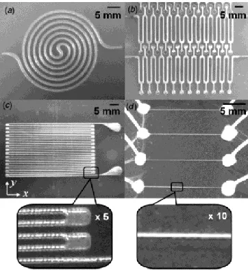
Figure.1.9. Different shapes of microchannels of soft elastomer ECOFLEX filled with liquid metal used for pressure sensing by relating the resistance change to the pressure applied. a) Spiral channel, b) serpentine-shaped channel, c) strain gauge, d) small liquid structures. ... 15
Figure 1.10. Flow focusing of liquid metal with glycerol solution to create liquid microspheres. a) Top-down microscope image of the microchannel with EGaIn microspheres flowing inside, b) a glass bottle filled with monodispersed EGaIn microspheres, and c) EGaIn non-spherical micro rods. ... 16
Figure 1.11. Two patterning techniques for liquid metals on elastomeric substrates. a) Direct laser patterning steps and examples of different metal patterns enclosed in elastomer and b) Steps to microcontact printing using a mask to selectively pattern the metal and an image of the product after encasing in the elastomer. ... 17
Figure 1.12. Additive patterning techniques produce (a) free standing 3D structures, and (b) conformal 2D. ... 18
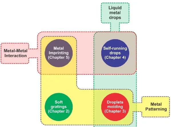
Figure 1.13. Diagram showing the three main themes that unite the work presented in this dissertation ... 20
Figure 2.1. A photograph of a PDMS microfluidic channel filled with EGaIn. Flexing the structure causes the surface of the metal to reflect a spectrum of colors. ... 34
Figure 2.2. Different approaches for fabricating diffraction grating (a) by replica molding against a master mold, (b) laser micromachining and (c) using a fluid injected in narrow microchannels. ... 35
Figure 2.3. Liquid metal on the internal wall of a PDMS microchannel (a) uncompressed showing metallic reflectivity (b) compressed to 13% strain, which induces the appearance of color from the surface of the metal. ... 37
plasma. The two drops of EGaIn were placed on the PDMS before and after releasing the strain. ... 38
Figure 2.5. (a) An AFM image of the buckles formed on the surface of 20% prestrained PDMS after exposure to an oxygen plasma and release of the strain (b) Zero (m=0) and first order (m=1) diffraction peaks formed by shining a red laser through PDMS featuring a buckled surface. ... 41
Figure 2.6. Dark field, top down micrographs of the metal surface in an EGaIn-filled microchannel (a) before applying large compressive strains (>30%) and (b) after relieving the strain. ... 42
Figure 3.1. A scale showing the range of diameters of droplets produced by sonication, flow focusing and dispensing. ... 52
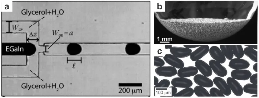
Figure 3.2. Steps for producing EGaIn microspehers. (a,b) A laser writer patterns pillars on a sheet of acrylic. (c) PDMS molded against the acrylic creates an inverse replica. (d) After spraying isopropanol on the surface of the PDMS, another acrylic sheet forces EGaIn into the reservoirs. (e) EGaIn in reservoir is exposed to HCl vapor to remove the oxide skin. (f) EGaIn spheres are released and collected in a stabilizing medium. ... 54
Figure 3.3. (a) EGaIn spheres in a PDMS mold before removing them. (b) EGaIn drops collected and demolded into a petri dish. ... 55
Figure 3.5. (a) A side-view image of a reservoir filled with EGaIn, (b) a side-view goniometer image of the droplet after releasing it from the reservoir, and (c) a top-down microscope image of the same droplet. ... 58
Figure 3.6. (a) Graphical relation between the volume of EGaIn spheres and the actual volume of the reservoir. The lines of slope = 1 and intercept = 0 guides the eye for an ideal agreement between the reservoir and drop volume. (b) A side view of a reservoir overfilled with EGaIn, which appears dark due to the backlighting, (c) Graphical relation for the smallest spheres. The blue dotted lines in the inset graph in plot (a) and in plot (c) graphs are the best linear fit for the data whose slope is the filling factor. ... 59
Figure 3.7. The percent counts of the filling factor of reservoirs with EGaIn. ... 61
Figure 3.8. (a) EGaIn spheres embedded completely in PDMS, (b) a liquid metal drop placed in a liquid metal pump using the molding technique ... 61
Figure 4.1. Examples of the different approaches for creating a gradient in wettability of droplets on surfaces. (a) Thermocapillarity, (b) chemical species gradient, (c) surface structure and (d) reactive wetting. ... 72
Figure 4.2. (a) Snapshots of an EGaIn drop contacting a silver film bonded to epoxy in 2M HCl solution. (b) Snapshots of an EGaIn drop wetting a silver film floating on the surface of 2M HCl solution. The EGaIn pulls the metal film into the droplet (from left to right), where it presumably dissolves. ... 74
Figure 4.3. Schematic side view diagrams of EGaIn drops that accelerate over thin metal films. The metal only accelerates in the absence of the surface oxide, which can be removed by (a) acid and (b) electrochemical reduction. ... 76
Figure 4.4. Top-down snapshots of EGaIn droplet running on traces of 90 nm of Ag on 10 nm of Au with straight and curved geometries. The glass substrate is submerged in 2 M HCl. Scale bar is 5 mm. ... 77
proton reduction and formation of hydrogen bubbles on both sides of the film, (b) Top-down and (c) bottom-up snapshots of a 90 nm silver/10 nm gold film contacted with an EGaIn drop moving right to left in 2M HCl solution. Dotted circles highlight the EGaIn drop. ... 79
Figure 4.6. Bottom-up images of 90 nm Ag / 10 nm Au trace on a glass slide in 1N NaF solution. The small circles indicate the tiny gas bubble formed at -0.7 volts that become more pronounced with more reducing potentials that cause the film to delaminate. ... 79
Figure 4.7. (a) Schematic diagram of the classical profile of a moving drop on a substrate where the drop has two contact angles (advancing and receding angles) with the surface, (b) Schematic diagram of the running EGaIn drops where the film delaminates and the two contact angles of the drop with the film are the same on both sides of the drop. ... 81
Figure 4.8. (a) Snapshots of 1 mm EGaIn drop going uphill at 22 degrees inclination angle on a Ag/Au trace patterned on glass, (b) Measured and theoretical speed of 0.7 mm diameter EGaIn drop running on 1mm width Ag/Au trace at different inclination angles. ... 83
Figure 4.9. a) Plot shows the effect of the ratio of drop diameter to metal film width on speed for drops running on Ag/Au, b) Plot shows the effect of mass percent of Ag and Au in the EGaIn drop on speed for different diameters in 2M HCl on a 2 mm wide film of Ag/Au, c) Top-down images of drops having different diameters on 1.5 mm wide Ag/Au film. ... 84
Figure 4.10. A comparison between the speed of self-running EGaIn drop and the maximum speeds of the fastest known aqueous creatures in units of body lengths per second. ... 86
Figure 5.1. Metallic micro and nanostructures produced by different patterning techniques. (a) direct nanoimprint lithography, (b) transfer printing of metal inks, (c) selective laser sintering of silver nanoparticles and (d) reversal imprinting. ... 96
Figure 5.2. Micro and nanostructures produced by laser-assisted techniques . (a) Laser shock assisted direct imprinting, (b) conical spikes by femtosecond laser pulses and (c) array of nanogears by laser shock imprinting. ... 97
Figure 5.3. Procedure for Ga-metal powder alloy mixing and replicating. ... 99
Figure 5.4. Phase diagrams of gallium with the (a) Ag, (b) Cu, (c) Al and (d) Mg. The red highlighted regions indicate the windows of possible mixing ratios of Ga with the metal powders to form solids at room temperature. ... 100
Figure 5.5. Summary of how soft or hard the copper-gallium paste is at compositions from 48 to 82 weight percent gallium after different periods of time. ... 101
Figure 5.6. Replicas of Ga (65 wt%) and Cu (35 wt %) alloy (a) A penny and (b) gears with diameters 10, 7, 5 and 3 mm ... 102
Figure 5.7. (a) SEM image of Ga-Cu alloy replica of 10 micron wide lines (scale bar=280 m) and (b) SEM image of Ga-Cu alloy replica of features on CD (scale bar=20 m) and the dotted regions in the microscope image (c) show copper particles that did not mix with Ga. ... 103
Figure 5.8. (a) Schematic diagram for milling the copper powder with zirconia balls to shear the powder and (b) Photographic images and SEM images of copper powder before and after milling (Scale bar for SEM images is 50 microns). 104
Figure 5.10. SEM images to the Ga-Cu (65 wt% Ga, 35 wt% Cu) prepared using 70 nm Cu nanoparticles after reduction in the reduction furnace ... 107
Figure 5.11. EDS mapping of solid alloys made from mixing Ga (65 wt %) and copper (35 wt %) with different particle sizes. (Courtesy: Dishit Parekh and Jonathon Guerrier) ... 108
Figure A-1.1. A mercury-filled microchannel composed of PDMS (a) uncompressed and (b) compressed showing faint colors during compression. This result suggests the oxide that forms on EGaIn is not a requisite for observing color. Also, because mercury does not stick to the microchannel during buckling, the color is fainter than that observed EGaIn. ... 121
Figure A-1.2. Light diffraction on the bottom side of an oxygen plasma-treated pre-strained PDMS strip with a drop of EGaIn placed on it before releasing the strain. Light diffraction occurs on both regions (EGaIn-covered and uncovered). Both regions show the same color, which implies the periodicity of buckling is the same with or without the metal. However the EGaIn-covered region looks brighter due to the reflective nature of the metal. ... 121
Figure A-1.3. Microscopic images, AFM images (plan and 3D) and sectional profiles of 20% pre-strained samples treated with (A) oxygen plasma 50 watts for 20 seconds, (B) oxygen plasma 100 watts for 120 seconds, (C) oxygen plasma 100 watts for 180 seconds and (D) UVO for 1 hour. Figure A represents the conditions studied in this paper, which were chosen because they represent the best conditions for sealing microchannels based on empirical evidence. ... 122
Figure A-1.4. Diffraction of laser light on a PDMS substrate pre-strained to 20% strain, oxygen plasma-treated, and released to 0% strain. The buckles diffract as expected. ... 124
Figure A-1.5. Wave guiding of laser light on the surface of oxygen plasma-treated (50 watts for 20 seconds) pre-strained (20% pre-strain) PDMS strip ... 125
watts for 120 seconds, (c) oxygen plasma 100 watts for 180 seconds and (d) UVO for 1 hour. ... 126
Figure A-2.1. Depth of features produced in an acrylic sheet using a laser cutter in raster mode at different powers and speeds. ... 129
Figure A-3.1. Contact angles of EGaIn drop on different metal films in air, after wetting with 2M HCl and exposure to HCl vapor. ... 130
Figure A-3.2. Snapshots of an EGaIn drop contacting a 100 nm gold film on glass slide immersed in 2M HCl. ... 131
Figure A-3.3. Top-down and bottom-up images of a silver (90 nm) over gold (10 nm) film on glass slide after 10 seconds of wetting with a solution of 1M, 2M and 3M HCl. Scale bar is 500 m ... 133
Figure A-3.4. Bottom-up snapshots of a film of Ag/Au on a glass slide after putting a drop of 3M HCl on the top surface of the film. ... 133
Figure A-3.5. Cartoons showing the two hypotheses for transfer of electrons from silver film to gold film in HCl solution. ... 134
Figure A-3.6. High speed snapshot of an EGaIn drop pulling a Ag/Au film while running over it. The advancing and receding contact angles of the EGaIn against the glass slide and its contact angle against the metal film are highlighted in the bottom image ... 136
Figure A-4.1. Schematic diagrams to a drop wetting a structured surface based on (a) Cassie model and (b) Wenzel model and (c) Cartoon showing layers on CD, the dotted lines highlight the dimensions of these structures that we replicate [3] and (d) Profilometer scan to ... 139
of parts of the mold that got teared off on peeling. (Courtesy: Dishit Parekh and Jonathon Guerrier) ... 141
Abstract
This dissertation is a study of the behavior of the low-melting point metal gallium and
the eutectic gallium indium alloy in microsystems such as microchannels, micromolds, and
microscale droplets. Three themes unite the work reported within this dissertation, including,
(1) new methods to actuate liquid metal, (2) new methods to pattern metals at room
temperature, and (3) studies on the interaction between liquid metals and solid metals. There
is growing interest in gallium and gallium-based liquid metal alloys because of the
combination of fluidic and metallic properties; this dissertation enriches this field of research
by studying new behavior of these metals and developing new applications.
This Chapter discusses the unique properties of the Ga and Eutectic Gallium-Indium
alloy (EGaIn) that motivate the work done in this dissertation, in addition to an overview of
the previous research done on gallium, EGaIn and other low melting point liquid metals and
a review of their applications. The applications of gallium and low-melting point gallium
alloys are wide and diverse, examples of which are high temperature thermometers, heat
transfer medium, lubricant for high temperature applications, mirrors, a replacement for
mercury in dental amalgams, soft robots [1–4]. It is hard to cover all these applications in
details so we are chose to discuss in some details the use of gallium alloys in the field of
flexible and stretchable electronics as an example of a fast growing field that is making an
1.1 The need for liquid metals in soft, stretchable, and flexible electronics
Liquid metals offer new opportunities for electronic devices that have unique
mechanical properties. Conventional electronic devices are typically fabricated from rigid
materials. It is possible to make these rigid materials flexible by using thin film form factors.
To the best of our knowledge, the first attempt to make flexible electronics started in the
1967 by the advent of “thin-film electronics” where a silicon film of few hundreds microns
thickness was embedded in a flexible matrix to make a flexible solar cell [5,6]. Even though
silicon is a rigid, brittle material, these structures are flexible due to the thin film factor.
Advanced electronics typically consist of insulators, conductors, and semiconductors. This
thesis focuses on conductive materials. It is possible to make thin-film electronics that are
flexible using thin metal films or inks [7–10]. Thin-film electronics enable other applications
such as displays [11–13], electrodes [14,15], antennas [16], chips for medical applications [17],
light-emitting diodes [18] and wearable electronics [19,20]. Figure 1.1 shows some examples of
flexible electronics.
The devices in Figure 1.1 are flexible, however the films are not inherently
stretchable due to the low fracture strain of most metals. The ability to form electronics that
are stretchable improves the durability of these devices and enables a wider range of
applications. This drawback led to the new approach of fabricating devices with wavy metal
films or mesh structures to increase the stretchability of devices [21–24]. This approach enabled
stretchable interconnects [25,26], integrated circuits [27,28], batteries [29], and epidermal
electronics [30,31]. With proper engineering design, the devices fabricated using this technique
strain of these devices and can lead to the formation of cracks and fractures during long term
use [32]. Studies show that metal films plastically deform with prolonged use leading to
permanent deformation that reduce device efficiency or totally disconnect the circuit [33–35].
Figure 1.1 Examples of flexible electronics (a)flexible display [13], (b) flexible LED’s [18], (c) flexible chip for hear monitoring [17] and (d) flexible electrode for supercapacitors [15].
The drawback of aforementioned fabrication techniques motivates other alternative
like CNT pastes, conductive inks and liquid metals to solid metal films [36–39]. This
dissertation focuses on gallium and low melting point alloys of gallium.
Liquid metals have fluid properties that allow it to be injected in microchannels and
will take the shape of the channel while stretching, bending or flexing without permanent
deformation, hence solving the problem of plastic deformation, cracking, and fracture in the
those that are extremely soft. The following sections discuss the properties and applications
of liquid metals in more detail.
Figure 1.2. Curved and wavy metal structures in elastomers for flexible electronics (a) stretchable interconnect [25], (b) electronic eye camera [40], (c) stretchable batteries [29], (d,e) integrated circuit [22,24] and (f) epidermal electronics [30]
1.2 Low melting point metals and their applications
Metals are characterized by common physical properties such as high electrical and
thermal conductivity, ductility and malleability [41]. Most metals have high melting points
that can go up to 3540 °C [42], however few metals are liquid near room temperature. Table
the metallic properties in novel applications such as soft electrodes, conformal metallic
contacts, microfluidics and deformable electronics. However, the hazards associated with
most of these metals, such as radioactivity, toxicity, and high reactivity limits their use.
Table 1.1. List of low melting points metals.
Metal name Symbol Melting point, oC Health hazards
Mercury Hg -38.83 [43] Toxic [44–46]
Francium Fr 27 [47] Highly Radioactive [48]
Cesium Cs 28.44 [49] Highly reactive and pyrophoric [49]
Gallium Ga 29.77 [49] Low toxicity [50]
Rubidium Rb 39.30 [49] Highly reactive [51]
Mercury is a popular liquid metal and has been used in many applications, the most
famous of which is the mercury thermometer. It has been used for more than 165 years in
dental amalgams as it mixes easily with metal powders forming a paste that hardens after a
short time [52]. Hg is also well suited as a as soft electrode for measuring the capacity of
electrical double layers [53] and to molecules such as DNA that adsorb to the surface of the
metal [54]. The dropping mercury electrode is a technique that pumps Hg out of the end of a
capillary, which ensures a smooth and uncontaminated metal surface that needs no cleaning
or polishing. It is useful and necessary for sensitive electrochemical tests [55–57]. Other
applications include junctions for measuring the electron transport through self-assembled
sensors for detecting heavy metals in solutions [60]. The high surface tension of mercury
enables its use for actuation and micro-pumping [61,62]. Despite these exciting applications,
the use of mercury is often avoided due to its toxic nature [63].
Gallium is considered the least hazardous among the five listed liquid metals. It is
naturally present in the human body [64]. It is approved as a replacement material for mercury
in dental amalgams [1] (although rarely used). Salts of gallium have been approved as a MRI
contrast agent and has proven useful for antibacterial therapy [65] and treatment of cancer [66].
Gallium is considered to have low toxicity however only one case was reported for poisoning
after exposure to gallium halide complexes [50]. Gallium is therefore replacing mercury in
most of its applications and is widely used in emerging applications. The next section
discusses gallium and low melting point alloys containing gallium in detail starting with a
brief historic background, followed by their properties and their current applications.
1.3 Gallium and Low-Melting Point Gallium Alloys
Gallium was first discovered by the French chemist Paul-Émile Lecoq de
Boisbaudran in 1875. It is not present in a pure form in nature. Instead, it is extracted as a
byproduct from aluminum and zinc production [67]. It lies within group 13 of the periodic
table and its atomic weight is 69.716 [68]. It is the element with the widest liquid temperature
range since it normal melting point is 302.98 oK and normal boiling point is 2676 oK [2].
Interest in gallium increased with the discovery of the semiconducting properties of gallium
compounds with group 15 elements, the most famous of which are GaAs and GaN [69].
Gallium is characterized by its high affinity to alloy with a wide range of elements (either
oxides, and sulphides [2]. The elements that gallium can alloy with are highlighted in blue in
the periodic table shown in Figure 1.3 [70].
Some of the elements form binary or ternary eutectic alloys, meaning alloys that have
a melting point lower than the melting points of the separate constituents. The most common
examples of these are EGaIn (75.2% Ga and 24.8% In, weight percent) and Galinstan (67%
Ga, 20.5% In and 12.5% Sn, weight percent). Table 1.2 summarizes the main physical
properties of gallium, EGaIn and Galinstan and compares them to water. In this thesis we
focus on EGaIn in most of the work, taking advantage of its low freezing point and its simple
binary composition. For this reason, this Chapter discusses properties of EGaIn with a focus
on its oxide skin and the published applications of EGaIn. We use gallium instead of EGaIn
only in Chapter 5 for mixing with metal powders for producing metal structures as it is easier
to understand and study binary systems.
Table 1.2. Physical properties of liquid gallium, EGaIn, Galinstan and water [2,71–81]
Gallium EGaIn Galinstan Water
Melting point, °C 29.8 15.5 10.7 0
Boiling point, °C 2402 2000 >1300 100
Density, gm/cm3 6.905 6.36 6.36 1
Viscosity, 10-3 Kg/m.sec 1.969 1.99 2.09 1
Surface tension, mN/m 750 632 718 72.8
Thermal conductivity, W/m.K 30.54 26.43 25.41 0.6
Electric resistivity, 10-6ohm.cm 27.2 29.4 30.3 20E8
1.4 Oxide Skin of Eutectic Gallium Indium Alloy (EGaIn)
The properties of EGaIn listed in table 1.2 motivate its use in fluidic applications.
EGaIn is easy to inject in microfluidic channels due to its low viscosity. Also it has high
electric conductivity, thermal conductivity, and low health hazards. The most important
property of EGaIn that makes it well-suited for many applications is the formation of a very
thin oxide skin spontaneously on its surface in the presence of oxygen. The oxide skin on
gallium is believed to be amorphous -Ga2O3 [82]. Auger spectroscopy analysis of the oxide
skin on EGaIn establishes that in ambient conditions the amount of indium in the skin is very
low as shown in the peaks in Figure 1.4-a [83]; this is attributed to the fact that In oxidizes
Figure 1.4. a) Auger spectroscopy peaks of EGaIn surface oxide showing the its composition [83] and b) TEM images of EGaIn nanospheres with an inset on the oxide
A previous X-ray study on the oxide skin of gallium shows that its thickness is
5 Å [82], however TEM imaging of sonicated EGaIn nanospheres shows it is only 3.33 nm as
shown in Figure 1.4-b. Although the oxide film is extremely thin, it is strong enough to hold
the liquid stable in microchannels despite its high surface tension [82]. Figure 1.5-a compares
EGaIn and Hg when injected into microchannels by applying pressure, and after the pressure
is released. Mercury retracts spontaneously out of the channel as a result of surface tension
while the oxide on EGaIn keeps it stable inside despite having a higher surface tension than
mercury. The oxide is strong enough to allow drops to assume non-spherical shapes like
cones (Figure 1.5-b) or even to stack drops making different shapes like the dolls in
Figure 1.5. a) Comparison between behavior of EGaIn and Hg when injected in microchannels, oxide on EGaIn keeps it stable while Hg retracts [80], b) An EGaIn drop bifurcates when touched with a rod and pulled out [83] and c) EGaIn “dolls” made by stacking EGaIn drops [85].
A parallel plate rheometer quantified the mechanical properties of the oxide that
forms on EGaIn. The instrument consists of two disks that sandwich the metal, the bottom
disk remains stationary while the top rotates back and forth with the desired applied torque as
shown in Figure 1.6-a [86]. The stress and strain are calculated from the torque and the angular
displacement. The measurements show that the oxide yield stress dominates its mechanical
response to stress. Figure 1.6-b plots the elastic modulus (G’) and viscous modulus (G”)
EGaIn as a function of surface stress (s). The plot shows that the oxide has elastic modulus
of 10 N/m which means that it can store stress and return back to its original state. The plot
also shows that the oxide has a yield stress of ~500 mN/m. Below this stress the oxide is
stable and the metal will not flow, however at higher stresses the oxide ruptures and the
Figure 1.6. a) Side view images of EGaIn in parallel plate rheometer showing the top rotating plate and the bottom stationary plate, the oxide is stretched as the rheometer rotates left and right [86], and b) A plot of viscous modulus and elastic modulus of oxide skin as a function of surface stress [80].
The oxide skin can be etched in media with pH higher than 10 and lower than 3 [87].
The liquid metal (in the absence of the oxide) assumes a spherical shape as the surface
tension defines the shape of the liquid. The Ga2O3 skin can also be reduced electrochemically
by applying a reducing bias to the liquid metal in electrolyte solution [88].
1.5 Applications of EGaIn
Utilizing the interesting properties mentioned above, EGaIn has been used in
microfluidic channels for many applications. The liquid nature of EGaIn can be integrated
with the soft nature of elastomeric materials to fabricate soft electronics [89]. For instance
liquid metal can be injected in flexible microchannels made from elastomeric materials such
as polydimethyl siloxane (PDMS) to make antennas that are flexible and stretchable. These
properties enable stretchable antennas with a resonance frequency tuned by strain [90]. Liquid
radiofrequency antennas [92], loop antennas [93] and a coaxial transmission line and phase
shifter [94]. Examples of these devices are shown in Figure 1.7. Microchannels can be
integrated with other devices to make large area radiation sensors [95] diodes and memristors
[96]. EGaIn has been used as soft and flexible interconnects to allow soft and conformal
contact between the metal and the circuit [97,98].
Figure 1.7. Examples of EGaIn-filled flexible antennas. a) Flexed dipole antenna [90], b) radiofrequency antenna [92] and c) Loop antenna [93].
EGaIn injected into microchannels made from self-healing polymers (e.g. polymers
that form hydrogen bonds and heal after tearing and reconnecting [99]) to form self-healing
wires. The wires do not leak the liquid metal when cut as the oxide skin forms spontaneously
and keeps it stable inside the microchannel. The microchannel can be reconnected in
different configurations leading to different circuit designs [100].
Devices based on EGaIn have the advantage of continuous electric conductivity at
extremely high strains. Typically, the yield stress of the elastromer limits the maximum strain
styrene-ethylene-butylene-styrene (SEBS) and filled with EGaIn still function under very
high strains that can go up to 700% [101].
Liquid metal can also be injected in microchannels with posts that will not allow it to
flow because of the oxide skin but will keep it in direct contact with the other side of the
microchannel [102] as shown in Figure 1.8. This is an easy and convenient way for fabricating
soft electrodes that can be put in contact with other fluid that is injected on the other side of
the posts. This strategy has been implemented in applications like electrohydrodynamic
mixing [102], coulter counting [103], pumping [104], valving [105], and stimulating neurons [106].
The deformation in the shape of the microchannel filled with liquid metal affects the
electric conductivity of the channel as the dimensions change. The change in electric
conductivity determines the deformation applied to the channel. For instance EGaIn in very
soft elastomers like ECOFLEX is used as soft sensors for pressure, strain [107] and curvature
[108,109], examples are shown in Figure 1.9. The soft and flexible nature of these devices
allowed use in medical applications like strain sensors that provide walking assistance for
patients without hindering their motion [110]. Two layers of microchannels filled with EGaIn
help give better detection of the local pressure and is used to fabricate wearable keypad [111]
Figure 1.8. Inherently aligned liquid metal electrodes in a microchannel. a) A schematic of the design of the PDMS microchannel with posts showing the sides where the liquid metal is injected, and b) top-down microscope image with back light for the microchannel where EGaIn works as electrodes [102].
Figure 1.9. Different shapes of microchannels of soft elastomer ECOFLEX filled with liquid metal used for pressure sensing by relating the resistance change to the pressure applied. a) Spiral channel, b) serpentine-shaped channel, c) strain gauge, d) small liquid structures [107].
Microfluidic flow focusing has been used to create liquid microspheres. The channel
design forces liquid metal (dispersed phase) to flow between two streams of a mixture of
glycerol and polyvinyl alcohol (continuous phase) as illustrated in Figure 1.10-a [113]. This
continuous phase prevents the liquid metal from sticking to the walls of the channel and
stabilizes the surface to prevent liquid drops merging. Liquid metal can be kept stable by
coating with small particles of other material (tungsten oxide) and creating “liquid metal
marbles” [115]. Liquid micro drops can be enclosed in polymer to make conductive polymer
composites [116].
Figure 1.10. Flow focusing of liquid metal with glycerol solution to create liquid microspheres. a) Top-down microscope image of the microchannel with EGaIn microspheres flowing inside, b) a glass bottle filled with monodispersed EGaIn microspheres [113], and c) EGaIn non-spherical micro rods [114].
In addition to injecting the metal into microchannels, there are other methods to
pattern the metal. For example, direct laser patterning is one method in which PDMS
encases a layer of liquid metal, then a CO2 laser selectively removes the metal from the
undesired regions. The final shape is then encased in more PDMS. Steps of this technique are
shown in Figure 1.11-a. This is an inexpensive subtractive approach that can pattern metals
Microcontact printing is another classical patterning method that has been applied to
liquid metals. This is achieved by spreading a film of EGaIn on the elastomeric surface with
mask to selectively coat the desired areas, or by transferring drop by drop from a pool of
EGaIn to the elastomer surface using a tip [118]. Steps to microcontact printing using a mask
and a final product are shown is Figure 1.11-b.
Figure 1.11. Two patterning techniques for liquid metals on elastomeric substrates. a) Direct laser patterning steps and examples of different metal patterns enclosed in elastomer [117] and b) Steps to microcontact printing using a mask to selectively pattern the metal and an image of the product after encasing in the elastomer [118].
Controlled dispensing of liquid from syringes allowed additive patterning the liquid
metal. Controlled volumes of a liquid drops can be dispensed using a pressure controlled
needle and stacked over each other to pattern the metal. Using this technique the liquid can
this technique are shown in Figure 1.12-a. The controlled flow of liquid metal allows also
direct writing of the liquid metal on surfaces using CAD software, the required design is sent
to the dispensing machine that dispenses the liquid while moving on the elastomer with the
desired pattern keeping a small gap between the needle and the substrate to ensure smooth
uniform lines and prevent liquid accumulations [119]. Figure 1-12-b shows a schematic of the
process.
Figure 1.12. Additive patterning techniques produce (a) free standing 3D structures [85], and (b) conformal 2D [119].
The next section discusses the outline to this dissertation showing the motivation and
1.5 Motivation and Layout of the Dissertation
EGaIn and other liquid metals have many applications in flexible microfluidic
devices like antennas [90,92,93,120], wires [100,101], interconnects [121] and sensors [122]. As
mentioned earlier in this Chapter PDMS is a silicon-based elastomer used widely for
fabricating microchannels as it is easy to mold and perfectly replicates small features, cures
in relatively short times at moderate temperature, and has durable elastomeric mechanical
properties [123]. In addition, air plasma treatment of PDMS changes its surface chemistry by
forming hydroxyl groups ono the surface and allows sticking of PDMS to different surfaces
or another PDMS surface [124] and makes it perfect for fabricating microfluidic channels [125].
Chapter Figure 2 discusses the phenomenon of light diffraction due to the compression of
microchannels filled with EGaIn, explains the factors leading to this phenomenon, and
present potential applications.
Besides studying the behavior of the liquid metal in microchannels we sought to
study its behavior on thin metal films since gallium and gallium alloys have high affinity to a
wide range of elements (cf. Figure 1.2). We studied the behavior of liquid metal drops in
contact with different metal films (silver, gold, copper, aluminum and chromium) on
different substrates in media that allow good contact between the metal drops and the thin
films. Current techniques for producing liquid metal drops like flow focusing [113,126] and
sonication [127,128] produce liquid metal drops with diameters smaller than what we require for
our experiments. Hence, we developed a new method to produce the liquid metal drops.
Chapter 3 demonstrates this novel technique for producing liquid metal drops by molding.
Chapter 5 discusses the interaction of liquid metal with metal powders. The diffusion
between the liquid metal and the metal powder changes the rheological properties of the
resulting paste, turning the paste into solid and giving a chance to shape the metal or imprint
it against a premade mold. We did the experiments using gallium rather than EGaIn to deal
with a binary system that is easier to study than a ternary system. Chapter 5 reports the
process steps, materials used, procedure for choosing the optimum mixing ratio, process
improvement methods and sample images and testing like SEM, EDS and XRD.
In addition to the central role of liquid metal, three themes unite the chapters in this
thesis as illustrated in Figure 1.13:
1. Work with liquid metal droplets (Chapters 3 and 4).
2. Patterning the metal (Chapter 2, 3 and 5).
3. Interactions between EGaIn/Ga and other metals (Chapters 4 and 5).
1.6 References
[1] H. J. Caul, D. L. Smith, J. Am. Dent. Assoc. 1939 1956, 53, 315.
[2] R. R. Moskalyk, Miner. Eng. 2003, 16, 921.
[3] C. Majidi, Soft Robot. 2013, 1, 5.
[4] V. Y. Prokhorenko, V. V. Roshchupkin, M. A. Pokrasin, S. V. Prokhorenko, V. V. Kotov, High Temp. 2000, 38, 954.
[5] R. L. Crabb, F. C. Treble, Nature 1967, 213, 1223.
[6] K. A. Ray, IEEE Trans. Aerosp. Electron. Syst. 1967, AES-3, 107.
[7] K. Kordás, T. Mustonen, G. Tóth, H. Jantunen, M. Lajunen, C. Soldano, S. Talapatra, S. Kar, R. Vajtai, P. M. Ajayan, Small 2006, 2, 1021.
[8] G. Eda, M. Chhowalla, Adv. Mater. 2010, 22, 2392.
[9] B. Y. Ahn, D. J. Lorang, J. A. Lewis, Nanoscale 2011, 3, 2700.
[10] D. Tobjörk, R. Österbacka, Adv. Mater. 2011, 23, 1935.
[11] G. H. Gelinck, H. E. A. Huitema, E. van Veenendaal, E. Cantatore, L.
Schrijnemakers, J. B. P. H. van der Putten, T. C. T. Geuns, M. Beenhakkers, J. B. Giesbers, B.-H. Huisman, E. J. Meijer, E. M. Benito, F. J. Touwslager, A. W. Marsman, B. J. E. van Rens, D. M. de Leeuw, Nat. Mater. 2004, 3, 106.
[12] K. Jain, M. Klosner, M. Zemel, S. Raghunandan, Proc. IEEE 2005, 93, 1500.
[14] C. Wang, G. G. Wallace, Electrochimica Acta 2015, DOI 10.1016/j.electacta.2015.04.067.(in press)
[15] S. D. Perera, B. Patel, N. Nijem, K. Roodenko, O. Seitz, J. P. Ferraris, Y. J. Chabal, K. J. Balkus, Adv. Energy Mater. 2011, 1, 936.
[16] J. C. G. Matthews, G. Pettitt, in 3rd Eur. Conf. Antennas Propag. 2009 EuCAP 2009, 2009, pp. 273–277.
[17] B. P. Timko, T. Cohen-Karni, G. Yu, Q. Qing, B. Tian, C. M. Lieber, Nano Lett.
2009, 9, 914.
[18] S.-I. Park, Y. Xiong, R.-H. Kim, P. Elvikis, M. Meitl, D.-H. Kim, J. Wu, J. Yoon, C.-J. Yu, Z. Liu, Y. Huang, K. Hwang, P. Ferreira, X. Li, K. Choquette, C.-J. A. Rogers,
Science 2009, 325, 977.
[19] P. Salonen, M. Keskilammi, J. Rantanen, L. Sydanheimo, in 2001 IEEE Int. Conf.
Syst. Man Cybern., 2001, pp. 789–794 vol.2.
[20] C. Cibin, P. Leuchtmann, M. Gimersky, R. Vahldieck, S. Moscibroda, in IEEE
Antennas Propag. Soc. Int. Symp. 2004, 2004, pp. 3589–3592 Vol.4.
[21] D.-H. Kim, J. A. Rogers, Adv. Mater. 2008, 20, 4887.
[22] J. A. Rogers, T. Someya, Y. Huang, Science 2010, 327, 1603.
[23] H. C. Ko, G. Shin, S. Wang, M. P. Stoykovich, J. W. Lee, D.-H. Kim, J. S. Ha, Y. Huang, K.-C. Hwang, J. A. Rogers, Small 2009, 5, 2703.
[24] D.-H. Kim, J. Xiao, J. Song, Y. Huang, J. A. Rogers, Adv. Mater. 2010, 22, 2108.
[25] P. J. Hung, K. Jeong, G. L. Liu, L. P. Lee, Appl. Phys. Lett. 2004, 85, 6051.
[27] D.-H. Kim, J. Song, W. M. Choi, H.-S. Kim, R.-H. Kim, Z. Liu, Y. Y. Huang, K.-C. Hwang, Y. Zhang, J. A. Rogers, Proc. Natl. Acad. Sci. 2008, 105, 18675.
[28] D.-H. Kim, J.-H. Ahn, W. M. Choi, H.-S. Kim, T.-H. Kim, J. Song, Y. Y. Huang, Z. Liu, C. Lu, J. A. Rogers, Science 2008, 320, 507.
[29] S. Xu, Y. Zhang, J. Cho, J. Lee, X. Huang, L. Jia, J. A. Fan, Y. Su, J. Su, H. Zhang, H. Cheng, B. Lu, C. Yu, C. Chuang, T. Kim, T. Song, K. Shigeta, S. Kang, C. Dagdeviren, I. Petrov, P. V. Braun, Y. Huang, U. Paik, J. A. Rogers, Nat. Commun.
2013, 4, 1543.
[30] D.-H. Kim, N. Lu, R. Ma, Y.-S. Kim, R.-H. Kim, S. Wang, J. Wu, S. M. Won, H. Tao, A. Islam, K. J. Yu, T. Kim, R. Chowdhury, M. Ying, L. Xu, M. Li, H.-J. Chung, H. Keum, M. McCormick, P. Liu, Y.-W. Zhang, F. G. Omenetto, Y. Huang, T. Coleman, J. A. Rogers, Science 2011, 333, 838.
[31] J. Kim, A. Banks, H. Cheng, Z. Xie, S. Xu, K.-I. Jang, J. W. Lee, Z. Liu, P. Gutruf, X. Huang, P. Wei, F. Liu, K. Li, M. Dalal, R. Ghaffari, X. Feng, Y. Huang, S. Gupta, U. Paik, J. A. Rogers, Small 2015, 11, 906.
[32] S. P. Lacour, D. Chan, S. Wagner, T. Li, Z. Suo, Appl. Phys. Lett. 2006, 88, 204103.
[33] D. S. Gray, J. Tien, C. S. Chen, Adv. Mater. 2004, 16, 393.
[34] Y.-Y. Hsu, B. Dimcic, M. Gonzalez, F. Bossuyt, J. Vanfleteren, I. De Wolf, in
Microsyst. Packag. Assem. Circuits Technol. Conf. IMPACT 2010 5th Int., 2010, pp.
1 –4.
[35] F. Bossuyt, J. Guenther, T. Löher, M. Seckel, T. Sterken, J. de Vries, Microelectron. Reliab. 2011, 51, 628.
[36] H.-H. Lee, K.-S. Chou, K.-C. Huang, Nanotechnology 2005, 16, 2436.
[37] J. Perelaer, B.-J. de Gans, U. S. Schubert, Adv. Mater. 2006, 18, 2101.
[39] M. F. L. D. Volder, S. H. Tawfick, R. H. Baughman, A. J. Hart, Science 2013, 339, 535.
[40] H. C. Ko, M. P. Stoykovich, J. Song, V. Malyarchuk, W. M. Choi, C.-J. Yu, J. B. Geddes Iii, J. Xiao, S. Wang, Y. Huang, J. A. Rogers, Nature 2008, 454, 748.
[41] B. D. Fahlman, in Mater. Chem., Springer Netherlands, 2011, pp. 157–237.
[42] I. Langmuir, Phys. Rev. 1915, 6, 138.
[43] L. J. Norrby, J. Chem. Educ. 1991, 68, 110.
[44] R. K. Zalups, Pharmacol. Rev. 2000, 52, 113.
[45] T. W. Clarkson, L. Magos, G. J. Myers, N. Engl. J. Med. 2003, 349, 1731.
[46] T. W. Clarkson, L. Magos, Crit. Rev. Toxicol. 2006, 36, 609.
[47] Y. Osminin, Russ. J. Phys. Chem. 1969, 43, 1463.
[48] G. D. Sprouse, L. A. Orozco, J. E. Simsarian, W. Shi, W. Z. Zhao, Nucl. Instrum.
Methods Phys. Res. Sect. B Beam Interact. Mater. At. 1997, 126, 370.
[49] W. M. Haynes, CRC Handbook of Chemistry and Physics., CRC Press/Taylor And Francis, Boca Raton, Cleveland, Ohio, 2011.
[50] C. S. Ivanoff, A. E. Ivanoff, T. L. Hottel, Food Chem. Toxicol. 2012, 50, 212.
[51] CRC Handbook of Chemistry and Physics, 92nd Edition - CRC Press Book, n.d.
[52] R. Bharti, K. K. Wadhwani, A. P. Tikku, A. Chandra, J. Conserv. Dent. JCD 2010,
13, 204.
[54] M. Fojta, E. Paleček, Anal. Chim. Acta 1997, 342, 1.
[55] I. M. Kolthoff, J. J. Lingane, Chem. Rev. 1939, 24, 1.
[56] A. Langer, Ind. Eng. Chem. Anal. Ed. 1941, 13, 794.
[57] G. Kahan, Ind. Eng. Chem. Anal. Ed. 1942, 14, 549.
[58] R. E. Holmlin, R. Haag, M. L. Chabinyc, R. F. Ismagilov, A. E. Cohen, A. Terfort, M. A. Rampi, G. M. Whitesides, J. Am. Chem. Soc. 2001, 123, 5075.
[59] T. S. Kasirga, Y. N. Ertas, M. Bayindir, Appl. Phys. Lett. 2009, 95, 214102.
[60] X.-S. Zhu, C. Gao, J.-W. Choi, P. L. Bishop, C. H. Ahn, in TRANSDUCERS
Solid-State Sens. Actuators Microsyst. 12th Int. Conf. 2003, 2003, pp. 61–64 vol.1.
[61] H. J. Lee, C.-J. Kim, J. Microelectromechanical Syst. 2000, 9, 171.
[62] K.-S. Yun, I.-J. Cho, J.-U. Bu, C.-J. Kim, E. Yoon, J. Microelectromechanical Syst.
2002, 11, 454.
[63] N. E. Selin, J. Environ. Monit. 2011, 13, 2389.
[64] T. L. Ziegler, K. K. Divine, P. L. Goering, in Elem. Their Compd. Environ. (Eds.: E. Merian, M. Anke, M. Ihnat, M. Stoeppler), Wiley-VCH Verlag GmbH, 2004, pp. 775–786.
[65] C. Bonchi, F. Imperi, F. Minandri, P. Visca, E. Frangipani, BioFactors 2014, 40, 303.
[66] J. I. Merryman, C. C. Capen, T. J. Rosol, J. Bone Miner. Res. Off. J. Am. Soc. Bone Miner. Res. 1994, 9, 725.
[67] F. Gray, D. A. Kramer, J. D. Bliss, Updated by Staff, in Kirk-Othmer Encycl. Chem.
[68] T. W. Richards, W. M. Craig, J. Am. Chem. Soc. 1923, 45, 1155.
[69] J. S. Blakemore, J. Appl. Phys. 1982, 53, R123.
[70] H. Okamoto, Desk Handbook: Phase Diagram for Binary Alloys, ASM International, Materials Park, Ohio, 2010.
[71] H. E. Sostman, Rev. Sci. Instrum. 1977, 48, 127.
[72] K. E. Spells, Proc. Phys. Soc. 1936, 48, 299.
[73] C. Dodd, Proc. Phys. Soc. Sect. B 1950, 63, 662.
[74] S. C. Hardy, J. Cryst. Growth 1985, 71, 602.
[75] M. J. Duggin, Phys. Lett. A 1969, 29, 470.
[76] G. N. van Ingen, J. Kapteijn, J. L. Meijering, Scr. Metall. 1970, 4, 733.
[77] Y. Plevachuk, V. Sklyarchuk, S. Eckert, G. Gerbeth, R. Novakovic, J. Chem. Eng. Data 2014, 59, 757.
[78] D. Zrnic, D. S. Swatik, J. Common Met. 1969, 18, 67.
[79] N. B. Morley, J. Burris, L. C. Cadwallader, M. D. Nornberg, Rev. Sci. Instrum. 2008,
79, 056107.
[80] M. D. Dickey, R. C. Chiechi, R. J. Larsen, E. A. Weiss, D. A. Weitz, G. M. Whitesides, Adv. Funct. Mater. 2008, 18, 1097.
[81] S. Yu, M. Kaviany, J. Chem. Phys. 2014, 140, 064303.
[83] R. C. Chiechi, E. A. Weiss, M. D. Dickey, G. M. Whitesides, Angew. Chem. 2008,
120, 148.
[84] H. Tostmann, E. DiMasi, P. S. Pershan, B. M. Ocko, O. G. Shpyrko, M. Deutsch,
Phys. Rev. B 1999, 59, 783.
[85] C. Ladd, J.-H. So, J. Muth, M. D. Dickey, Adv. Mater. 2013, 25, 5081.
[86] R. J. Larsen, M. D. Dickey, G. M. Whitesides, D. A. Weitz, J. Rheol. 2009, 53, 1305.
[87] K. Doudrick, S. Liu, E. M. Mutunga, K. L. Klein, V. Damle, K. K. Varanasi, K. Rykaczewski, Langmuir 2014, 30, 6867.
[88] L. Sheng, J. Zhang, J. Liu, Adv. Mater. 2014, 26, 6036.
[89] M. D. Dickey, ACS Appl. Mater. Interfaces 2014, 6, 18369.
[90] J. So, J. Thelen, A. Qusba, G. J. Hayes, G. Lazzi, M. D. Dickey, Adv. Funct. Mater.
2009, 19, 3632.
[91] B. Aïssa, M. Nedil, M. A. Habib, E. Haddad, W. Jamroz, D. Therriault, Y. Coulibaly, F. Rosei, Appl. Phys. Lett. 2013, 103, 063101.
[92] M. Kubo, X. Li, C. Kim, M. Hashimoto, B. J. Wiley, D. Ham, G. M. Whitesides, Adv. Mater. 2010, 22, 2749.
[93] S. Cheng, A. Rydberg, K. Hjort, Z. Wu, Appl. Phys. Lett. 2009, 94, 144103.
[94] G. J. Hayes, S. C. Desai, Y. Liu, P. Annamaa, G. Lazzi, M. D. Dickey, Microw. Opt. Technol. Lett. 2014, 56, 1459.
[95] S. Cheng, Z. Wu, Lab. Chip 2010, 10, 3227.
[97] H.-J. Kim, C. Son, B. Ziaie, Appl. Phys. Lett. 2008, 92, 011904.
[98] H. Hu, K. Shaikh, C. Liu, in 2007 IEEE Sens., 2007, pp. 815–817.
[99] P. Cordier, F. Tournilhac, C. Soulié-Ziakovic, L. Leibler, Nature 2008, 451, 977.
[100] E. Palleau, S. Reece, S. C. Desai, M. E. Smith, M. D. Dickey, Adv. Mater. 2013, 25, 1589.
[101] S. Zhu, J.-H. So, R. Mays, S. Desai, W. R. Barnes, B. Pourdeyhimi, M. D. Dickey,
Adv. Funct. Mater. 2013, 23, 2308.
[102] J.-H. So, M. D. Dickey, Lab. Chip 2011, 11, 905.
[103] A. L. Richards, M. D. Dickey, A. S. Kennedy, G. D. Buckner, J. Micromechanics
Microengineering 2012, 22, 115012.
[104] M. Gao, L. Gui, Lab. Chip 2014, 14, 1866.
[105] N. Pekas, Q. Zhang, D. Juncker, J. Micromechanics Microengineering 2012, 22, 097001.
[106] N. Hallfors, A. Khan, M. D. Dickey, A. M. Taylor, Lab. Chip 2013, 13, 522.
[107] Y.-L. Park, C. Majidi, R. Kramer, P. Bérard, R. J. Wood, J. Micromechanics
Microengineering 2010, 20, 125029.
[108] C. Majidi, R. Kramer, R. J. Wood, Smart Mater. Struct. 2011, 20, 105017.
[109] R. K. Kramer, C. Majidi, R. Sahai, R. J. Wood, in 2011 IEEERSJ Int. Conf. Intell.
Robots Syst. IROS, 2011, pp. 1919–1926.
[110] Y.-L. Park, B. Chen, D. Young, L. Stirling, R. J. Wood, E. Goldfield, R. Nagpal, in
[111] R. K. Kramer, C. Majidi, R. J. Wood, in 2011 IEEE Int. Conf. Robot. Autom. ICRA, 2011, pp. 1103 –1107.
[112] J. K. Paik, R. K. Kramer, R. J. Wood, in 2011 IEEERSJ Int. Conf. Intell. Robots Syst. IROS, 2011, pp. 414–420.
[113] J. Thelen, M. D. Dickey, T. Ward, Lab. Chip 2012, 12, 3961.
[114] T. Hutter, W.-A. C. Bauer, S. R. Elliott, W. T. S. Huck, Adv. Funct. Mater. 2012, 22, 2624.
[115] V. Sivan, S.-Y. Tang, A. P. O’Mullane, P. Petersen, N. Eshtiaghi, K. Kalantar-zadeh, A. Mitchell, Adv. Funct. Mater. 2013, 23, 144.
[116] A. Fassler, C. Majidi, Adv. Mater. 2015, 27, 1928.
[117] T. Lu, L. Finkenauer, J. Wissman, C. Majidi, Adv. Funct. Mater. 2014, 24, 3351.
[118] A. Tabatabai, A. Fassler, C. Usiak, C. Majidi, Langmuir 2013, 29, 6194.
[119] J. W. Boley, E. L. White, G. T.-C. Chiu, R. K. Kramer, Adv. Funct. Mater. 2014, 24, 3501.
[120] Y. Damgaci, B. A. Cetiner, Lab. Chip 2013, 13, 2883.
[121] Hyun-Joong Kim, Meng Zhang, B. Ziaie, in Solid-State Sens. Actuators Microsyst.
Conf. 2007 TRANSDUCERS 2007 Int., IEEE, 2007, pp. 1597–1600.
[122] J.-B. Chossat, Y.-L. Park, R. J. Wood, V. Duchaine, Ieee Sens. J. 2013, 13, 3405.
[123] J. C. McDonald, G. M. Whitesides, Acc Chem Res 2002, 35, 491.
[125] J. C. McDonald, D. C. Duffy, J. R. Anderson, D. T. Chiu, H. Wu, O. J. A. Schueller, G. M. Whitesides, ELECTROPHORESIS 2000, 21, 27.
[126] S. L. Anna, N. Bontoux, H. A. Stone, Appl. Phys. Lett. 2003, 82, 364.
[127] Y.-F. Maa, C. C. Hsu, Pharm. Dev. Technol. 1999, 4, 233.
Chapter 2: Strain-controlled Diffraction of Light from Stretchable Liquid Metal Micro-components
Mohammed G. Mohammed and Michael D. Dickey
Abstract
This chapter elucidates and characterizes the origin of the spectrum of colors that
appear on the surface of polydimethylsiloxane (PDMS) microchannels filled with liquid
metal. The use of an oxygen plasma to seal the PDMS microchannels results in a thin oxide
layer on the walls of the channels that buckles under compression to create diffractive
corrugations. The liquid metal reflects the light from these corrugations. The thin layer of
gallium oxide that forms on the metal improves the adhesion of the metal to the walls and
thereby keeps it conformal with the corrugations during the buckling process. The conformal
coating of metal makes the diffraction pattern more evident than if the metal was placed
directly onto a pre-corrugated surface. This approach represents a simple method of
fabricating soft diffractive elements with lithographically defined shapes that can be switched
between a metallic and a colored state in response to compression; this feature may be used
to sense compressive forces optically or for inherently aligned diffractive elements for
optofluidics.
2.1. Introduction
This chapter characterizes the origin of light diffraction observed upon compressing
elastomeric microchannels filled with liquid metal. Curiosity motivated our studies after we
observed color on the surface of microchannels composed of polydimethylsiloxane (PDMS)
and filled with eutectic gallium indium (EGaIn). The surface of the liquid metal should
appear metallic through the optically transparent PDMS, but instead it appears colorful
(Figure 2.1). In principle, the color could originate from a number of sources including (1)
photoluminescence of the oxide that forms on the metal [1,2], (2) thin film interference, or (3)
corrugations resulting from buckling of the rigid oxide film on the walls of the channel due to
compression (the oxide could arise from oxidation of the metal or from surface oxidation of
the walls of the channel prior to injection of the metal). We performed a series of
experiments to understand the origin of the colors and show that it arises from light
diffraction due to corrugations on the walls of the microchannel. The ability to induce
reflective surfaces to diffract light in a simple manner may be useful for inherently aligned
diffractive elements for optofluidics, for optical detection of strain, and for switchable light
diffraction devices.
EGaIn (75.5% gallium and 24.5% indium) is a liquid metal that is useful for
fabricating electrical components for microfluidic devices and stretchable electronics via
injection into microchannels. Its properties make it a good candidate for micofluidic
applications; EGaIn melts at ≈15.7 oC, so it is liquid at room temperature [3] and it injects
easily into microchannels due to its low viscosity. It has metallic conductivity (2.9×10⁻⁵
upon injection [5]. These properties allow EGaIn to be used in electronic devices like
antennas [6–9], junctions for testing SAMs [10,11], multiaxial stretchable interconnects [12,13],
stretchable wires [14], self-healing wires [15], optical structures [16,17], microfluidic electrodes
[18,19] and sensors [20].
Figure 2.1. A photograph of a PDMS microfluidic channel filled with EGaIn. Flexing the structure causes the surface of the metal to reflect a spectrum of colors.
There are several examples in the literature of optical diffraction gratings on soft or
flexible substrates. These surfaces can provide spatial light modulation and are useful as
sensors and actuators. Examples include devices for measuring acceleration, displacement,
strain and stress [21], monitoring local pressure [22], light transmission and focusing [23], beam
redirection and frequency filtering [24], wave guiding [25,26] and manipulating surface plasmon
polaritons [27]. These soft gratings are made typically by molding PDMS against diffraction
gratings [28]. Other techniques have been used to make gratings like laser micromachining [29]
nature of the optical elements enabled by the metal, the ability to form the diffractive
elements at room temperature in a single step without using molding, the reversibility of the
diffractive elements, and the simplicity and utility of microfluidics to define and position the
elements within flexible supports. Here, we describe experiments that elucidate and
characterize the origin of these soft, diffractive structures.
Figure 2.2. Different approaches for fabricating diffraction grating (a) by replica molding against a master mold, (b) laser micromachining and (c) using a fluid injected in narrow microchannels [28-30].
2.2. Results and Discussion
We begin by briefly eliminating possible sources of the spectrum of colors observed
on the surface of the microchannels (c.f. Fig. 2.1). We then focus on characterizing the actual
Thin Film Interference: Thin film interference occurs due to the constructive and destructive
interference of light as it passes through a transparent substrate (here, PDMS) and reflects
back toward the light source. Interference typically occurs when the optically transparent
films have a thickness on the order of the wavelength of light (typically hundreds of nm to
microns thick). We ruled out thin film interference because of the length scales in the sample;
the oxide skin is sub-wavelength in thickness (~1 nm) [31] and the PDMS is significantly
thicker (~1-3 mm) than the wavelength of light. In addition, the appearance of color is
independent of the thickness of the PDMS.
Luminescence: -Ga2O3 is known to have blue luminescent properties. EGaIn forms a thin
gallium oxide layer rapidly under ambient conditions and PDMS is highly oxygen permeable
[32]. It is therefore reasonable to assume there is gallium oxide at the PDMS-metal interface.
We ruled out luminescence because (1) gallium oxide is known to luminesce in the blue
portion of the spectrum, yet we observe many colors reflecting from the metal, (2) the oxide
is likely amorphous, and (3) we only observe color after compressing the sample.
Immediately after injecting liquid metal into the channels, the surface appears metallic and
reflective (Figure 2.3-a). Color becomes apparent only
![Figure 1.1 Examples of flexible electronics (a)flexible display [13], (b) flexible LED’s [18], (c) flexible chip for hear monitoring [17] and (d) flexible electrode for supercapacitors [15]](https://thumb-us.123doks.com/thumbv2/123dok_us/1193673.1149910/25.612.199.467.207.412/examples-flexible-electronics-flexible-monitoring-flexible-electrode-supercapacitors.webp)
![Figure 1.2. Curved and wavy metal structures in elastomers for flexible electronics (a) stretchable interconnect [25], (b) electronic eye camera [40], (c) stretchable batteries [29], (d,e) integrated circuit [22,24] and (f) epidermal electronics [30]](https://thumb-us.123doks.com/thumbv2/123dok_us/1193673.1149910/26.612.170.462.178.451/structures-elastomers-electronics-stretchable-interconnect-stretchable-integrated-electronics.webp)
![Figure 1.6. a) Side view images of EGaIn in parallel plate rheometer showing the top rotating plate and the bottom stationary plate, the oxide is stretched as the rheometer rotates left and right [86], and b) A plot of viscous modulus and elastic modulus](https://thumb-us.123doks.com/thumbv2/123dok_us/1193673.1149910/33.612.97.538.80.236/figure-parallel-rheometer-rotating-stationary-stretched-rheometer-modulus.webp)
![Figure 1.7. Examples of EGaIn-filled flexible antennas. a) Flexed dipole antenna [90], b) radiofrequency antenna [92] and c) Loop antenna [93]](https://thumb-us.123doks.com/thumbv2/123dok_us/1193673.1149910/34.612.101.539.262.377/figure-examples-flexible-antennas-flexed-antenna-radiofrequency-antenna.webp)
![Figure 1.11. Two patterning techniques for liquid metals on elastomeric substrates. a) Direct laser patterning steps and examples of different metal patterns enclosed in elastomer [117] and b) Steps to microcontact printing using a mask to selectively pat](https://thumb-us.123doks.com/thumbv2/123dok_us/1193673.1149910/38.612.155.475.259.497/patterning-techniques-elastomeric-substrates-patterning-different-microcontact-selectively.webp)

![Figure 2.2. Different approaches for fabricating diffraction grating (a) by replica molding against a master mold, (b) laser micromachining and (c) using a fluid injected in narrow microchannels [28-30]](https://thumb-us.123doks.com/thumbv2/123dok_us/1193673.1149910/56.612.93.541.274.474/figure-different-approaches-fabricating-diffraction-micromachining-injected-microchannels.webp)
