ABSTRACT
RAMACHANDRAN, VIVEK. Control Modes of Solid State Transformer and Black Start Functionality. (Under the direction of Dr.Subhashish Bhattacharya).
© Copyright 2014 by Vivek Ramachandran
Control Modes of Solid State Transformer and Black Start Functionality
by
Vivek Ramachandran
A thesis submitted to the Graduate Faculty of North Carolina State University
in partial fulfillment of the requirements for the degree of
Master of Science
Electrical Engineering
Raleigh, North Carolina 2014
APPROVED BY:
_______________________________ ______________________________
Subhashish Bhattacharya Mesut Baran
Committee Chair
ii
DEDICATION
iii
BIOGRAPHY
iv
ACKNOWLEDGMENTS
I am extremely grateful to Dr. Subhashish Bhattacharya for guiding me through my academic pursuits. Associating me, as his student has been a source of great joy and pride through these years. The faith he showed in me while providing a number of challenging opportunities instilled in me a lot of confidence. I would also like to thank Dr.Mesut Baran and Dr.Srdjan Lukic for being such wonderful instructors in class and for providing key insights with regards to my research. I am also thankful to my fellow researchers and friends at the FREEDM Systems Center. Sumit, Samir, Ajit, Sachin, Eric, Urvir, Abhijit and the others who have always readily lent me an ear.
v
TABLE OF CONTENTS
LIST OF FIGURES ... viiLIST OF TABLES ... x
1 INTRODUCTION ... 1
2 MODELING & DESIGN OF THE SOLID STATE TRANSFORMER ... 5
2.1 SST Modeling: ... 7
2.1.1 Grid Tie Converter Average Model: ... 10
2.2 Dual Active Bridge (DAB) Average Modeling: ... 18
2.2.1 DAB Control: ... 21
2.3 Solid State Transformer Design: ... 22
2.3.1 The LCL filter: ... 23
3 OPERATING MODES OF THE SOLID STATE TRANSFORMER ... 25
3.1 The Rectifier Mode of Operation ... 25
3.2 The Grid Tie Inverter Mode of Operation: ... 30
3.3 Standalone Inverter Mode of Operation: ... 34
3.4 Dual Active Bridge Modes: ... 39
3.5 Supervisory Control for the Solid State Transformer:... 40
4 SWITCHING SIMULATION RESULTS ... 45
4.1 The D-Q Controller for SST: ... 45
4.2 SST Logic Implementation: ... 47
4.3 SST Start – Up: ... 50
4.4 Mode 1: Rectifier Operation: ... 51
4.5 Mode 2: Grid Tie Inverter Operation: ... 53
4.6 Mode 3: Black Start Operation: ... 55
5 SST AVERAGE MODEL SIMULATION ... 62
5.1 Rectifier Stage:... 63
5.2 Dual Active Bridge: ... 65
5.3 Load Inverter: ... 66
vi
5.5 SST Average Model Behavior:... 71
5.6 Test Scenario: ... 72
5.7 Test Cases: ... 77
5.7.1 N1 Drawing Power, No Fault: ... 77
5.7.2 N1 Delivering Power, No Faults: ... 79
5.7.3 N1 drawing power, 3 phase – ground fault: ... 81
5.7.4 N1 Pushing Power, 3 phase - ground fault: ... 84
5.8 Verification with the Switching Model:... 85
6 CONCLUSION ... 87
REFERENCES ... 88
APPENDICES ... 92
vii
LIST OF FIGURES
Figure 1.1 Solid State Transformer Topology ...1Figure 2.1(Top to Bottom) Schematic showing voltage levels for the Sub-station, Load and Hardware configurations of the SST...6
Figure 2.2 Current and voltages for different possible switch positions. ...7
Figure 2.3 Two port network for the H-Bridge. ...8
Figure 2.4 Representation of the cascaded H- Bridge Converter. ...9
Figure 2.5 Circuit for the grid tie/ standalone converter. ...10
Figure 2.6 Average Model for the Grid Tie Rectifier in the d-q frame. ...13
Figure 2.7 Small Signal Model for the Grid Tie Rectifier in the d-q frame. ...15
Figure 2.8 Small Signal Model for the Grid Tie Rectifier with L-filter in the d-q frame. ...16
Figure 2.9 Small Signal Model For the Standalone Inverter in the d-q frame ...18
Figure 2.10 Basic Dual Active Bridge (DAB) Structure. ...18
Figure 2.11 Voltage and Current waveforms for the DAB ...19
Figure 2.12 Average Model of the Dual Active Bridge (DAB). ...20
Figure 2.13 Control loops for the DAB ...22
Figure 2.14 Carrier Interleaving for the three DABs. ...22
Figure 2.15 Current and THD(%) waveform with the LCL filter. ...24
Figure 3.1 Power Flow during the Rectifier mode of operation.(SST Simplified) ...26
Figure 3.2 LCL structure with the SST sourcing power from the grid. ...26
Figure 3.3 Control Structure for the grid tie converter in the rectifier mode of operation. ..27
Figure 3.4 Modified block diagram of the control structure with active damping filter included. ...28
Figure 3.5 Bode Plot for the compensated inner loop with (Green) and without (Blue) the active damping filter...29
Figure 3.6 Bode plot for the inner loop showing the phase and gain margins. ...29
Figure 3.7 Bode plot for the outer loop showing the phase and gain margins. ...30
Figure 3.8 Power Flow during the Grid Tie Inverter mode of operation. ...31
Figure 3.9 Control Structure for the grid tie Inverter. ...32
Figure 3.10 Bode Plot for the compensated inner current loop in the Grid Tie Inverter Mode ...33
Figure 3.11 Bode plot for the compensated outer loop. ...34
viii
Figure 3.14 Bode Plot for the compensated inner current loop in the Standalone Inverter Mode. ... Figure 3.15 Bode Plot for the compensated outer current loop in the Standalone Inverter Mode. ...39
Figure 3.16 Flow Chart depicting supervisory control for the Master SST. ... Figure 3.17 Flow Chart depicting supervisory control for the other SSTs... Figure 4.1 (Left to Right) Control structure for Rectifier Mode, Grid Tie Inverter Mode and Stand Alone Inverter Mode. ...46
Figure 4.2 Soft Start for the SST. ...51
Figure 4.3 Waveforms for the rectifier mode of operation. (Grid Current, LVDC, HVDC) ...52
Figure 4.4 Termination of Rectifier mode of operation of the SST...54
Figure 4.5 Waveforms for Grid-Tie Inverter Mode of Operation (Grid Current , LVDC ). ...54
Figure 4.6 Disconnection of the SST from the grid. ...56
Figure 4.7 Waveforms showing stiffness in the output voltage against load variations. ...57
Figure 4.8 Power flow between two points. ...58
Figure 4.9 Schematic for two SSTs operating in parallel ...60
Figure 4.10 Voltage and Current Waveforms for two SSTs operating in the Standalone mode. (Left) The Master-Slave approach and (Right) Droop Implementation. ...61
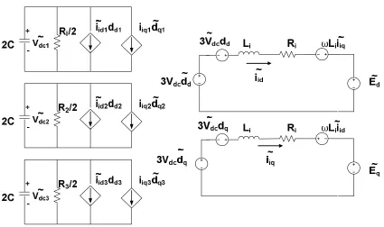
Figure 5.1 Input filter and rectifier representation of the SST. ...63
Figure 5.2 Power flow representation on the HVDC side. ...64
Figure 5.3 DAB repsentation in the average model. ...65
Figure 5.4 SST load inverter and filter implementation. ...67
Figure 5.5 SST local load inverter control. ...68
Figure 5.6 DQ to abc frame implementation ... Figure 5.7 Delta connection of the Substation SSTs. ...71
Figure 5.8 SST Based Distribution System. ...74
Figure 5.9 Start-up of the load SST with storage using switching models. Alignment of the grid and the SST output voltages is shown and the consequent grid connection at 0.2sec can be observed. ...76
Figure 5.10 700 kVA Load SST input voltage & current. ...78
Figure 5.11 700 kVA Load SST Input Real & Reactive Power. ...78
Figure 5.12 Substation SST Output Voltage & Current. ...79
Figure 5.13 400kVA Load SST Input Voltage & Current. ...79
Figure 5.14 700 kVA Load SST input voltage & current. ...80
Figure 5.15 700 kVA Load SST Input Real & Reactive Power. ...80
ix
Figure 5.17 Load SST sustaining its functionality under fault. ...82
Figure 5.18 Load SST Protection disconnecting the SST from the grid. (Top) HVDC bus Voltage. ...83
Figure 5.19 The Substation SST restricting the fault current to 2 pu...83
Figure 5.20H VDC bus surging during fault. ...84
Figure 5.21 SST’s response to grid side fault in Mode 1. ...86
x
LIST OF TABLES
Table 2.1 Switching Table ...8Table 4.1 Mode 3 Logic for Master and Slave. ...47
Table 4.2 Mode 2 logic for Master and Slave. ...48
1
1
INTRODUCTION
The initial idea of the Solid State Transformer (SST) was conceptualized with the vision of
offsetting the drawbacks of the conventional transformers such as the large size and
weight, voltage drop under load, sensitivity to harmonics, no energy storage etc. Utilizing
the SST topology put forth in [1], successfully mitigates these drawbacks while leaving room
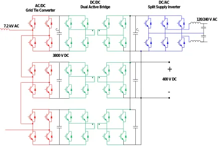
to incorporate plenty more features to it. A schematic of the topology for the SST is shown
in the figure below.
Figure 1.1 Solid State Transformer Topology
120/240 V AC DC/AC
Split Supply Inverter DC/DC
Dual Active Bridge AC/DC
Grid Tie Converter
CL CH
7.2 kV AC
400 V DC
+
2 The SST comprises of a grid tie voltage source converter, a bidirectional dc-dc converter
implemented as the Dual Active Bridge and a local voltage source inverter feeding the local
load. The distributed renewable energy resources and the distributed energy storage
devices can be directly connected to the LVDC bus of the SST.
One of the key features of the SST is the reduction in the size and weight with the current
topology. Studies show that the reduction can be 3times. If just an inductor is used as a
filter at the input of the SST this advantage may be lost or at least it is diminished. The
inductor rating, its size and weight increases as the power rating increases. A LCL filter
provides better filtering characteristics with lower inductance [2], thereby ensuring the
advantages of lower size and weight. However the increased order of the filter may
introduce stability issues. Methods to mitigate these issues have been discussed in Chapter
3.
In addition to the advantages stated earlier the SST can be controlled to operate under
different modes and thereby offering greater flexibility. This thesis focuses on these modes
of operation of the SST, from the SST point of view as well as from the power system point
of view.
Since the SST is being proposed as an alternative to the traditional transformer an obvious
mode is the rectifier mode of operation allowing voltage step-down operation as has been
discussed in previous works. In addition, the electric utility grid is being challenged by
3 Power electronics equipment is being used to address both of these challenges. The Solid
State Transformer system can incorporate value added functions for utility grid support and
to realize smart grid economic advantages in the presence of distributed resources, proper
communications and control structures. Depending on the nature of the line impedance
reactive power or real power compensation is required to provide voltage support. The SST
can be controlled to provide reactive and/or real power to the grid as per a set reference.
In addition, the SSTs can also be set up to operate in isolation from the grid i.e. in the
islanded mode. This mode of operation is also referred to as Black Start. Previous work [3]
also focused on the Black Start mode of operation for the SST through the droop method. In
the presence of communication however, the master-slave way of paralleling the SSTs
delivers better results.
An average model for the SST based on [1] has also been developed to enable system level
studies under these modes of operation. This model has been fine-tuned from the work
presented previously, to include realistic ride through capabilities and dynamics. A
hypothetical substation SST has been presented to enable a purely SST based system study.
The ability of the SST, a controlled device to control its output under severe faults and to
continue its operation even under fault presents an interesting case study. Moreover,
running the system level simulation helps identify the SST protection parameters and aids
4 Chapter 2 derives the small signal models for the different stages within the SST. Also design
and selection of components for the SST is discussed herein. Chapter 3 discusses different
modes of operation for the SST. The algorithms to determine the mode of operation for the
SSTs are also discussed. Chapter 4 includes results for the different operating modes of the
SST while also highlighting transition between these states. Chapter 5 discusses the average
modeling approach for the SST and also contains results for a test case demonstrating the
5
2
MODELING & DESIGN OF THE SOLID STATE TRANSFORMER
Further work in this thesis employs SSTs having different voltage ratings as well as
different power ratings. Even if the controls implemented are per unitized and the control
structure across these models are the same, owing to the varied power and voltage ratings
the component values of the system tend to vary. As a result controller tuning has been a
recurring component throughout this work. Developing a small signal model for the SST as a
result becomes imperative to facilitate controller tuning rather than attempting to manually
tune the controller at each step.
The switching model simulation is developed to emulate the hardware setup
available. As a result the grid frequency for this set of simulations is set at 60 Hz while the
single phase rms grid voltage is 120V. The HVDC as well as the LVDC bus voltages are set at
100V each while the local load voltage is regulated at 50V rms. The intermediate dual active
bridge employs a high frequency transformer with a 1:1 turns ratio. This SST is rated for
1kW. On the other hand the SSTs in the average model are of two types; the load SST and
the Substation SST. The substation SST which is only a hypothetical implementation, if
considered as a black box acts simply as a step down transformer stepping down from 69 kV
to 7.2kV. The intermediate HVDC and LVDC voltage levels are 60kV and 15kV respectively
and the DAB transformer has a 4:1 turns ratio. The load SSTs on the other hand function as
bidirectional SSTs with the grid side voltage at 7.2kV and the load side voltage at 120V. The
6 having the corresponding turns ratio. A diagrammatic representation of the different SSTs is
shown in fig 2.1.
7 2.1 SST Modeling:
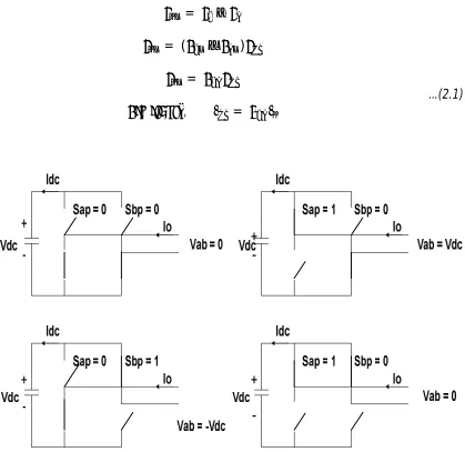
The grid tie converter has a cascaded H-bridge structure and can be employed as a boost
rectifier or as a voltage source inverter. For a voltage source converter (VSC) with a single H
bridge structure the possible switching combinations and the resulting currents and
voltages are shown in fig 2.2 and tabulated in table 2.1.
= −
= ( − )
=
, =
…(2.1)
8 Table 2.1 Switching Table
Sap Sbp Vop Idc
0 0 0 0
0 1 - Vdc -Io
1 0 Vdc IO
1 1 0 0
A two port representation of the H-bridge VSC is as shown in fig 2.3.
Figure 2.3 Two port network for the H-Bridge.
Extending the 2 port network for a cascaded H- Bridge the network can be viewed as shown
in fig 2.4.
Consequently,
9
ℎ : = 1 ( )
ℎ − : = = 1−
ℎ , = 1 ( ) = −
, = 1 ( ) =
ℎ , = …(2.2)
To simplify the average model it may be assumed that all dc voltages and duty cycles of
each are equal i.e. Vdc1 = Vdc2 = …. =Vdcn and dai = da, dbi =db ,…,dni = dn.
10
2.1.1 Grid Tie Converter Average Model:
a. Grid Tie Rectifier Model:
Consider the boost rectifier circuit with a LCL filter as shown in fig 2.5
11 Employing Kirchhoff’s voltage and current laws :
= 3 − −
= −
= − −
=− − …(2.3)
Since it is a single phase circuit to solve for the dq space we create an orthogonal circuit .
The equations for which are :
= 3 − −
= −
= − −
=− − …(2.4)
If the 120 Hz ripple [1] on the DC capacitor is neglected then Vm = Vdc. The above equations
12
= 3 − −
= −
= − −
2 =−
−2 …(2.5)
Here,
= , = , = , =
…(2.6)
Using the single phase d-q transformation:
= .
= sin ( ) −cos ( )
cos( ) sin ( ) ℎ , = 2
= .
. = 0 −
0
….(2.7)
13
= 3 − − −
= − − 0 −0
= − − −
2 = −[ ] −2 …(2.8)
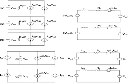
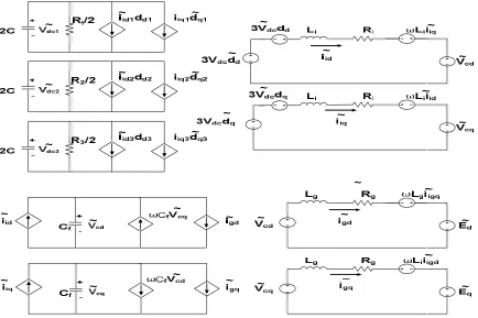
The average model of the grid tie rectifier in the dq frame is shown in Fig 2.6.
14 The small signal model for the Grid tie Rectifier can be obtained from these equations by
first determining a quiescent point and then applying a small perturbation to all the system
inputs.
̃
̃ = 3 + 3 −
− ̃
̃ −
= ̃̃ − ̃
̃ −
0 −
0
̃
̃ = −
− ̃
̃ −
2 = − −[ ] ̃
̃ −
2 …(2.9)
15 Figure 2.7 Small Signal Model for the Grid Tie Rectifier in the d-q frame.
For SSTs with just the L-filter in place of the LCL the analysis is simplified and the equations
are given as:
̃
̃ = 3 + 3 −
− ̃
̃ −
2 = − −[ ] ̃
̃ −
16 Figure 2.8 Small Signal Model for the Grid Tie Rectifier with L-filter in the d-q frame.
b. Standalone Inverter Average Model:
In the inverter mode the DC bus is assumed to stay constant. For the grid tie inverter
mode the small signal model derivation stays consistent with the method adopted in
the previous section. The 4th equation in the set of equations in 2.9 may be then
dropped.
The standalone converter is responsible to regulate the line voltage within specified
limits, since the grid is no longer available in this mode of operation. This analysis
extends to both the cascaded-H bridge converter in the standalone inverter mode as
well as to the local load inverter. Approximating a resistive load as in fig 2.1, the
17
= 3 − − −
= − − 0 −0
= − + −
+
…(2.11)
Consequently, the small signal model equations may be written as,
̃
̃ = 3 + 3 −
− ̃ ̃ − = ̃̃ − ̃ ̃ − 0 − 0 ̃ ̃ = − + − + ̃ ̃ …(2.12)
From the above set of equations it can be seen that in the standalone mode of operation,
the grid current and consequently the capacitor voltage is directly impacted by the load
variations, as such the controller should have a large enough bandwidth to regulate the
18 Figure 2.9 Small Signal Model For the Standalone Inverter in the d-q frame
The control modes for the grid tie converter have been discussed in greater detail in
chapter 3.
2.2 Dual Active Bridge (DAB) Average Modeling:
The DAB is an isolated, buck and boost dc-dc converter [4]. The basic DAB structure
is shown in fig 2.10.
19 The dc-dc DAB can be controlled by introducing a phase shift between the two H-bridges or
by varying the duty cycle of the switches or by varying the frequency of switching. The
implementation in this work employs a dc-dc DAB switching at a fixed frequency and duty
cycle while varying the phase difference between the two H-bridges. In the high frequency
transformer, the leakage inductance of the transformer provides energy and storage, while
the magnetizing inductance should be designed so as to have minimum impact on the DAB
operation. Assuming the DAB is operating with a delay of dDAB between the two bridges,
during the time 0<t< dDAB *T the current in the leakage inductance (Il) builds up. During the
time dDAB *T<t<T/2, the current stays more or less at the same value and during the time
T/2<t<T/2+ dDAB *T the current ramps down and so on as shown in fig 2.11
20 The power flow equation for the DAB is as shown in 2.13. Here, L is the leakage inductance
and n = n1/n2.
= ∗
2 (1− )
.…( 2.13)
The average model for the DAB is given in Fig 2.12
Figure 2.12 Average Model of the Dual Active Bridge (DAB).
=
2 (1− )
…(2.14) The high frequency transformer is an important aspect of the dual active bridge. Within the
HF transformer the leakage inductor forms the critical energy storage and power transfer
component, while the magnetizing inductance is desired to have minimal effect on the DAB
operation. The value of this leakage inductance can be computed from the formula in 2.13.
The maximum delay dDC is designed to be 1/4th of the switching period Tsw. Hence, rewriting
21
= ∗
2 (1− )
…(2.15)
2.2.1 DAB Control:
The dual active bridge can transfer power in either direction. The mode of operation of the
DAB in turn depends on the mode of operation of the Solid State Transformer as such.
While the SST is supplying power to the grid, the DAB functions to regulate the HVDC bus.
Since the SST topology employs three DABs operating in parallel we have one control loop
for each of the DABs. In this mode, the control structure employs a simple voltage feedback,
being compared with a reference and then being fed to a PI compensator. The output of
this compensator is the delay for the DAB operation.
During the time the SST draws power from the grid the three parallel DABs function to
regulate the common LVDC bus. As a result to maintain balance between the HVDC buses,
the power imbalance between the DABs need to be minimized. To achieve this, a dual loop
structure is adopted. A common outer voltage loop feeds the error in the LVDC bus voltage
to a PI controller which outputs the reference current. The DAB primary current is then
22
*
Vref
VHDC
DC d *
Vref
VLDC
ireft
ireft
iref
iref
iprimary
1
ddc
Figure 2.13 Control loops for the DAB
Also in this mode of operations the three DABs are interleaved i.e. the carriers are time
shifted (120 degrees) with respect to each other. As a result with 3 DABs in parallel the
switching ripple is now thrice the switching frequency and the DC voltage is much cleaner.
Figure 2.14 Carrier Interleaving for the three DABs.
2.3 Solid State Transformer Design:
As it was stated in the previous section, SSTs with different ratings have been utilized
throughout this work. Hence a general frame work for component selection is established in
23 cascaded H-bridge structure which interfaces with the grid. A LCL filter is employed to
enable this grid interfacing. Internal to the SST connected to this converter is the HVDC bus.
Three DABs connect the HVDC bus to a LVDC bus which in turn feeds the local inverter. The
local inverter interface with the load is established through a LCL filter as well.
2.3.1 The LCL filter:
Before proceeding with the filter design it is required to determine the system base
values. The power base Sbase is the SST power rating while the voltage base Vbase is the same
as the grid voltage. The current and impedance base values can be determined as follows:
= & =
= 1 & = …(2.16)
References [5,6] state that
+ < 10%
And
< 5%
…(2.17)
Li is selected such that the THD of the current is restricted to 10 to 30%. Imposing further
stringent THD requirements at this stage would push the resonant frequency closer to the
switching frequency. Thereon, Lg is selected and simulations are run so as to ensure the THD
24 Figure 2.15 Current and THD(%) waveform with the LCL filter.
The grid tie converter, in the rectifier mode functions as a boost rectifier. The modulation
index is given as in 2.18, where Vp is the peak grid voltage value while VLVDC is the LVDC bus
voltage.
=
…(2.18)Higher DC bus voltage facilitates lower input current THD and better reactive power flow
control [1]. In order to determine the value of the capacitor, storage ability is chosen to be
the determining factor. The capacitor is designed so as to permit 17msec ride through
capability. This is an important design parameter. The equation for capacitor design is given
below:
1
25
3
OPERATING MODES OF THE SOLID STATE TRANSFORMER
The solid state transformer structure and modeling were discussed in the previous chapter.
Depending on the grid conditions, the status of the available distributed energy resources
and the local load requirement, the same SST unit can push power into the grid or draw
power from the grid simply by varying the references and control structures. A supervisory
control that makes decisions based on the grid availability, available energy from the
distributed energy resources and the local load power requirement can be employed to
vary the mode of operation.
3.1 The Rectifier Mode of Operation
This is the conventional mode of SST operation. The operating state of the SST can be
described as follows. The grid is available and power needs to be drawn in from the grid to
supply the local load of the SST, since the power available from the distributed resources is
less than the local load requirement. In this mode the grid tie converter operates in the
rectifier mode and controls the HVDC bus voltage. The DAB regulates the LVDC bus voltage
while the local inverter feeds the local load. The direction of power flow under this mode is
shown in fig 3.1. Control design for the grid tie converter under different modes of
operation shall be further addressed through this chapter.
The control structure for the rectifier is a dual loop structure. In comparison with the dual
loop structure employed in [1] the control structure under consideration has to account for
26 Hence before designing the controller it is required to obtain the transfer function between
the converter voltage and current. To do so consider the block diagram as shown in fig 3.2,
Figure 3.1 Power Flow during the Rectifier mode of operation.(SST Simplified)
Figure 3.2 LCL structure with the SST sourcing power from the grid.
The block diagram above [5] does not consider the effective series resistance (ESR) with the
inductors and capacitors.
Split Supply Inverter Dual Active Bridge Grid Tie Converter CL CH
PSST PDAB PLOCAL
DRER/DESD PDRER/DESD 1 sLg 1 sC 1 sLi V(s) E(s) I(s)
Ic(s)
27
( ) = ( )
( )=
1 ( + )
( + )
…(3.1)
In the rectifier mode of operation with the grid sourcing power from the grid, the plant and
controller block diagram is as shown in fig. 3. The inner loop regulates the inverter side
inductor current while the outer loop regulates the DC bus voltage as shown in fig 3.3.
Figure 3.3 Control Structure for the grid tie converter in the rectifier mode of operation.
Since all the controls are being implemented in the d-q frame, the PI controllers assure
good tracking of the reference. To suppress the 120 Hz ripple on the DC bus the bandwidth
of the inner and outer control loops are designed at 70 and 4 Hz respectively. However
because of the higher order system the inner loop with just the PI compensator is unstable.
The system may be stabilized by means of damping which may be either active or passive.
Passive damping involves addition of physical resistors in series with the filter inductances
and the capacitors to damp the resonance of the filter. This though, tends to reduce system
efficiency. A more efficient way of damping the system is by means of active damping.
Active damping may be implemented by compensating the system with filters or by
employing multiple loops thereby requiring more number of sensors. In the control
Gc(s) ERL
2Vdc(sCRL+1)
Gpwm(s)
PI PI
Vdcref V
dc
I(s)
I*(s) U(s)
28 structures employed in this work, the cascaded filter method of compensation is employed.
Notch, high pass, or low pass filters may be used depending on the application and user
preference. A simple low pass filter with the cut off frequency at 200 Hz is employed in this
case, due to ease of implementation in practical scenarios [7,8,9]. The transfer function of a
simple low pass filters as shown:
( ) =
+ …(3.2)
Where ωc = 2*pi*200. The modified block diagram of the control structure is shown in fig
3.4.
Figure 3.4 Modified block diagram of the control structure with active damping filter included.
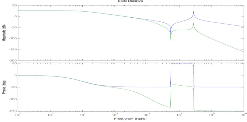
The frequency response of the compensated system with and without active damping is as
29 Figure 3.5 Bode Plot for the compensated inner loop with (Green) and without (Blue) the
active damping filter.
30 The frequency response of the outer loop of the compensated system is as shown below:
Figure 3.7 Bode plot for the outer loop showing the phase and gain margins.
3.2 The Grid Tie Inverter Mode of Operation:
The SST is designed to be an intelligent energy router device. In addition, to enabling
integration of renewables it can also provide value added functions like voltage and
frequency support which can be enabled by storage. To accommodate such functions the
SST should be able to drive power to the grid whenever such a request is raised.
The operating state of the SST can be described as follows. The grid is available and power
needs to be supplied in order to support the grid. In presence of storage in addition to the
31 power demands from the grid. In this mode, the grid tie converter operates in the inverter
mode and controls the power output to the grid. The DAB regulates the HVDC bus voltage
while the local inverter feeds the local load and the LVDC bus is regulated by a DC-DC
converter connected to the distributed resources (not shown). The direction of power flow
under this mode is shown in fig 3.8.
Figure 3.8 Power Flow during the Grid Tie Inverter mode of operation.
From a given real and reactive power reference the current reference can be obtained
using the following formulas
= ∗ − ∗
= ∗ + ∗ ...(3.3)
We have two equations and two unknowns and the current references can easily be
computed using the above two equations. A popular control structure employed involves
Split Supply Inverter Dual Active Bridge (DAB) CL CH DRER/DESD Grid Tie Converter
PSST PDAB PLOCAL
32 regulating the inverter output current against a set reference. However, with such a
topology it is seen that the grid voltage serves as interference to the system. To counter-act
this, the loop gain is intentionally designed to be extremely high. This however may not
guarantee suppression of this disturbance. In spite of this shortcoming, this scheme
provides good stability, dynamic response and facilitates simple controller design. To
counteract the grid voltage disturbance, the control strategy used involves an additional
outer current loop regulating the grid current [10]. The block diagram for this control
structure is shown in the figure below.
Figure 3.9 Control Structure for the grid tie Inverter.
While designing the inner control loop, Vc is assumed to be a disturbance. The simple pole
zero cancellation method with a gain to obtain the desired bandwidth is adopted. Again a
low pass filter (LPF) is employed to enable active damping. The bode plot for the inner loop
33 Figure 3.10 Bode Plot for the compensated inner current loop in the Grid Tie Inverter Mode
The bandwidth of the inner loop as can be seen is set to be at 1500 Hz. The PI compensator
is of the form,
( ) = ∗( + ) …(3.4)
As a result the closed loop transfer function of the inner loop is of the form,
( ) = +
…(3.5)
This transfer function is identical to the transfer function of a low pass filter seen in the
previous section. To ensure adequate damping an additional low pass filter at a frequency
34 at higher frequencies is incorporated. The outer loop cut off frequency is designed to be at
300 Hz. The outer loop with the compensator is shown in fig 3.10.
Figure 3.11 Bode plot for the compensated outer loop.
3.3 Standalone Inverter Mode of Operation:
In case of a grid failure, in the presence of adequate power available from the distributed
resources, the SSTs can be operated in parallel so as to restore supply to the local loads. The
SSTs can be operated in parallel using the droop mode of operation or using the
Master-Slave concept. In the absence of intelligent devices, the droop mode of operation presents a
suitable option. However, provided the SSTs are intelligent devices the Master-Slave
35 results for the two methods are compared in the following chapter. The Master SST,
preferably with the largest distributed resources would typically act as the Master. Of the
remaining SSTs, the ones with local generation and storage greater than the local load
requirement are capable of pushing power back into the grid, while the ones with local load
requirements greater than the local generation behave as loads. Drawing an analogy with
the Power System, the Master SST may be looked at as the slack bus, the other SSTs
supplying power can be compared to the PQ bus while the load SST is similar to the load
bus.
It is only the Master SST that needs to operate in the Standalone Inverter mode while the
other generating SSTs operate in the grid tie inverter mode and the load SSTs operate in the
rectifier mode [11]. In a real world scenario the available reserve power will not always be
sufficient to match the load requirements and it may be required to prioritize loads and
consequently resort to selective load shedding. This study however assumes sufficient
reserve power such that no load shedding measures are required. The sequence of events is
as shown in fig 3.11. In case of a fault in the system, breakers 2, 3, 4 need to be tripped to
prevent abnormal voltages appearing across the filter inductors. Breaker 1 trips to isolate
the system from the grid. This stage is shown in scenario 1. Hereafter the Master SST turns
36
MASTER SST PLOCAL< PDRER/DESD
SLAVE SST PLOCAL< PDRER/DESD
LOAD SST PLOCAL> PDRER/DESD
BRK1 PGRID = 0
PMASTER = 0
PSLAVE= 0
PLOAD= 0
MASTER SST PLOCAL< PDRER/DESD
SLAVE SST PLOCAL< PDRER/DESD
LOAD SST PLOCAL> PDRER/DESD
BRK1 PGRID = 0
PMASTER = 0
PSLAVE= 0
PLOAD= 0
MASTER SST PLOCAL< PDRER/DESD
SLAVE SST PLOCAL< PDRER/DESD
LOAD SST PLOCAL> PDRER/DESD
BRK1 PGRID = 0
PMASTER = 0
PSLAVE= 0
PLOAD= 0
MASTER SST PLOCAL< PDRER/DESD
SLAVE SST PLOCAL< PDRER/DESD
LOAD SST PLOCAL> PDRER/DESD
BRK1 PGRID = 0
PMASTER > 0
PSLAVE> 0
PLOAD< 0
1
3
2
4
BRK2 BRK3 BRK4 BRK2 BRK2 BRK2 BRK3 BRK3 BRK3 BRK4 BRK4 BRK41: Connection to the grid is lost and all SSTs are disconnected from the grid. (All breakers open [red] ).
2: Grid is still disconnected(BRK1 open). Master SST connects to the grid and establishes a voltage. (BRK2 closes [green]).
3: Grid is still disconnected(BRK1 open). Slave SST connects to the grid using the Master output voltage as reference and regulates its power to a zero reference. (BRK3 closes)
4: Grid is still disconnected(BRK1 open). Load SST connects and draws power jointly supplied by the Master and Slave SSTs. (BRK4 closes).
37 other SSTs is made available. The phase lock loop (PLL) for the other SSTs now use this
voltage set by the Master SST as the reference. The slave SSTs operate with Pref and Qref
set to 0 as shown in scenario 3. Thereafter, the load SSTs are introduced. In any case, after
the event of the grid connect breakers opening, all the SSTs enter the standalone mode
before proceeding on to operate in the grid tie inverter or rectifier mode [12].
In the standalone inverter mode, the Master SST is required to regulate the line voltage
within appropriate limits. The control structure again employs a dual loop topology with an
inverter current inner loop and a voltage outer loop. The current loop bandwidth is
designed to be much greater than the voltage loop bandwidth [13]. As a result the inner
current loop is able to track the current reference set by the outer loop very closely and
quickly and the inner current loop dynamics do not affect the outer voltage loop i.e. the
inner loop may be observed as just a gain. A block diagram of the control structure is shown
below:
Figure 3.13 Control Structure for the Standalone Inverter.
Gpwm 1
sLi+Ri
sCRd+1
sC
1 sLg+Rg
+ -Vab(s)
+ iLi(s)
vC(s) iLg(s)
-iC(s)
E(s)
PI LPF
38
While designing the inner control loop, Vc is assumed to be a disturbance. The simple pole
zero cancellation method with a gain to obtain the desired bandwidth is adopted. Again a
low pass filter (LPF) is employed to enable active damping. The bode plot for the inner loop
is shown in fig 3.13. The inner loop bandwidth is again set at 1500Hz. The outer voltage loop
regulates the filter capacitor voltage. The reference for this voltage is set internally.
39 Figure 3.15 Bode Plot for the compensated outer current loop in the Standalone Inverter
Mode.
3.4 Dual Active Bridge Modes:
The dual active bridge as covered in chapter 2 can permit power flow in either direction.
During Modes 2 & 3 of operation the three DABs operating in parallel charge the respective
LVDC buses, pushing out power from the distributed resources available to the grid. During
Mode 1 of operation the three parallel DABs are used to charge the HVDC bus. In this mode
in addition to regulating the HVDC bus, balanced current sharing has to be ensured
between the three DABs [1]. To do so the loop regulating the HVDC bus is used to generate
the current reference while an inner current loop assures proper current sharing. The
imbalance may be caused by a variety of factors from system parasitic components to
different leakage impedances of the high frequency transformers. Mode changes in the DAB
occur simultaneously with the grid tie converter. The control structures for the two modes
40 3.5 Supervisory Control for the Solid State Transformer:
While developing the modes of operation for the SST, it is required to classify the SSTs into
2 main categories, namely the Master SST and the others. The sequence of operations for
both classes of SSTs are described in figures 3.14 and 3.15 respectively. Mode1 in the
schematic is used to refer to the rectifier mode of operation, Mode 2 to the grid tie inverter
mode of operation while Mode 3 to the standalone mode of operation. Also shown are the
parameters used to enable the internal protection of the SST.
3.5.1.1Supervisory Control for the Master SST:
To implement soft start of the SST it is required that the SST has some reserve storage
during start up. At start up the HVDC bus is charged through the DAB. Once, the HVDC bus
voltage crosses a threshold, the SST checks for the availability of the grid. If the availability
of the grid is detected, the PLL is activated and the SST begins operating in Mode 3
regulating its output voltage to align with the grid voltage. Once the two vectors are aligned
the breaker connecting the SST to the grid is closed. Following which the SST enters Mode1
of operation and starts supplying the load. In cases where the reserve power available from
the distributed resources and the storage combined exceeds the required local load
demand, the SST may start injecting power back in the grid. This may be permissible when
there is a requirement from the grid to be supported from these distributed resources or in
cases where the power being generated from the renewables cannot be stored in the
41
SST Turn “ON”
DRER/DESD Charges the LV Bus of the SST.
DAB switches to charge the HV bus of the SST
Grid Available
Activate PLL & start synchronizing with Grid.
Generate internal reference
Operate in “MODE 3” Close Breaker
Operate in “Mode 1” DESR+DESD > Load
Operate in “Mode 2” Pref/Qref > 0 Or Storage full
Operate in “MODE 3”
N
O
YE
S
YESYE
S
NOGrid Status High to Low
DC Bus Surge or Droop
Open Breaker Close Breaker YES 1 1 NO
Stop Switching -> Zero State
YES
Open Breaker
42 If such is the case then Mode 2 operation commences. While transiting from Mode 1 to
Mode 2 it is required to ramp the current reference down to zero and then shift modes. If
not implemented undesired transients may be observed in the currents as well as voltage
and in some cases damaging the SST components. Even while operating in Mode 2 the
constraint for DESR+DESD>Load is constantly monitored. As this difference reduces and falls
below a certain threshold the SST reverts back to operation in Mode1.
In the case where the grid is unavailable, the Master SST enters Mode 3 and regulates the
line voltage in accordance with an internally generated reference. While in this mode the
grid availability is constantly tracked. If the grid becomes available, the reference is to be
gradually set to be the grid voltage by steadily reducing the phase shift existing between the
internally generated reference and the grid vector. Once this is done the connection with
the grid might be reestablished by closing Breaker 1 (fig 3.11) thereby connecting the
43
SST Turn “ON”
DRER/DESD Charges the LV Bus of the SST.
DAB switches to charge the HV bus of the SST
Grid Available
Activate PLL & start synchronizing
with Grid. Operate in “MODE 3” Close Breaker
Operate in “Mode 1” DESR+DESD > Load
Operate in “Mode 2” Pref/Qref > 0 Or Storage full
NO
YE
S
YESYE
S
NOGrid Status High to Low
DC Bus Surge or Droop
Open Breaker
YES 1
1
NO
Stop Switching -> Zero State
YES
Open Breaker
44 During every computing cycle it is also important to continuously monitor the availability of
grid voltage. In case of a total outage, the breaker connecting the SST to the rest of the
network is opened and kept in a stand-by mode to prepare for the Black Start operation. In
case of the DC bus voltages violating permissible boundaries of operation, the SST is
disconnected from the network and all the converters are put to the zero switching state to
prevent any damage to its components.
3.5.1.2Supervisory Control for the Slave SST:
For the SSTs which are not expected to behave as the Master in standalone conditions, the
sequence of operations is simply denoted by the first chain of events as described for the
Master SST. If no voltage is detected at its input, these SSTs are expected to stay in the
standby mode until the Master SST can establish a voltage. Here on, the SSTs introduced to
45
4
SWITCHING SIMULATION RESULTS
4.1 The D-Q Controller for SST:
The average models in the dq frame for the grid tie converter as well as for the local
inverter were derived in chapter 2. The grid tie converter average models for both the grid
tie mode of operation as well as the stand alone modes were derived. Chapter 3 deals with
different control modes of operation for the SST and also focused on different control
structures for the SST. This chapter will highlight implementation and results of the
switching model simulation.
The controls for the different modes for the grid tie converter i.e. the rectifier mode
the grid tie inverter mode and standalone inverter modes are all been implemented in the
d-q frame. Looking at the average models derived in chapter 3 coupling between the d and
q networks can be observed. In order to control the d-q parameters independently,
decoupling terms are included in the control structure. The control implementation for the
47 4.2 SST Logic Implementation:
The availability of the grid is determined by the status of the breaker BRK1 in the
figure below. Mode 3 as explained in Chapter 3 is applicable for all the SSTs during start-up.
For the slave SSTs Mode 3 is applicable during start-up only.
Table 4.1 Mode 3 Logic for Master and Slave.
MODE 3
Master Slave
Vgrid Vgrid (del) Logic Vgrid Vgrid (del) Logic
0 0 1 0 0 0
0 1 1 0 1 1
1 0 1 1 0 1
1 1 0 1 1 0
When the connection to the grid is reestablished, the SST continues to operate in Mode 3
working to realign the converter output voltage with the grid voltage vector and bringing
down the grid current to zero before moving into Mode 1 or 2.
For the SST to operate in Mode 2, the first required condition is for the grid to be available.
Also, the available energy resources should be greater than the local load requirement.
48 Table 4.2 Mode 2 logic for Master and Slave.
MODE 2 (Slave)
Vgrid Vgrid(del) BRK4 Mode 3 PC GPR Logic
1 0 x X x x 0
1 1 0 X x x 0
1 1 1 X 0 x 0
1 1 1 X 1 0 0
1 1 1 X 1 1 1
0 1 x X x x 0
0 0 0 X x x 0
0 0 1 0 1 0 0
0 0 1 0 1 1 0
0 0 1 1 x x 0
PC: Power Constraint (P(Energy Resources) > P(local Load) GPR: Grid Power Request
GC: Grid Connection LL: Local Load Connected
From the above table it can be inferred that post start-up the SST would always need to
enter Mode 1. Since the SST can operate in Mode 2 only once the power constraint is met,
this is required. In case the power constraint is not met, irrespective of the grid requirement
49 connection is steadily established, it is self-sufficient in supplying the local load and there is
a requirement from the grid to supply power. Again, when moving from Mode 2 to Mode 1
in the presence of the grid, the grid current needs to be ramped down to zero in a
controlled fashion, before switching modes.
For Mode1 operation, it then becomes a case of exclusivity. In case the grid is established
and the Vgrid (delay) is true and the SST is operating neither in Mode 2 or Mode 3, Mode 1
is the selected mode of operation.
Table 4.3 Mode 1 logic.
MODE1
Vgrid Vgrid(del) Mode 2 Mode 3 Logic
0 X x x 0
0 1 x x 0
1 0 x x 0
1 0 x x 0
1 1 1 x 0
1 1 0 1 0
50 4.3 SST Start – Up:
It is not advisable to start switching the grid tie converter even as the HVDC bus
voltages are zero. Doing so will lead to large input inrush currents which may damage the
switches or other components of the network. In the absence of storage, typically the grid
tie converter is allowed to operate as a full bridge rectifier and the HVDC bus is allowed to
charge to the peak value of the grid voltage minus the voltage drop along the line. Even as
such, large current spikes are observed but, it is the diodes and not the IGBT switches that
conduct these currents. In the presence of storage however, the SST may be operated in
Mode 3 with the grid tie converter operating as a standalone inverter and using the grid
voltage itself as its reference. Once the grid voltage vector aligns with the grid voltage
vector, then connection with the grid may be established. In such a case no current spike is
51 Figure 4.2 Soft Start for the SST.
4.4 Mode 1: Rectifier Operation:
The SST behavior in this mode of operation has already been discussed in chapter 3.
In the simulation case under study, the SST enters Mode I of operation after start up. During
start up, the SST is operating in Mode 3. The transition from Mode 3 to Mode 1 is not
instantaneous. The current reference should be ramped down to zero i.e. the converter
output voltage vector and the grid voltage vectors should be exactly aligned. Since in the
start-up mode this is already ensured the transition can be readily made. At 0.6 secs the SST
DAB charging up the LVDC
bus. Grid Connection Established at
0.4sec
Mode 1 Operation
52 enters Mode 1 of operation. The steps of operation during start-up followed by the SST
entering Mode 1:
1. Following the closure of BRK1, BRK3 closes connecting the HVDC bus to the
distributed energy resources.
2. The DAB starts switching to charge the LVDC bus.
3. Simultaneously, the grid tie converter starts operating in the stand alone mode
regulating the converter output voltage to align it with the grid voltage vector.
4. Once the vectors are aligned BRK2 is closed to establish grid connection (0.3 sec).
5. The converter continues to operate in the standalone inverter mode, regulating the
output current to zero.
6. Hereafter, the SST shifts to Mode 1 operation (0.5sec).
7. Simultaneously, the DAB starts regulating the HVDC bus & the load is connected.
53 4.5 Mode 2: Grid Tie Inverter Operation:
In Mode 2 it is assumed the grid provides the reference required to drive power out of the
SST. Once the transition from Mode 1 to Mode 2 is made, the power reference gets ramped
up from 0 to the required value (assuming availability of resources). During this transition
the following sequence of events take place.
1. Once the reference is set by the grid and the Power Constraint requirement has
been verified, the Mode2Active signal is set.
2. Following this, the DAB begins to regulate the LVDC bus and the grid current
reference is ramped down to zero.
3. Post this, the SST shifts to Mode 2. At this point it is important to keep the
modulation index the same as the previous instant. If not the system might see
undesirable current peaks.
4. Once the grid tie inverter operation begins the current reference is ramped up from
54 Figure 4.4 Termination of Rectifier mode of operation of the SST.
Figure 4.5 Waveforms for Grid-Tie Inverter Mode of Operation (Grid Current , LVDC ).
Mode1 Operation terminates at
1.5 sec. Current reference gets
ramped down and the DAB
starts controlling the
55 4.6 Mode 3: Black Start Operation:
To simulate Mode 3 of operation, BRK1 is opened indicating non availability of the grid. In
such a case all the SSTs satisfying the power constraint requirement enter Mode 3 while
those that are unable to meet the requirement shed the connected load and then enter
Mode 3. The network is to stay in this state for 0.5 secs to permit reconnection to the grid.
If the connection to the grid is not established the Master connects to the network, thereby
establishing the voltage. Sensing the restoration of voltage the other Slave and Load SSTs
begin operating.
1. Upon loosing connection to the grid, all the SSTs are disconnected from the grid.
2. The Master SST enters Mode 3 of operation.
3. After a delay of 0.5 sec (permitting time for the fault to be cleared and reconnection
56 Figure 4.6 Disconnection of the SST from the grid.
In the absence of the grid, the SSTs operate in parallel in what is referred to as the black
start mode of operation. In order to enable parallel operation of the inverters, the
Master-Slave concept was employed. The sequence of events in the black start mode were
previously explained in section 3.3 and 3.5.
In the stand alone mode, ideally the control structure of choice would be to employ an
outer voltage loop followed by an inner capacitor current loop, which provides a stiff output
voltage against large load variations, employing minimum sensors. In this development
however, sensors measuring and feeding back the grid current are already employed for the
grid tie inverter mode of operation. Hence the control structure that employs an outer
Grid Connection
57 voltage loop and an inner inverter side inductor current loop with load current feedforward
ensuring the output voltage remains stiff, is employed [18,19].
The consequent Master SST output voltage waveform, with the load varying from 10% to
full rated load as a step is shown in the figure below.
Figure 4.7 Waveforms showing stiffness in the output voltage against load variations.
In the black start mode of operation, another alternative is to parallel all the SSTs online
through the droop control mode. In the droop control mode the inverters mimic the
operation of synchronous generators, whose output voltages and frequencies vary as a
function of the real and reactive power supplied and also depending on the nature of the
line impedance in order to ensure minimal mismatch in power sharing between generators.
58 always more resistive. In the switching simulations, the lines connecting the SSTs and the
loads are deemed to be largely resistive or with low .
Consider the circuit as shown in the figure below:
Figure 4.8 Power flow between two points.
The equations for the real and reactive power are given as:
=
+ [ ( − ) + ]
=
+ [ ( − )− ]
For a largely resistive line or a line with low
ratio,
if the inductance is ignored andtherefore assuming φ to be very small, from the equations it can be seen the need for both
P/V and Q/f droops [19,20].
To ensure good current sharing a virtual impedance is incorporated in the control loop to
ensure proper current sharing as well as to minimize circulating currents [21,22]. In this case
59 as the Droop method for paralleling the converters are shown. The line impedance values
are X1 = 1 microH and R1 = 0.75 ohm and X2 = 6 microH and R2 = 0.8 ohm.
In the presence of communication, the performance of the Master Slave approach is
preferable to that of the droop. The inclusion of the virtual impedance causes a drop in the
converter output voltage. Also for large differences in the line impedance that the virtual
impedance is not able to compensate for, large circulating currents are observed as a result
61 Figure 4.10 Voltage and Current Waveforms for two SSTs operating in the Standalone mode. (Left) The Master-Slave
62
5
SST AVERAGE MODEL SIMULATION
Solid State Transformers have been envisioned to eventually replace the huge oil/vacuum
transformers currently operating in the electric grids. To enable simulation of such a
system, made up of solid state transformers using simulation software such as Matlab,
PSCAD etc. requires the development of average models which are far less computationally
intensive when compared to their switching counterparts. Some of the effects which cannot
be directly translated from the switching to the average model include the switching ripple
originating from the toggling of the power devices, the common mode voltage, dc bus
imbalance effects etc. However the average model developed gives a fairly accurate
representation of how the actual switching model would behave under various test
conditions. The average model is not truly average in the real sense. Circuit & control
elements have been retained to effectively replicate transient responses of the SST.
Descriptions of the various SST stages along with component sizing & control selection have
been described in the following sections.
Average model of the SSTs have been developed [23,24] to facilitate such system level
studies. The average model employed in this study is based off the model described in [23]
and developed in PSCAD. This study focuses on modifying the existing models to better
match the switching model and demonstrating the model effectiveness through a system
63 5.1 Rectifier Stage:
As shown in the figure below the rectifier has been modeled as a controlled voltage source.
The inductor in series is the filter inductance which ties the SST to the grid. The inductor size
is restricted to be at 10% of the base inductance value. The controlled voltage source
control signal is a product of the modulating signal and the HVDC bus voltage (DC bus on
the high voltage side). The DC link capacitor sizing is done such that the system inertia is at
15ms (to enable modules to scale up satisfactorily).
Figure 5.1 Input filter and rectifier representation of the SST.
The control structure and power flow in and out of the SST rectifier stage are modeled as in
fig.
1 ∗ ℎ −
3∗ ℎ = ℎ
64 Here Vsigs*Ihs is the instantaneous input power, Pdcl is the power to the secondary of the
DAB & Vhdc is the voltage of the HVDC bus. The multiplier 3 is used since the switching
model would employ a 7 level cascaded structure with 3 DC capacitors. The ‘Soft Start’ or
the ‘Start Up’ of the SST has not been modeled. Rather modeling the capacitor as an
integrator enables us to reset the capacitor voltage to a desired value upon start up. The
control structure is the standard as used with the switching model with an outer voltage
loop regulating the DC bus voltage with a cut off frequency of 4Hz and an outer current loop
regulating the line current with a cut off frequency of 70 Hz as before.
65 5.2 Dual Active Bridge:
The dual active bridge is modeled in accordance to the equation below and is shown in Fig
5.3
= ∗ ℎ ∗
2∗ ∗ ∗ ∗(1− )
The LVDC bus is again designed such that the system inertia is 17msec.
0.5∗ ∗
= 0.017
Figure 5.3 DAB repsentation in the average model.
The output of the PI compensator gives the delay ‘d’. The model in fig 5.3 in terms of
66
= ∗ ℎ ∗
2∗ ∗ ∗ ∗(1− )− −
= ∗ + ∗
= ∗ + ∗
= 1 +
Where K is the value of the DC bus voltage at t<0 and Plosses and Pload correspond to the
power lost and power consumed on the load end.
5.3 Load Inverter:
As the system VA rating keeps increasing, the system current ratings increase as well. As a
result inductor size and weight increase as well. Hence LCL filter as against L/LC filters is a
better option. In addition in case of a fault on the load side, the additional inductance helps
restrict surge in the fault current owing to the capacitor discharge. Assuming a switching
frequency of 10kHz, the resonance of the LCL filter is designed to be under 5kHz. Again the
process adopted is:
a. Inverter side Inductance + Load Side Inductance < 10% system base inductance
b. Filter capacitance < 5% system base Capacitance
c. Resonant frequency =
67 The control loop consists of an outer voltage loop (cutoff frequency of about 300Hz)
regulating the capacitor voltage & an inner current loop (cutoff frequency of about 1500Hz)
regulating the inverter side current. In addition high pass filtering of the voltage is done so
as to ensure active damping of the LCL filter resonance.
68
69 5.4 D-Q to abc Transformation:
To ensure proper representation of the switching model it is required to restrict the
modulating signal to less than or equal to 1. At the same time saturating the signal will give
rise to undue harmonics in the current waveform. Hence the D-Q to abc transformation was
redone as shown in fig 5.5.
The absolute values of Vdd and Vqq are used to determine the amplitude and angle. The sign
of Vdd and Vqq are used to determine the sector and thereby arrive at the right modulating
signal. For example, in a scenario where Vdd = 0.9 and Vqq = -0.8 which may occur since the
controller restricts the absolute values of Vdd and Vqq between 1 and -1. In such a case the
implementation below will restrict the magnitude of the modulating signal to 1 while
preserving the appropriate phase difference with respect to the grid. This is important since
the average model simulates the resultant voltage as a product of the modulating signal and
the DC bus. In actuality depending on the PWM scheme adopted the maximum achievable
is restricted to under 1 (line to phase) for the VSC. Thus such a transformation ensures more
71 5.5 SST Average Model Behavior:
Two sets of average models for the SST have been developed; the Substation SST & the
Load SST. The Substation SST emulates a step down transformer & steps down the voltage
from 69kV (phase voltage) on its primary side to 7.2kV (phase voltage) on its secondary. The
Substation SST is rated for 7MVA & can be scaled from 3.5MVA to 10 MVA. The load SST
follows the concept of a distribution transformer and reduces the voltage from 7.2kV to
120V.