ND-70924 (E) ISSUE 1 STOCK # 151993
Data Interface System Manual
®
LIABILITY DISCLAIMER
NEC America, Inc. reserves the right to change the specifications, functions, or features, at any time, without notice.
NEC America, Inc. has prepared this document for use by its employees and customers. The information contained herein is the property of NEC America, Inc. and shall not be reproduced without prior written approval from NEC America, Inc.
NEAX and Dterm are registered trademarks of NEC Corporation. Copyright 2000
NEC America, Inc.
ISSUE 1 ISSUE 2 ISSUE 3 ISSUE 4
DATE JULY, 2000 DATE DATE DATE
ISSUE 5 ISSUE 6 ISSUE 7 ISSUE 8
DATE DATE DATE DATE
NEAX2000 IVS2
Data Interface System Manual Revision Sheet 1/2
ND-70924 (E) PAGE No.
ISSUE No.
1 2 3 4 5 6 7 8
i 1 ii 1 iii 1 iv 1 1 1 2 1 3 1 4 1 5 1 6 1 7 1 8 1 9 1 10 1 11 1 12 1 13 1 14 1 15 1 16 1 17 1 18 1 19 1 20 1 21 1 22 1 23 1 24 1 25 1 26 1 27 1 28 1 29 1 30 1 31 1 32 1 33 1 34 1 35 1 36 1 37 1 38 1 39 1 40 1 41 1 42 1 43 1 44 1 45 1 46 1 47 1 48 1 49 1 50 1 51 1 52 1 53 1 54 1 55 1 56 1 57 1 58 1 59 1 60 1 61 1 62 1 63 1 64 1 65 1 66 1 67 1 68 1 69 1 70 1 71 1 72 1 PAGE No. ISSUE No.
73 1
74 1
75 1
76 1
77 1
78 1
79 1
80 1
81 1
82 1
83 1
84 1
85 1
86 1
87 1
88 1
89 1
90 1
91 1
92 1
93 1
94 1
PAGE No.
ISSUE No.
1 2 3 4 5 6 7 8
PAGE No.
ISSUE No.
NEAX2000 IVS
2Data Interface System Manual
TABLE OF CONTENTS
Page
LIST OF FIGURES . . . iii
LIST OF TABLES . . . iv
INTRODUCTION . . . 1
PURPOSE . . . . . 1
OUTLINE OF THIS MANUAL . . . 1
REFERENCE MANUAL . . . 2
CHAPTER 1 GENERAL INFORMATION . . . 3
SYSTEM OUTLINE . . . 4
DPC . . . . . . . 7
DTI . . . . . . 7
M03 . . . . . . . 7
PLO . . . . . . . 8
CARD NAME AND FUNCTION . . . 9
SYSTEM CAPACITY . . . 11
System Capacity for Data Interface . . . 11
System Capacity for Digital Trunk Interface . . . 11
SYSTEM SPECIFICATIONS . . . 12
DPC Specifications . . . 12
Modem Specifications . . . . 12
SYSTEM CONDITIONS . . . 13
Time Slot Assignment Condition . . . 13
Time Slot Allocation for DTI Card . . . 14
CHAPTER 2 INSTALLATION . . . 15
PRECAUTIONS . . . 16
Static Electricity Guard . . . 16
REQUIRED EQUIPMENT . . . 19
INSTALLATION PROCEDURE FOR DATA INTERFACE . . . 20
Installation Summary for Data Interface . . . 20
Mounting DPC Card . . . . 21
Mounting M03 Card . . . . 21
Conditions on Connecting DTE . . . 22
Connecting X.21 DTE . . . 23
Connecting V.24/V.28 DTE . . . 28
Connecting RS-449 DTE . . . 31
Connecting V.35 DTE . . . 33
Installation Procedure for Digital Trunk Interface . . . 38
Installation Summary for Digital Trunk Interface . . . 38
TABLE OF CONTENTS
Page
Mounting CONN Card . . . 39
DTI Cable Connection via MDF . . . 40
DTI Cable Connection via CONN Card . . . 43
CHAPTER 3 SYSTEM DATA PROGRAMMING . . . 45
HOW TO READ THIS CHAPTER. . . 46
DATA INTERFACE ASSIGNMENT . . . 47
DIGITAL TRUNK INTERFACE ASSIGNMENT . . . 50
CHAPTER 4 OPERATION TEST . . . 55
DPC LOOPBACK TEST . . . 56
DPC Loopback 1 Test . . . 57
DPC Loopback 2 Test . . . 59
OTHER LOOPBACK TESTS . . . 60
INTER-OFFICE DIGITAL DATA TRANSMISSION TEST . . . 61
CHAPTER 5 CIRCUIT CARD INFORMATION . . . 63
HOW TO READ THIS CHAPTER. . . 64
MOUNTING LOCATION OF CIRCUIT CARD . . . 65
LIST OF REQUIRED CIRCUIT CARDS . . . 66
PN-CP14 (MP) . . . 67
PN-24DTA-C (DTI) . . . . 72
PN-30DTC-A (DTI) . . . . 78
PZ-M542 (CONN) . . . . 84
PZ-M557 (CONN) . . . . 86
PN-2DPCB (DPC) . . . . 88
LIST OF FIGURES
Figure Title Page
Figure 1-1 System Outline of Intra-Office Data Connection . . . 4
Figure 1-2 System Outline of Inter-Office Data Connection . . . 6
Figure 1-3 Clock Supply Route . . . 8
Figure 1-4 Accommodation of DTI into TDSW . . . 13
Figure 1-5 Time Slot Allocation for DTI . . . 14
Figure 2-1 Static Electricity Guard (1 of 2) . . . 16
Figure 2-1 Static Electricity Guard (2 of 2) . . . . 17
Figure 2-2 Installation Procedure for Data Interface . . . 20
Figure 2-3 Limitation on Using Modem . . . 22
Figure 2-4 Cable Connection between DPC Card and X.21 DTE/Modem . . . 23
Figure 2-5 Cable Connection between DPC Card and X.21 DTE/Modem . . . 25
Figure 2-6 DPC V11 Cable . . . 27
Figure 2-7 Cable Connection between DPC Card and V.24/V.28 DTE/Modem . . . 28
Figure 2-8 Cable Connection between DPC Card and V.24/V.28 DTE/Modem . . . 29
Figure 2-9 DPC RS Cable . . . 30
Figure 2-10 Cable Connection between DPC Card and RS-449 DTE . . . 31
Figure 2-11 RS-449 Connector Pin Assignments . . . 32
Figure 2-12 X.21 Connector Pin Assignments . . . 32
Figure 2-13 Outline of V.35 Cable Connection . . . 33
Figure 2-14 Cable Connection between M03 Card and V.35 DTE/Modem . . . 34
Figure 2-15 Cable Connection between M03 Card and V.35 DTE/Modem . . . 35
Figure 2-16 DPC V35 Cable . . . 36
Figure 2-17 V.35 Connector Pin Assignment . . . 37
Figure 2-18 Installation Procedure for DTI . . . 38
Figure 2-19 DTI Cable Connection via MDF . . . 40
Figure 2-20 Location of the AP Slots and the LTC Connectors for DTI . . . 41
Figure 2-21 Example of MDF Cross Connection for DTI . . . 42
Figure 2-22 DTI Cable Connection via CONN Card . . . 43
Figure 2-23 Example of Coaxial Cable Connection . . . 44
Figure 4-1 DPC Loopback Tests . . . 56
Figure 4-2 Connection of Modem Tester . . . 57
Figure 4-3 Other Loopback Tests . . . 60
Figure 4-4 Inter-Office Digital Data Transmission Test . . . 61
LIST OF TABLES
Table Title Page
Table 1-1 Connecting Patterns . . . . 5
Table 1-2 Card Name and Function . . . 9
Table 1-3 System Capacity for Data Interface . . . 11
Table 1-4 System Capacity for Digital Trunk Interface . . . 11
Table 1-5 DPC Specifications . . . 12
Table 1-6 Rate Adaptation . . . 12
Table 1-7 Modem Specifications . . . 12
Table 2-1 Required Equipment . . . 19
Table 2-2 X.21 to RS-449 Adapter Cable Connections . . . 31
Table 2-3 V.35 Interface Cable Connector Pin Assignments . . . 37
INTRODUCTION
Purpose
INTRODUCTION
PURPOSE
This manual explains the installation, programming and operation test procedure for the Data
Interface system on the NEAX2000 IVS2.
OUTLINE OF THIS MANUAL
This manual contains the following chapters:
CHAPTER 1 GENERAL INFORMATION
This chapter explains the system outline, the name and functions of circuit cards required, system capacity, system specifications and system conditions of Data Interface system.
CHAPTER 2 INSTALLATION
This chapter explains the hardware installation procedure to provide Data Interface on the PBX.
CHAPTER 3 SYSTEM DATA PROGRAMMING
This chapter explains the programming procedure to provide the Data Interface on the PBX.
CHAPTER 4 OPERATION TEST
This chapter explains the operation tests to be performed after completing the installation of the Data Interface on the PBX.
CHAPTER 5 CIRCUIT CARD INFORMATION
INTRODUCTION
Reference Manual
REFERENCE MANUAL
During installation, refer also to the manuals below:
Command Manual: Describes Customer Administration Terminal (CAT)
operation, command function and setting data required for programming the system, and Resident System Program.
Office Data Programming Manual: Contains the Customer Specification Sheet and Office Data Programming Sheet.
Maintenance Manual: Describes the maintenance service features and the
recommended troubleshooting procedure.
CHAPTER 1
GENERAL INFORMATION
CHAPTER 1 GENERAL INFORMATION
System Outline
SYSTEM OUTLINE
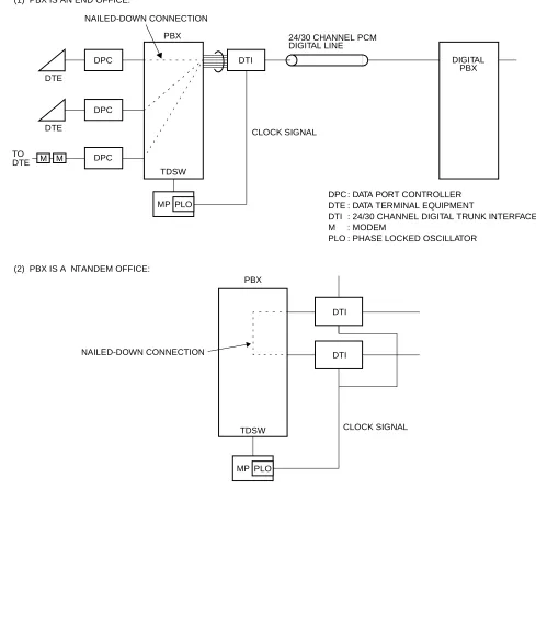
The Data Interface can provide the intra- or inter-office digital data transmission on fixed path (Nailed-Down) connection. The Data Interface equips the V.11 (X.21) and the V.24/V.28 (RS-232C) interface. When you use the V.11 (X.21) interface, a maximum of 64 kbps digital data transmission is available. When you use the V.24/V.28 (RS-232C) interface, a maximum of 19.2 kbps digital data transmission is available.
To add the V.11 (X.21) or V.24/V.28 (RS-232C) Data Interface to the system, it is necessary to install the Data Port Controller (DPC) card. You can provide the V.35 interface DTE by the M03 card installed in addition to the DPC card. The M03 card converts the V.11 (X.21) interface to a V.35 interface. When you provide the inter-office digital data transmission, it is necessary to install the 24/30-channel Digital Trunk Interface (DTI) card in addition to the DPC card.
Figure 1-1 and Figure 1-2 show the outline of the Data Interface intra-office/inter-office connection.
Figure 1-1 System Outline of Intra-Office Data Connection
NOTE: The DPC card can only operate as DCE. If the DPC card is to be connected to a modem
or other DCE, a null modem adapter is required. SYNCHRONOUS
DATA AT SPEEDS OF 56 kbps, 64 kbps
PBX
DTE
DTE
DPC DPC
CHAPTER 1 GENERAL INFORMATION
System Outline
When the PBX is an end office in the Inter-Office Digital Data Transmission through Nailed-Down Connection, the digital signal is transmitted directly. A maximum of 64 kbps digital data transmission is available for the direct digital transmission.
When the PBX is a tandem office in the Inter-Office Digital Data Transmission through Nailed-Down Connection, data transparency is provided, and a maximum of 64 kbps digital data transmission is available.
Table 1-1 shows the connecting pattern of the Inter-Office Data Transmission through Nailed-Down Connection.
: Direct Connection : Tandem Connection — : Not available
Table 1-1 Connecting Patterns
CONNECTING PATTERN
SYSTEM CONFIGURATION TO
FROM LDT/ODT
DTI
(DIGITAL SIGNAL)
DPC — Figure 1-2
LDT/ODT — —
DTI
(Digital Signal)
CHAPTER 1 GENERAL INFORMATION
System Outline
Figure 1-2 System Outline of Inter-Office Data Connection
DTI PBX
(2) PBX IS A NTANDEM OFFICE:
DTI PBX
DTE
DPC DPC
DPC : DATA PORT CONTROLLER DTE : DATA TERMINAL EQUIPMENT
DTI : 24/30 CHANNEL DIGITAL TRUNK INTERFACE M : MODEM
PLO : PHASE LOCKED OSCILLATOR DTE
DPC
M M TO DTE
DTI
MP PLO NAILED-DOWN CONNECTION
24/30 CHANNEL PCM DIGITAL LINE
DIGITAL PBX
CLOCK SIGNAL
TDSW (1) PBX IS AN END OFFICE:
NAILED-DOWN CONNECTION
MP PLO
CHAPTER 1 GENERAL INFORMATION
System Outline
DPC
The Data Port Controller (DPC) can accommodate a maximum of two DTE per cards with V.11 (X.21) or V.24/V.28 (RS-232C) interface, and can provide the intra-office or inter-office digital data transmission on Nailed-Down connection.
DTI
The Digital Trunk Interface (DTI) interfaces the PBX directly to a 24/30-channel PCM transmission line. The DTI has the following functions.
For 24DTI:
• Unipolar/Bipolar Conversion (AMI Format)
• Signaling Insertion/Extraction
• Alarm Detection/Insertion
• Digital PAD on Voice Signal Transmission
• Loopback Test (Local/Remote Loopback)
• Cyclic Redundancy Checking (based on ITU-T Rec. G704)
For 30DTI:
• Unipolar/Bipolar Conversion (HDB3 Format)
• Signaling Insertion/Extraction
• Alarm Detection/Insertion
• Digital PAD on Voice Signal Transmission
• Cyclic Redundancy Checking (based on ITU-T Rec. G704)
• Channel Associated Signaling (based on ITU-T Rec. 0421 Digital R2 Signaling Code)
For connection of a 24DTI and transmission line, twisted-pair cables can be used. For connection of a 30DTI and transmission line, either coaxial cable or twisted pair cable can be used.
M03
The M03 provides V.35 Data Terminal Equipment interface.
CHAPTER 1 GENERAL INFORMATION
System Outline
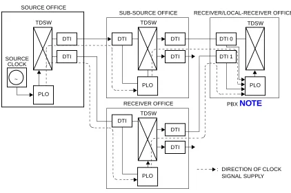
PLO
The Phase Locked Oscillator (PLO) equipped on the MP card synchronizes the system to the digital network clock.
When the PBX is a clock receiver office, the PLO generates the clock signals according to the source clocks received from the source office within the network. The source clock signals are extracted at DTI cards and supplied to the PLO. Two clock routes are available; one is the Route 0 from the source office, and the other is a standby Route 1 from a sub-source office. When no clock signals arrive from the source and sub-source office, due to a transmission line failure, the PLO keeps generating the clock signals at the frequency of the previous source clock. The PLO can receive different frequency of source clocks from the Route 0 and Route 1.
Figure 1-3 shows an example of the clock supply route when the system is a receiver office.
Figure 1-3 Clock Supply Route
PLO TDSW
SOURCE OFFICE
~ SOURCE
CLOCK
RECEIVER/LOCAL-RECEIVER OFFICE
DTI
DTI TDSW RECEIVER OFFICE
DTI
DTI
DTI TDSW SUB-SOURCE OFFICE
PLO DTI
DTI 1 DTI 0 DTI
DTI
PLO
PLO
: DIRECTION OF CLOCK SIGNAL SUPPLY
TDSW
CHAPTER 1 GENERAL INFORMATION
Card Name and Function
CARD NAME AND FUNCTION
Table 1-2 shows the circuit card name and function for Data Interface.
Table 1-2 Card Name and Function
EQUIPMENT NAME
FUNCTIONAL
NAME FUNCTION
PN-CP14 MP Main Processor Card
Provides Memory, TDSW (1024CH × 1024CH), 16-line
CFT, PB sender, Clock, PLO 2 ports (receiver mode/ source mode), two RS-232C ports, 2-line DAT (Recording duration: Max. 128 sec.), DK, 4-line PB receiver, Modem for remote maintenance (19.2 kbps), internal Music-on-Hold tone source and BUS interface. BUS interface functions as a driver/receiver of various signals, adjusts gate delay timing and cable delay timing, monitors I/O Bus and PCM BUS.
One card is required per system.
PN-24DTA-C DTI Digital Trunk Interface (23B + D, 1.5 Mbps) Card
Accommodates 24-channel PCM digital lines.
PN-30DTC-A DTI Digital Trunk Interface (2 Mbps) Card
Accommodates 30-channel PCM digital lines.
PZ-M542
[For Other Countries]
CONN Coaxial Cable Connection Card
Used to connect a coaxial cable for the Digital Trunk Interface.
Two cards maximum can be connected to LTC connector of each PIM.
PZ-M557
[For Australia]
CONN Coaxial Cable Connection Card
Used to connect a coaxial cable for the Digital Trunk Interface.
CHAPTER 1 GENERAL INFORMATION
Card Name and Function
PN-2DPCB DPC 2-line Data Port Controller Card
Used for the intra-office or inter-office digital data transmission on nailed down connection.
Accommodates max. two DTEs with V.11 (X.21) interface or V.24/V.28 (RS-232C) interface.
PN-M03 M03 V.35 Data Terminal Equipment Interface Card
Used together with the PN-2DPCB card to provide the V.35 interface.
Table 1-2 Card Name and Function (Continued)
EQUIPMENT NAME
FUNCTIONAL
CHAPTER 1 GENERAL INFORMATION
System Capacity
SYSTEM CAPACITY
System Capacity for Data Interface
System Capacity for Digital Trunk Interface
Table 1-3 System Capacity for Data Interface
DESCRIPTION CAPACITY REMARKS
DPC Card 50
Circuits per DPC Card 2
Fixed Path Connection 100
Table 1-4 System Capacity for Digital Trunk Interface
DESCRIPTION CAPACITY REMARKS 24DTI 30DTI
DTI Card 8 4
DTI Trunk 192 124
DTI Trunk Route 64 64 1 Route/DTI
CHAPTER 1 GENERAL INFORMATION
System Specifications
SYSTEM SPECIFICATIONS
DPC Specifications
NOTE 1: When the transmission rate is 56 or 64 kbps, only full duplex is available.
NOTE 2: For the transmission rate after Rate Adaptation, see Table 1-6.
Modem Specifications
Table 1-5 DPC Specifications
DESCRIPTION SPECIFICATION
Synchronization Synchronous
Transmission Rate 2.4, 4.8, 9.6, 14.4, 19.2, 48, 56, 64 kbps
Transmission Mode Full/Half Duplex NOTE 1
Rate Adaptation NOTE 2 ITU-T V.110
Table 1-6 Rate Adaptation
TRANSMISSION RATE BEFORE RATE ADAPTATION
TRANSMISSION RATE
AFTER RATE ADAPTATION REMARKS
2.4-4.8 kbps 8 kbps
9.6 kbps 16 kbps
14.4 kbps 32 kbps
19.2 kbps 32 kbps
48-64 kbps 64 kbps
Table 1-7 Modem Specifications
DESCRIPTION SPECIFICATION
CHAPTER 1 GENERAL INFORMATION
System Conditions
SYSTEM CONDITIONS
Time Slot Assignment Condition
As shown in Figure 1-4, the 30DTI card uses the time slot on the basic Highway 4.
Therefore, the total number of time slots for all 30DTI card must be 128 time slots or less including all other application processor cards which use the Highway 4.
The 24DTI card can use the time slot on both the basic and expanded Highway 4 and 6. Therefore, the total number of time slots for all 24DTI card must be 256 time slots or less.
Figure 1-4 Accommodation of DTI into TDSW
PRT
T
D
SW
(1024 T
IME
S
L
O
T
S
)
FP0
FP1
FP2
FP3
DTI
DCH
FOR L/T CARDS: MAX. 512 TIME SLOTS PER SYSTEM
FOR BASIC HIGHWAY4: MAX. 128 TIME SLOTS PER SYSTEM 1 TIME SLOT/CARD
MAX. 128 TIME SLOTS
MAX. 128 TIME SLOTS
MAX. 128 TIME SLOTS
MAX. 128 TIME SLOTS
30DTI: MAX. 31 TIME SLOTS/CARD
BRT
ICH
DTI
MAX. 2 TIME SLOTS/CARD (BRTA) MAX. 4 TIME SLOTS/CARD (2BRTC)
25 TIME SLOT/CARD
24DTI: MAX. 24 TIME SLOTS/CARD 1 TIME SLOT/CARD (SC02) 4 TIME SLOTS/CARD (SC03)
FOR EXPANDED HIGHWAY6: MAX. 128 TIME SLOTS PER SYSTEM HW4
HW6
CHAPTER 1 GENERAL INFORMATION
System Conditions
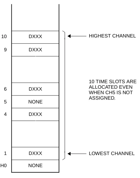
Time Slot Allocation for DTI Card
On each DTI card, the system recognizes the lowest and highest channel numbers to which trunk numbers have been assigned, and allocates time slots to all the channels within them. If trunk numbers are assigned to discontinuous channels in this case, the system also allocates time slots to channels not assigned.
For example, as shown in Figure 1-5, even when Channel 1 through Channel 10 have been
assigned by the system data programming (CM07 YY=01) except Channel 5, the system allocates a total of 10 time slots for all the ten channels. Therefore, to avoid allocation of unnecessary time slots, it is recommended that consecutive channels are assigned on each DTI card.
Figure 1-5 Time Slot Allocation for DTI
10 9
6 5 4
1 CH0
DXXX DXXX
DXXX NONE DXXX
DXXX NONE
LOWEST CHANNEL HIGHEST CHANNEL
CHAPTER 2
INSTALLATION
CHAPTER 2 INSTALLATION
Precautions
PRECAUTIONS
Static Electricity Guard
You must wear a grounded wrist strap to protect circuit cards from static electricity.
Figure 2-1 Static Electricity Guard (1 of 2)
• WHEN PLUGGING/UNPLUGGING A CIRCUIT CARD
• WHEN HOLDING A CIRCUIT CARD
PBX
WRIST STRAP
FRAME GROUND SCREW
CARD FRONT
CHAPTER 2 INSTALLATION
Precautions
Figure 2-1 Static Electricity Guard (2 of 2)
• WHEN MAKING A SWITCH SETTING ON A CIRCUIT CARD
• WHEN CARRYING A CIRCUIT CARD
The mark shown below is attached to the sheet for the work in which circuit cards are handled. When engaging in such work, the installer must be careful not to cause damage by static electricity.
WEAR A WRIST STRAP AND PERFORM THE WORK ON A GROUNDED
CONDUCTIVE WORK SURFACE. CIRCUIT
CARD
WHEN CARRYING A CIRCUIT CARD AROUND, KEEP THE CARD IN A CONDUCTIVE POLYETHYLENE BAG. CIRCUIT
CARD
CONDUCTIVE POLYETHYLENE BAG
ATTENTION
Contents Static Sensitive Handling
CHAPTER 2 INSTALLATION
Precautions
Caution
You must hold the edge of a circuit card when plugging or unplugging the circuit card. If you touch another area, you may be exposed to hazardous voltages.
CARD FRONT
NEVER TOUCH THE COMPONENTS OR SOLDERED SURFACE WITH BARE HANDS.
CHAPTER 2 INSTALLATION
Required Equipment
REQUIRED EQUIPMENT
Table 2-1 shows the equipment required to provide the Data Interface on the system.
Table 2-1 Required Equipment
EQUIPMENT/CABLE DESCRIPTION QTY REMARKS
• PN-2DPCB Data Port Controller Card 1-50
• PN-24DTA-C 24 channel DTI Card 1-8 For Inter-office
• PN-30DTC-A 30 channel DTI Card 1-4 For Inter-office
• PN-M03 V.35 DTE Interface Card 1-50
• PZ-M542/M557 Coaxial Cable Connection
Card
1-4 2 cards/PIM
1 card/DTI
• DPC V11 CABLE Connection Cable between
PN-2DPCB and V.11 (X.21) DTE
N N: Number of V.11
(X.21) DTE 4 m (13.1 ft.)
• 17-TW-0.3 CONN CABLE-A
Connection Cable between PN-2DPCB and PN-M03
N N: Number of V.35 DTE
0.3 m (1 ft.)
• DPC V35 CABLE Connection Cable between
PN-M03 and V.35 DTE
N N: Number of V.35 DTE
4 m (13.1 ft.)
• DPC RS CABLE Connection Cable between
PN-2DPCB and V.24/V.28 DTE
N N: Number of V.24/V.28
DTE
4 m (13.1 ft.)
• MODEM Refer to “Modem
Specifications”. Page 12
2 × N N: Number of DTE
(As required)
(Should be provided by customer.)
• Straight Cable Connection Cable between
DPC V11 CABLE/DPC RS CABLE and DTE
N N: Number of DTE
(When connecting DTE directly)
(Should be provided by customer.)
• Reverse Cable Connection Cable between
DPC V11 CABLE/DPC RS CABLE and Modem
N N: Number of DTE
CHAPTER 2 INSTALLATION
Installation Procedure for Data Interface
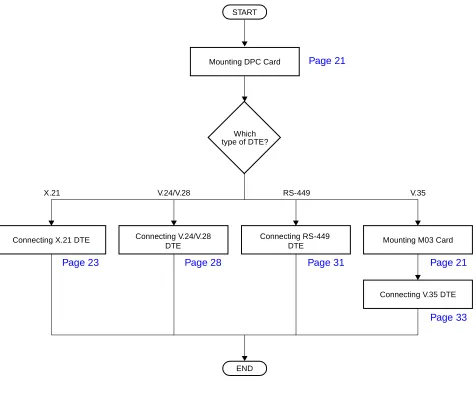
INSTALLATION PROCEDURE FOR DATA INTERFACE
Installation Summary for Data Interface
Install the equipment according to the procedure shown in Figure 2-2.
Figure 2-2 Installation Procedure for Data Interface
START
Mounting DPC Card
END
Page 21
Mounting M03 Card Connecting X.21 DTE Connecting RS-449
Which type of DTE?
DTE Connecting V.24/V.28
DTE
Connecting V.35 DTE
Page 21 Page 31
Page 28 Page 23
Page 33
CHAPTER 2 INSTALLATION
Installation Procedure for Data Interface
Mounting DPC Card
(1) Confirm the correct switch settings of the DPC card. See CHAPTER 5. Page 63.
(2) Mount the DPC cards in LT00 through LT11 slots of PIM0 through PIM7.
Mounting M03 Card
(1) Confirm the correct switch settings of the M03 card. See CHAPTER 5. Page 63.
(2) Mount the M03 cards in LT00 through LT11 slots of PIM0 through PIM7.
ATTENTION
Contents Static Sensitive Handling
CHAPTER 2 INSTALLATION
Installation Procedure for Data Interface
Conditions on Connecting DTE
Forcible ON control of DTR, RTS/C signal:
When connecting the DTE which does not support the DTR signal and RTS/C signal, these signals can be turned to ON forcibly by switch setting on the DPC card.
Condition of CTS signal ON control:
The CTS signal is turned to ON after 60 ms from the time when receiving the RTS/C signal. And the CTS signal is turned to ON under the following conditions.
1. The DTR signal is ON.
2. The received X signal is ON (The synchronization of the opposite office is established). 3. The sending X signal is ON (The synchronization of the PBX is established).
Limitation on using modem:
When using modem, the DTR signal from the DTE can not be transmitted to the PBX (DPC card). Therefore, the DTE starting by the DTR signal can not be used.
Figure 2-3 Limitation on Using Modem
TXD RXD DTR RTS CTS DCD DSR TXC(2) RXC TXD RXD DTR RTS CTS DCD DSR TXC(2) RXC TXC(1) TXD RXD DTR RTS CTS DCD DSR TXC(2) RXC TXC(1) TXD RXD DTR RTS CTS DCD DSR TXC(2) RXC TXD RXD DTR RTS CTS DCD DSR (ON) TXC(2) RXC TXC(1) S-BB TXD RXD DTR RTS CTS DCD DSR TXC(2) RXC TXC(1) ~ X DTR
CHAPTER 2 INSTALLATION
Installation Procedure for Data Interface
Connecting X.21 DTE
Connect the X.21 DTE/modem to the DPC card as shown in Figure 2-4.
Figure 2-4 Cable Connection between DPC Card and X.21 DTE/Modem
(Continued) 2A 2B 3A 3B 4A 4B 5A 5B 6A 4D 3C 6D 6B 2 9 3 10 4 11 5 12 6 8 13 2 9 3 10 4 11 5 12 6 14 7 8 13 T C R I S TXC(1) GND T C R I S GND T C R I S TXC(1) GND XCN0/XCN1 CONNECTOR
STRAIGHT CABLE (LOCALLY PROVIDED)
DPC
X.21 DTE
(J) (J) (P) (P)
4 m (13.1 ft.)
14 7 TXC(1) DPC V11 CABLE
Page 27
(1) Direct Connection
NOTE 1
CHAPTER 2 INSTALLATION
Installation Procedure for Data Interface
NOTE 1: When providing X.21 DTE with TXC(1) signal, this connection is required.
NOTE 2: The distance between the DPC card and X.21 DTE is as follows.
When providing X.21 DTE with TXC(1) signal: L=Max. 1000 m (3281 ft.)
When providing X.21 DTE without TXC(1) signal, the distance depends on the data speed.
(Continued)
Distance (L) Data Speed
Max. 1000 m (3281 ft.) . . . . Max. 800 m (2625 ft.) . . . . Max. 350 m (1148 ft.) . . . . Max. 300 m (984 ft.) . . . . Max. 250 m (820 ft.) . . . .
Less than 9.6 kbps 19.2 kbps
CHAPTER 2 INSTALLATION
Installation Procedure for Data Interface
Figure 2-5 Cable Connection between DPC Card and X.21 DTE/Modem
(Continued) XCN0/XCN1 CONNECTOR
REVERSE CABLE (LOCALLY PROVIDED)
DPC
X.21 MODEM
(J) (J) (P) (P)
4 m (13.1 ft.) 2A 2B 3A 3B 4A 4B 5A 5B 6A 4D 3C 6D 6B 2 9 3 10 4 11 5 12 6 8 13 2 9 3 10 4 11 5 12 6 14 7 8 13 T C R I S TXC(1) GND T C R I S GND T C R I S TXC(1) GND
When using a modem that has not TXC(1) terminal When using a modem that can provide TXC(1) signal
14 7 TXC(1) DPC V11 CABLE
Page 27
(2) Modem Connection
2A 2B 3A 3B 4A 4B 5A 5B 6A 4D 3C 6D 6B 2 9 3 10 4 11 5 12 6 14 7 8 13 T C R I S TXC(1) GND T C R I S GND T C R I S TXC(1) GND TXC(1) 2 9 3 10 4 11 5 12 6 14 7 8 13 TXD RTS RXD DCD TXC(2) NOTE 1
CHAPTER 2 INSTALLATION
Installation Procedure for Data Interface
NOTE 1: When providing X.21 modem with TXC(1) signal, this connection is required.
NOTE 2: The distance between the DPC card and X.21 modem is as follows.
When providing X.21 modem with TXC(1) signal: L=Max. 1000 m (3281 ft.)
When providing X.21 modem without TXC(1) signal, the distance depends on the data speed.
Distance (L) Data Speed
Max. 1000 m (3281 ft.) . . . . Max. 800 m (2625 ft.) . . . . Max. 350 m (1148 ft.) . . . . Max. 300 m (984 ft.) . . . . Max. 250 m (820 ft.) . . . .
Less than 9.6 kbps 19.2 kbps
CHAPTER 2 INSTALLATION
Installation Procedure for Data Interface
Figure 2-6 DPC V11 Cable
.. .. .. .. .. .. . .. ... .. .. .. .
D A (J)
(J) 1 6 1 9 15 8 6D-GND 2A-TA 2B-TB 4A-RA 4B-RB 6A-SA 6B-SB 3C-TXC(1)A 4D-TXC(1)B 3A-CA 3B-CB 5A-IA 5B-IB IA-G 8-GND 2-TA 9-TB 4-RA 11-RB 6-SA 13-SB 7-TXC(1)A 14-TXC(1)B 3-CA 10-CB 5-IA 12-IB 6 5 4 3 2 1 SA IA RA CA TA G A SB IB RB CB TB B X TXC(1) X C GND TXC(1) X D 7 6 5 4 3 2 8 1 TXC(1)A SA IA RA CA TA GND X 14 13 12 11 10 9 15 TXC(1)B SB IB RB CB TB X
CHAPTER 2 INSTALLATION
Installation Procedure for Data Interface
Connecting V.24/V.28 DTE
Connect the V.24/V.28 DTE/modem to the DPC card as shown in Figure 2-7.
Figure 2-7 Cable Connection between DPC Card and V.24/V.28 DTE/Modem
(Continued) 05B 05A 04B 04A 03B 03A 02B 02A 06A 04D 05C 06B GND RXD CTS GND TXC(2) DTR RS0/RS1 CONNECTOR
STRAIGHT CABLE (LOCALLY PROVIDED)
DPC
V.24/V.28 DTE
(J) (J) (P) (P)
4 m (13.1 ft.)
MAX 15 m (49.2 ft.) DPC RS CABLE
CHAPTER 2 INSTALLATION
Installation Procedure for Data Interface
Figure 2-8 Cable Connection between DPC Card and V.24/V.28 DTE/Modem
RS0/RS1 CONNECTOR
REVERSE CABLE (LOCALLY PROVIDED)
DPC
V.24/V.28 MODEM
(J) (J) (P) (P)
4 m (13.1 ft.)
MAX 15 m (49.2 ft.) DPC RS CABLE
CHAPTER 2 INSTALLATION
Installation Procedure for Data Interface
Figure 2-9 DPC RS Cable
.. .. .. .. .. .. . .. ... .. .. .. . D A (J) 1 6 1 14 25 13 05B-GND 02B-GND 05A-TXD 04B-RXD 04A-RTS 03B-CTS 03A-DSR 02A-DCD 05C-DTR 04D-TXC(1) 06A-TXC(2) 06B-RXC 01C-RI 01A-GND 1-GND 7-GND 2-TXD 3-RXD 4-RTS 5-CTS 6-DSR 8-DCD 20-DTR 24-TXC(1) 15-TXC(2) 17-RXC 22-RI 06 05 04 03 02 01 TXC(2) TXD RTS DSR DCD G A RXC GND RXD CTS GND B DTR X RI C X TXC(1) X D 12 11 10 9 8 7 13 6 X X X X DCD GND X DSR 24 23 22 21 20 19 25 TXC(1) X RI X DTR X X
CHAPTER 2 INSTALLATION
Installation Procedure for Data Interface
Connecting RS-449 DTE
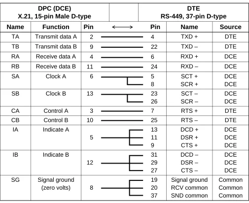
RS-449 DTE requires a locally provided conversion cable, as shown in Figure 2-10. This cable must be equipped with a 15-pin male D-type connector and a 37-pin D-type connector (male or female as required by DTE.) A modification is required to be installed in the 37-pin connector, as shown in the Table 2-2, Figure 2-11 and Figure 2-12.
Figure 2-10 Cable Connection between DPC Card and RS-449 DTE
Table 2-2 X.21 to RS-449 Adapter Cable Connections
DPC (DCE)
X.21, 15-pin Male D-type
DTE
RS-449, 37-pin D-type Name Function Pin Pin Name Source
TA Transmit data A 2 4 TXD + DTE
TB Transmit data B 9 22 TXD – DTE
RA Receive data A 4 6 RXD + DCE
RB Receive data B 11 24 RXD – DCE
SA Clock A 6 5
8
SCT + SCR +
DCE DCE
SB Clock B 13 23
26
SCT – SCR –
DCE DCE
CA Control A 3 7 RTS + DTE
CB Control B 10 25 RTS – DTE
IA Indicate A 13
5 11 9 DCD + DSR + CTS + DCE DCE DCE
IB Indicate B 31
12 29 27 DCD – DSR – CTS – DCE DCE DCE
SG Signal ground
(zero volts) 19 8 20 37 Signal ground RCV common SND common Common Common Common XCN0/XCN1 CONNECTOR X.21 to RS-449 ADAPTER CABLE
DPC
RS-449 DTE
(J) (J) (P) (J/P)
DPC V11 CABLE
Page 27
CHAPTER 2 INSTALLATION
Installation Procedure for Data Interface
Figure 2-11 RS-449 Connector Pin Assignments
Figure 2-12 X.21 Connector Pin Assignments
Source Signal Common DCE Return DTE DCE DTE Return Return Return DTE Return Return Return Return Return Return Ð Send Common Standby Indicator Terminal Timing (B) New Signal Signal Quality Select Standby Receiver Ready (B) Terminal Ready (B) Data Mode (B) Terminal in Service Clear To Send (B) Receive Timing (B) Request To Send (B) Receive Data (B) Send Timing (B) Send Data (B) Unassigned Common Receive Common
Source Signal Common DCE DTE DTE DCE DTE DCE DTE DCE DTE DCE DCE DTE DCE DCE DTE Ð DCE Common Signal Ground
Test Mode (A) Terminal Timing (A) Select Frequency Incoming Call Remote Loopback Receiver Ready (A) Terminal Ready (A) Data Mode (A) Local Loopback Clear To Send (A) Receive Timing (A) Request To Send (A) Receive Data (A) Send Timing (A) Send Data (A) Unassigned
Signal Rate Indicator Shield 20 1 21 2 22 3 23 4 24 5 25 6 26 7 27 8 28 9 29 10 30 11 31 12 32 13 33 14 34 15 35 16 36 17 37 18 19 Source Signal Ð DCE DCE DCE Unassigned Byte Timing (B) Signal Element Timing (B)
Indication (B) Source Signal Common DCE DCE DCE Signal Ground
Byte Timing (A)
CHAPTER 2 INSTALLATION
Installation Procedure for Data Interface
Connecting V.35 DTE
(1) Connect the M03 card and the DPC card as shown in Figure 2-13.
(2) Connect the V.35 DTE/modem to the M03 card in the following pages.
Figure 2-13 Outline of V.35 Cable Connection
DPC
V.35 DTE/ 17-TW-0.3 CONN CABLE
DPC V35 CABLE M03
PBX
V.35 INTERFACE CABLE
MODEM XCN0/XCN1 CONNECTOR
X21 CONNECTOR
V35 CONNECTOR
CHAPTER 2 INSTALLATION
Installation Procedure for Data Interface
Figure 2-14 Cable Connection between M03 Card and V.35 DTE/Modem
NOTE: When you provide V.35 DTE using TXC(1) signal, this connection is required.
(Continued) V35 CONNECTOR
STRAIGHT CABLE (LOCALLY PROVIDED)
M03
V.35 DTE
(J) (J) (P) (P)
4 m (13.1 ft.)
MAX 15 m (49.2 ft.) TXD 4A 4B RXD 2A 2B RTS 6A CTS 6B DSR 5A GND 6D DCD 5B TXC(2) 3A 3B RXC 1C 2D DTR 5C TXC(1) 3C 4D TXD P S RXD R T RTS C CTS D DSR E GND B GND A DCD F TXC(2) Y AA RXC V X DTR H TXC(1) U W TXD P S RXD R T RTS C CTS D DSR E GND B GND A DCD F TXC(2) Y AA RXC V X DTR H TXC(1) U W NOTE
DPC V35 CABLE
Page 36
CHAPTER 2 INSTALLATION
Installation Procedure for Data Interface
Figure 2-15 Cable Connection between M03 Card and V.35 DTE/Modem
V35 CONNECTOR
REVERSE CABLE (LOCALLY PROVIDED)
M03
V.35 MODEM
(J) (J) (P) (P)
4 m (13.1 ft.)
MAX 15 m (49.2 ft.) TXD 4A
4B RXD 2A 2B RTS 6A CTS 6B DSR 5A GND 6D DCD 5B TXC(2) 3A 3B RXC 1C 2D DTR 5C TXC(1) 3C 4D
TXD P
S
RXD R
T
RTS C
CTS D
DSR E
GND B
GND A
DCD F
TXC(2) Y AA
RXC V
X
DTR H
TXC(1) U W
TXD P
S
RXD R
T
RTS C
CTS D
DSR E
GND B
GND A
DCD F
TXC(2) Y AA
RXC V
X
DTR H
TXC(1) U W (2) Modem Connection
DPC V35 CABLE
CHAPTER 2 INSTALLATION
Installation Procedure for Data Interface
Figure 2-16 DPC V35 Cable
D A (J)
CHAPTER 2 INSTALLATION
Installation Procedure for Data Interface
Figure 2-17 V.35 Connector Pin Assignment
Table 2-3 V.35 Interface Cable Connector Pin Assignments
Pin Name Function Specification Source
A B C D E F H GND GND RTS CTS DSR RLSD DTR Frame Ground Signal Ground Request To Send Clear To Send Data Set Ready
Received Line Signal Detector Data Terminal Ready
— — RS-232 RS-232 RS-232 RS-232 RS-232 — — DTE DCE DCE DCE DTE P S
TXD Send Data V.35 DTE
R T
RXD Receive Data V.35 DCE
U W
SCTE Serial Clock Transmit External (A)
Serial Clock Transmit External (B)
V.35 DTE
V X
SCR Serial Clock Receive (A)
Serial Clock Receive (B)
V.35 DCE
Y
AA (or aa)
SCT Serial Clock Transmit (A)
Serial Clock Transmit (B)
V.35 DCE
L, M, N, Z, BB, CC, DD, EE, HH, JJ, KK, LL, MM, NN
Reserved for future V.35 use
B F R V D T X Signal Pin
Chassis Ground A Request To Send C Data Set Ready E Data Terminal Ready H Transmitted Data P Transmitted Data S Transmit Timing U Transmit Timing W Transmit Timing Y Transmit Timing AA
Pin Signal
B Signal Ground D Clear To Send F Receive Line Signal
Detect
R Received Data T Received Data V Receive Timing X Receive Timing
CHAPTER 2 INSTALLATION
Installation Procedure for Data Interface
INSTALLATION PROCEDURE FOR DIGITAL TRUNK
INTERFACE
Installation Summary for Digital Trunk Interface
Install the equipment according to the procedure shown in Figure 2-18.
Figure 2-18 Installation Procedure for DTI
NOTE: This procedure is required when you provide CONN card to connect a coaxial cable for
30DTI.
START
Selection of PLO in MP Card Mounting DTI Card
DTI Cable Connection
Page 39
CHAPTER 5 Page 63
Page 40
via MDF
Mounting CONN Card Page 39 NOTE
END DTI Cable Connection
Page 43 NOTE
CHAPTER 2 INSTALLATION
Installation Procedure for Data Interface
Mounting DTI Card
(1) Before mounting the DTI (PN-24DTA-C/PN-30DTC-A) card, set the MB
switch to UP position, and set the other switches to appropriate position. See CHAPTER 5.Page 63
(2) Mount the DTI card in the following AP slots on PIM0-PIM7.
PIM0: AP00-AP10 slots
PIM1-7: AP00-AP11 slots
After mounting the card, set the MB to DOWN position to put the card in service.
NOTE: The DTI card (DTI 0, DTI 1) which sends a clock signal to PLO of the MP card must be
mounted in the AP slots on PIM0.
Mounting CONN Card
When you provide CONN (PZ-M542/M557) card to connect a coaxial cable for 30DTI, do the following installation.
(1) Confirm the correct switch settings of the CONN card. See CHAPTER 5.Page 63
(2) Mount the CONN card on LTC connector on BWB in the PIM which accomodates the DTI
cards.
For details, refer to the Installation Procedure Manual.
ATTENTION
Contents Static Sensitive Handling
CHAPTER 2 INSTALLATION
Installation Procedure for Data Interface
DTI Cable Connection via MDF
When you use a twisted-pair cable, connect the cable to a CSU via the MDF as shown below.
• Location of AP Slots and LTC Connectors for DTI - Page 41
• Example of MDF Cross Connection for DTI - Page 42
Figure 2-19 DTI Cable Connection via MDF
CSU MDF
LTC0/LTC1/LTC2/LTC3 CONNECTOR TWISTED-PAIR CABLE BWB
PBX (PIM0-PIM7)
MAX. 200 m (655 ft.)
Figure 2-20, Figure 2-21,
Figure 2-22, Figure 2-23
CHAPTER 2 INSTALLATION
Installation Procedure for Data Interface
Figure 2-20 Location of the AP Slots and the LTC Connectors for DTI
CHAPTER 2 INSTALLATION
Installation Procedure for Data Interface
Figure 2-21 Example of MDF Cross Connection for DTI
17 18 19 20
RA TA
42 43 44 45
RB TB LTC1 (J)
42 43 44 45
RB TB
17 18 19 20
RA TA LTC1 (P) PIM 0
J P MDF
DTI
AP05
RA RB TA TB
17 42 18 43
17 42 18 43
RA RB TA TB
TO CSU LTC1
RECEIVE
CHAPTER 2 INSTALLATION
Installation Procedure for Data Interface
DTI Cable Connection via CONN Card
When you use an coaxial cable, connect the cable to a CSU via the CONN (PZ-M542/M557) card as shown in Figure 2-22.
Figure 2-23 shows an example of the cable connection when the 30DTI card is mounted in the AP05 slot of PIM0.
Figure 2-22 DTI Cable Connection via CONN Card
CSU
LTC0/LTC1/LTC2/LTC3
COAXIAL CABLE 30DTI
BWB PBX
MAX. 6 dB loss at 1024 kHz CONN
CHAPTER 2 INSTALLATION
Installation Procedure for Data Interface
Figure 2-23 Example of Coaxial Cable Connection
2 COAXIAL CONNECTOR 1 LTC1 CONNECTOR
LTC1 (J) LTC1 (P) PIM0
J P CONN
30DTI
AP05
RA RB TA TB
17 42 18 43
17 42 18 43
TO CSU LTC1
RECIEVE RCV
TRANSMIT TRS
17 18 19 20
RA TA
42 43 44 45
RB TB
17 18 19 20 RB TB 42 43 44 45
RA TA
CHAPTER 3
SYSTEM DATA
PROGRAMMING
CHAPTER 3 SYSTEM DATA PROGRAMMING
How to Read This Chapter
HOW TO READ THIS CHAPTER
In the programming procedure, the meaning of (1), (2) and markings are as follows.
(1) : 1st Data
(2) : 2nd Data
: Initial Data; With the system data clear command (CM00, CM01), the data with this marking is automatically set for each command.
: A reset of the MP card is required after data setting. Press SW1 switch on the MP card.
:A reset of the DTI card is required after data setting. Set the Make Busy switch to UP and then DOWN. INITIAL
CHAPTER 3 SYSTEM DATA PROGRAMMING
Data Interface Assignment
DATA INTERFACE ASSIGNMENT
DESCRIPTION DATA
To assign data station number by CM1A, assign a station number (dummy number) to each port (LEN) on the DPC card.
NOTE 1: The station number must be
assigned to the first LEN (level 0) and the third LEN (level 2) of each LT slot (The station number must be also assigned to the unused port on the DPC card).
NOTE 2: The “*” and “#” can not be used as a station number.
(1) (2)
000-763: LEN
FX-FXXXXXXXX: Station No. X: 0-9
Assign a data station number to the station number assigned by CM10.
NOTE: The data station number must be also assigned to the unused port on the DPC card.
(1)
(2)
X-XXXXXXXX: Station No. assigned by CM10
X-XXXXXXXX: Data Station No.
Assign an access code for data station. • (1) (2)
Y=0-3 Numbering Plan Group 0-3 X-XXXX: Access Code
801: 1 digit station 802: 2 digits station 803: 3 digits station 804: 4 digits station 805: 5 digits station 806: 6 digits station 807: 7 digits station 808: 8 digits station Assign the type of data terminal interface
to the data station number.
NOTE: This data must be also assigned to the unused port on the DPC card.
(1) (2)
X-XXXXXXXX: Data Station No. 04: DPC
CM1A
CM20 START
CM10
CMA0
A
INITIAL
CHAPTER 3 SYSTEM DATA PROGRAMMING
Data Interface Assignment
DESCRIPTION DATA
Assign the attribute data for data station (assigned by CM1A) in accordance with the specification of the DTE connected.
• (1) (2)
YY=04 Data speed
X-XXXXXXXX: Data Station No. 00-05 : 1200 bps
06 : 600 bps 07 : 1200 bps 08 : 2400 bps 09 : 4800 bps 10 : 9600 bps 11 : 19.2 kbps 12 : 48 kbps 13 : 56 kbps 14 : 64 kbps 15 : 7200 bps 16 : 14.4 kbps 17-31 : 1200 bps
• (1) (2)
YY=05 Parity Check
X-XXXXXXXX: Data Station No. 0 : Effective
1 : Ineffective
• (1) (2)
YY=06 Synchronous/Asynchronous X-XXXXXXXX: Data Station No. 0 : Synchronous
7 : Asynchronous
• (1) (2)
YY=07 Transmission Mode X-XXXXXXXX: Data Station No. 0 : Half Duplex
1 : Full Duplex A
CHAPTER 3 SYSTEM DATA PROGRAMMING
Data Interface Assignment
DESCRIPTION DATA
• (1) (2)
YY=08 Stop Bit
X-XXXXXXXX: Data Station No. 0 : 2-Stop Bit
1 : 1-Stop Bit
(1) (2)
YY=09 Type of Code
X-XXXXXXXX: Data Station No. 00 : ASCII (7-bit) + even parity 01 : ASCII (7-bit) + odd parity 02 : ASCII (7-bit) + parity (0) 03 : ASCII (7-bit) + parity (1) 04 : JIS (7-bit) + even parity 05 : JIS (7-bit) + odd parity 06 : JIS (8-bit)
07 : EBCDIC (8-bit)
15 : Non character (Binary Data)
• (1) (2)
YY=19 S Buffer
X-XXXXXXXX: Data Station No. 0 : Effective
1 : Ineffective
Provide the Nailed-Down Connection with the connecting patterns.
•
(1)
(2)
YYY=00-99, 000-199
Memory Block 00-99, 000-199 X-XXXXXXXX: Data station No.
assigned by CM1A DXXX : Trunk No.
assigned by CM07
X-XXXXXXXX: Data station No. assigned by CM1A DXXX : Trunk No.
assigned by CM07 CMA1 B END CMA5 1ST DATA (1) 2ND DATA (2)
Data station to Data station
X-XXXX XXXX
X-XXXX XXXX Data station to trunk X-XXXX
XXXX DXXX Trunk to trunk
(Tandem Connection) DXXX DXXX
CHAPTER 3 SYSTEM DATA PROGRAMMING
Digital Trunk Interface Assignment
DIGITAL TRUNK INTERFACE ASSIGNMENT
DESCRIPTION DATA
Assign an AP number to the DTI card. The AP number must match the SENSE switch setting on the DTI card.
• (1) (2)
Y=0
04-15, 20-31: AP No. 09: DTI
Specify the AP highway channel for 24DTI card.
• (1) (2)
Y=1
04-15, 20-31: AP No.
0 : Expanded Highway channel (128 time slots)
1 : Basic Highway channel (128 time slots)
Assign trunk numbers to each channel number on the DTI card.
The system allocates time slots to consecutive channels from the lowest to the highest channel number assigned. To minimize the number of time slots
allocated, assign trunk numbers to consecutive channels on each card. Never skip channels in CM07.
• (1)
(2)
YY=01 XX ZZ
XX: 04-15, 20-31: AP No. assigned by CM05 Y=0
ZZ: 00-23: Channel No. of 24DTI 01-15, 17-31: Channel No. of
30DTI D000-D255: Trunk No.
Any trunk number already assigned by CM10 cannot be used.
CM07 START
CM05
A
INITIAL
INITIAL
CHAPTER 3 SYSTEM DATA PROGRAMMING
Digital Trunk Interface Assignment
DESCRIPTION DATA
Assign the necessary functions to the 24DTI card.
After entering the data, set the MB switch on the DTI card to UP, and then to DOWN, for DTI initialization.
• (1)
(2)
(1)
(2)
(1)
(2)
(1)
(2)
YY=00 Data Mode
04-15, 20-31: AP No. assigned by CM05 Y=0
0: Based on AT&T Spec.
YY=01 Frame Configuration 04-15, 20-31: AP No. assigned by CM05 Y=0
0 : 12-Multi Frame 1 : 24-Multi Frame
YY=02 Zero Code Suppression 04-15, 20-31: AP No. assigned by
CM05 Y=0
1 : Not available (Transparent)
YY=03
04-15, 20-31: AP No. assigned by CM05 Y=0
7 : Associated Channel Interoffice Signaling
Assign a trunk route number for tie line interface to each DTI.
NOTE: The DTI route must be separated from any analog trunk route.
• (1)
(2)
YY=00
000-255: Trunk No. assigned by CM07 Y=01
00-63: Trunk Route No.
Assign trunk route data to each DTI route. • (1) (2)
YY=00 Kind of Trunk Route 00-63: Trunk Route No. 04: Tie Line trunk
• (1) (2)
YY=01 Dialing Signal Type 00-63: Trunk Route No. 7 : DP/DTMF (Incoming)
DTMF (Outgoing) CMAA
A
CM30
CM35
B
CHAPTER 3 SYSTEM DATA PROGRAMMING
Digital Trunk Interface Assignment
DESCRIPTION DATA
CM35 Y=19 DTI PAD [For Australia]
[For North America/Other Countries]
•
(1) (2)
YY=04
Answer Signal from distant office 00-63: Trunk Route No.
2: Answer signal arrives
•
(1) (2)
YY=05
Release Signal from distant office 00-63: Trunk Route No.
1 : Release signal arrives
• (1) (2)
YY=09 Incoming Connection Signaling 00-63: Trunk Route No.
03: Wink Start 04: Delay Dial 05: Immediate Start
06: 2nd DT/Timing Start-Tie Line
• (1) (2)
YY=19 DTI Pad
00-63: Trunk Route No.
0-3: Programmable PAD by CM42 4-7 : Fixed PAD (See left table)
• (1) (2)
YY=20 Sender start condition 00-63: Trunk Route No. 00 : Wink Start 01 : Delay Dial 02 : Ground Start 15 : Timing Start
•
(1) (2)
YY=89 Cyclic Redundancy Checking for Bit Error Detection
00-63: Trunk Route No. 0: To provide
CM35 B
C
T/R: Transmitter PAD/Receiver PAD
CONNECTION PATTERNS
PAD DATA OF DTI [dB] DATA =4 (T/R) DATA =5 (T/R) DATA =6 (T/R) DATA =7 (T/R) Station-DTI 0/0 Tone-DTI 0/0 COT/DID/LDT-DTI 0/0 ODT-DTI 0/0 DTI-DTI 0/0
T/R : Transmitter PAD/Receiver PAD + : Gain
– : Loss
CONNECTION PATTERNS
PAD DATA OF DTI [dB]
DATA =4 (T/R) DATA =5 (T/R) DATA =6 (T/R) DATA =7 (T/R)
Station-DTI –3/–8 –3/–3 –3/–3 –3/–8 Tone-DTI 0/0 0/0 0/0 0/0
COT/DID/LDT/ODT (2W E&M)-DTI
0/0 0/0 0/0 0/0
ODT (4W E&M)-DTI
+3/–3 0/0 0/0 +3/–3
CHAPTER 3 SYSTEM DATA PROGRAMMING
Digital Trunk Interface Assignment
DESCRIPTION DATA
Specify the kind of digital data transmission.
• (1) (2)
YY=92
00-63: Trunk Route No.
0 : Digital Data Transmission (48 kbps)
1 : Digital Data Transmission (56 kbps)
2 : Digital Data Transmission (Transparent)
3 : Reversal of F&S Bits
7 : Data Transmission via Modem CM35
C
CHAPTER 4
OPERATION TEST
CHAPTER 4 OPERATION TEST
DPC Loopback Test
DPC LOOPBACK TEST
This test is the intra-office loopback test on the DPC card using a modem tester. There are two kinds of loopback (Loopback 1, Loopback 2) as shown in Figure 4-1. Either the Loopback 1 or the Loopback 2 can be selected by switch settings on the DPC card.
Figure 4-1 DPC Loopback Tests
V.110 DPC V.110 DPC
Loopback 1 PBX
MODEM TESTER
DTI
Loopback 2
MODEM TESTER
DTI
CHAPTER 4 OPERATION TEST
DPC Loopback Test
DPC Loopback 1 Test
(1) Set the SW1 on the DPC card as shown below.
(2) Confirm whether the LB01 lamp (for No. 0 circuit) or the LB11 lamp (for No. 1 circuit) on the DPC card lights.
• If the LB01 lamp or the LB11 lamp does not light, check the switch settings on the DPC card and the system data assignment.
(3) Connect a modem tester to the DPC card as shown in Figure 4-2.
Figure 4-2 Connection of Modem Tester
For No. 0 Circuit For No. 1 Circuit
4 3 2 1 OFF
ON SW1
4 3 2 1 OFF
ON SW1
: POSITION TO BE SET
MODEM TESTER
DPC
PBX
(J) (P)
STRAIGHT CABLE DPC V11 CABLE
(P) (J)
XCN0 (FOR No. 0 CIRCUIT)/ XCN1 (FOR No. 1 CIRCUIT)
CHAPTER 4 OPERATION TEST
DPC Loopback Test
(4) Set the attributes of modem tester (transmission rate, etc.).
(5) To confirm whether the data is transmitted correctly, send the PN Pattern 9 (511 Pattern) from the modem tester.
(6) Count bit errors on the modem tester for 1 minute.
• If bit errors do not occur, the cable connection between DPC card and modem tester is normal.
(7) If bit errors occur, check the cable connection, and replace the DPC card.
CHAPTER 4 OPERATION TEST
DPC Loopback Test
DPC Loopback 2 Test
After you complete the DPC Loopback 1 Test, do the following steps.
(1) Set the SW1 on the DPC card as shown below.
(2) Confirm whether the LB02 lamp (for No. 0 circuit) or the LB12 lamp (for No. 1 circuit) on the DPC card lights.
• If the LB02 lamp or the LB12 lamp does not light, check the switch settings on the DPC card and the system data assignment.
(3) Connect a modem tester to the DPC card as shown in Figure 4-2 “Connection of Modem Tester.”
(4) Set the attributes of modem tester (transmission rate, etc.).
(5) To confirm whether the data is transmitted correctly, send the PN Pattern 9 (511 Pattern) from the modem tester.
(6) Count bit errors on the modem tester for 1 minute.
For No. 0 Circuit For No. 1 Circuit
4 3 2 1 OFF
ON SW1
4 3 2 1 OFF
ON SW1
CHAPTER 4 OPERATION TEST
Other Loopback Tests
OTHER LOOPBACK TESTS
Two additional forms of loopback test are shown in Figure 4-3.
Figure 4-3 Other Loopback Tests
V.110 DPC
DTI local loopback PBX
DTI
DTI hard-wired loopback
Set DTI in local loopback.
DTI
TA TB RA RB
On the MDF, connect transmit leads to the Receive leads to test all portions of the DTI. V.110
DPC
CHAPTER 4 OPERATION TEST
Inter-Office Digital Data Transmission Test
INTER-OFFICE DIGITAL DATA TRANSMISSION TEST
This test is the inter-office digital data transmission test using modem testers. After you complete the loopback tests, do the following steps.
(1) Connect modem testers to the both PBXs as shown in Figure 4-4.
Figure 4-4 Inter-Office Digital Data Transmission Test
(2) Set the attributes of both modem testers (transmission rate, etc.).
NOTE: If both the attributes do not match, this test is not available.
(3) To confirm whether the data is transmitted correctly, send the PN Pattern 9 (511 Pattern) from the modem testers.
(4) Count bit errors on the modem testers for 1 minute.
• If bit errors do not occur, the inter-office digital data transmission is normal. PBX
PBX
MODEM TESTER
DTI
DPC DTI DPC
MODEM TESTER 24/30 CHANNEL
PCM DIGITAL LINE
NOTE 1: For details of cable connection between the DPC card and the modem tester, see
Figure 4-2 “Connection of Modem Tester.”
NOTE 2: The modem tester is locally provided.
CHAPTER 5
CIRCUIT CARD
INFORMATION
CHAPTER 5 CIRCUIT CARD INFORMATION
How to Read This Chapter
HOW TO READ THIS CHAPTER
This chapter explains each circuit card used in this system for the following items. Explanations are given in the alphabetical order of the circuit card names within each circuit card category (Control, Application Processor, and Line/Trunk).
(1) Locations of Lamps, Switches, and Connectors
The locations of lamps, switches, and connectors of each circuit card are shown by a face layout.
(2) Lamp Indications
The name, color, and functions of each indicator lamp equipped on each circuit card are described in a table.
(3) Switch Settings
The name, settings, and functions of each switch equipped on each circuit card are described in a table.
CHAPTER 5 CIRCUIT CARD INFORMATION
Mounting Location of Circuit Card
MOUNTING LOCATION OF CIRCUIT CARD
This section explains the conditions for mounting circuit cards for the Data Interface. Figure 5-1 shows circuit card mounting slots allocated in the PIM.
Figure 5-1 Mounting Location of Circuit Card
*1 PN-CP14 (MP) card on the MP12 slot on PIM0.
*2 PN-24DTA-C/PN-30DTC-A (DTI) card on the AP00-AP11 slots on PIM0-PIM7. *3 PN-2DPCB (DPC) and PN-M03 (M03) card on the LT00-LT11 slots on PIM0-PIM7.
*4 PZ-M542/PZ-M557 (CONN) card on the LTC0-LTC3 connectors on the PIM which
accommodates 30DTI card.
LT 09/ AP09 LT 08/ AP08 LT 07/ AP07 LTC1 LTC0 LTC2 BWB PIM 0~7 FRONT AC/DC PWR LT 10/ AP10 LT 00/ AP 00 LT 01/ AP01 LT 02/ AP02 LT 03/ AP03 LT 04/ AP04 LT 05/ AP05 LT 06/ AP06 LT 11/ AP11 /F P 11 MP 12/ F P 12 LTC3 DC/DC PWR PF T VM
*2, *3 *1
CHAPTER 5 CIRCUIT CARD INFORMATION
List of Required Circuit Cards
LIST OF REQUIRED CIRCUIT CARDS
Table 5-1 shows the required circuit cards to be explained in this section.
*MB = Make Busy
Table 5-1 List of Required Circuit Cards
NAME (FUNCTIONAL
NAME)
LAMP
X: PROVIDED –: NOT
PROVIDED
SWITCH X: PROVIDED –: NOT
PROVIDED
EXTRACTION/ INSERTION WITH POWER ON
X: ALLOWED : ALLOWED
AFTER MB* –: NOT ALLOWED
REFERENCE PAGE
PN-CP14 (MP) X X – Page 67
PN-24DTA-C (DTI) X X Page 72
PN-30DTC-A (DTI) X X Page 78
PZ-M542 (CONN) – X X Page 84
PZ-M557 (CONN) – X X Page 86
PN-2DPCB (DPC) X X X Page 88
CHAPTER 5 CIRCUIT CARD INFORMATION
List of Required Circuit Cards
PN-CP14 (MP)
Locations of Lamps, Switches, and Connectors
CONN: To CONNR connector on PZ-M537 (EXPMEM)
Lamp Indications
LAMP
NAME COLOR FUNCTION
RUN Green Flashes at 120 IPM while this card is operating normally.
CLK Green Remains lit while receiving clock signals to the PLO.
SW3 RUN SW1
SW2
CLK VR
DK JACK CONN
SW4
JP0 JP1
CHAPTER 5 CIRCUIT CARD INFORMATION
List of Required Circuit Cards
Switch Settings
CAUTION
When the operating power is being supplied to this circuit card, do not plug/unplug this circuit card into/from its mounting slot.
SWITCH NAME SWITCH NUMBER
SETTING
POSITION FUNCTION CHECK
SW3 (Rotary SW)
NOTE 1
0-F
On Line
(Call processing is in progress)
2 Off Line (Call processing is stopped)
• I/O port: As per CM40 YY=08
3 Off Line (Call processing is stopped)
• I/O port: 9600bps (Fixed)
5
NOTE 2
Off Line (Call processing is stopped) • I/O port: 9600bps
6
NOTE 2
Off Line (Call processing is stopped) • I/O port: 19200bps
7
NOTE 2
Off Line (Call processing is stopped) • I/O port: 38400bps
8
NOTE 2
Off Line (Call processing is stopped) • I/O port: 57600bps
B For clearing the office data
C For setting the resident system
program
1, 4, 9 A, D-F
Not used 0
CHAPTER 5 CIRCUIT CARD INFORMATION
List of Required Circuit Cards
SWITCH NAME SWITCH NUMBER
SETTING
POSITION FUNCTION CHECK
SW1 (Push SW) For initializing CPU
SW2
(Piano Key SW) 1
ON A-law (Australia)
OFF µ-law (North America)
2, 3
Selection of PLO0 input (Phase Locked Oscillator) • For clock receiver office:
• For clock source office:
SW2-2 SW2-3
OFF OFF
4 ON
When using RS1 port for built-in MODEM
OFF When using RS1 port for RS-232C
(Continued) 4
3 2 1 OFF
ON SW2-2 SW2-3 FUNCTION
OFF OFF 1.5 MHz clock
[For PN-24DTA-C/PN-24PRTA]
ON OFF 192 kHz clock [For PN-BRTA]
OFF ON 2 MHz clock
[For PN-30DTC-A/PN-2BRTC]
CHAPTER 5 CIRCUIT CARD INFORMATION
List of Required Circuit Cards
SWITCH NAME SWITCH NUMBER
SETTING POSITIO
N
FUNCTION CHECK
SW4 (Dip SW) 1 Not used
2 Not used
3, 4
Selection of PLO1 input (Phase Locked Oscillator) • For clock receiver office:
• For clock source office:
SW4-3 SW4-4
OFF OFF
VR (Rotary SW) Variable Resister for External Hold
Tone Source
(0 - 20 Kohms : Clockwise)
DK (Connector) 02 Ground detection
01 Ground sending
1 2 3 4 ON
OFF
OFF
SW4-3 SW4-4 FUNCTION
OFF OFF 1.5 MHz clock
[For PN-24DTA-C/PN-24PRTA]
ON OFF 192 kHz clock [For PN-BRTA]
OFF ON 2 MHz clock
[For PN-30DTC-A/PN-2BRTC]
ON ON Not used
20 0
CHAPTER 5 CIRCUIT CARD INFORMATION
List of Required Circuit Cards
The figure in the SWITCH NAME column and the position in in the SETTING POSITION
column indicate the standard setting of the switch. When the switch is not set as shown by the figure and , the setting of the switch varies with the system concerned.
SWITCH NAME SWITCH NUMBER
SETTING
POSITION FUNCTION CHECK
JP0 (Jumper pin)
UP Not used
(Memory backup OFF)
For normal operation (Memory backup ON)
JP1 (Jumper pin)
For using internal tone source
DOWN For using external tone source
Front DOWN
Front
CHAPTER 5 CIRCUIT CARD INFORMATION
List of Required Circuit Cards
PN-24DTA-C (DTI)
Locations of Lamps, Switches and Connectors
SENSE RUN MB
CRC PCM FRM RMT AIS BL SW1
SW0
JRR1
AISS MAS
JPR0
CHAPTER 5 CIRCUIT CARD INFORMATION
List of Required Circuit Cards
Lamp Indications
LAMP
NAME COLOR FUNCTION
RUN Green Flashes at 120 IPM while this card is operating normally.
CRC Red Remains lit when detecting Cyclic Redundancy Checking (CRC)
errors.
PCM Red Remains lit when detecting PCM signal loss.
FRM Red Remains lit when detecting Frame Alignment signal loss.
RMT Red Remains lit when receiving Frame Alignment signal loss alarm
from a distant office.
AIS Red Remains lit when a pattern of consecutive “1” is received. The
distant office transmits this signal for a loop-back test.
BL Red B channel status
ON : More than 10 channels are busy
OFF : All channels are idle
Flash (60 IPM) : Only one channel is busy
CHAPTER 5 CIRCUIT CARD INFORMATION
List of Required Circuit Cards
Switch Settings
SWITCH NAME SWITCH NUMBER
SETTING
POSITION FUNCTION CHECK
SENSE (Rotary SW)
NOTE 1
0-3 Not used
4-F Set the switch to match the AP Number (04-31) to
be set by CM05.
MB (Toggle SW)
NOTE 2
UP For make-busy
For normal operation
(Continued) F
4
AP No. SW1-4: ON
04 05 06 07 08 09 10 11 12 13 14 15
SW1-4: OFF 20 21 22 23 24 25 26 27 28 29 30 31
SW No. 4 5 6 7 8 9 A B C D E F
ON
CHAPTER 5 CIRCUIT CARD INFORMATION
List of Required Circuit Cards
SW0
(Piano Key SW) 1
NOTE 3 NOTE 4
ON Source clock signal from network is
sent to the PLO 0 input on MP card.
OFF
Source clock signal from network is not sent to the PLO 0 input on MP card.
2
NOTE 3 NOTE 4
ON Source clock signal from network is
sent to the PLO 1 input on MP card.
OFF
Source clock signal from network is not sent to the PLO 1 input on MP card.
3
ON Remote loop-back
For normal operation
4
ON Local loop-back (AIS send)
For normal operation
5
Set equalizer according to the cable length between the PBX and the MDF. OFF 6 OFF 7 OFF
8 Not used
(Continued)
SWITCH NAME SWITCH NUMBER
SETTING
POSITION FUNCTION CHECK
OFF ON 5 6 7 8 1 2 3 4 OFF OFF ON OFF
80-120m (262.5-394 ft.) SW0-5 SW0-6 SW0-7 CABLE LENGTH
ON ON
CHAPTER 5 CIRCUIT CARD INFORMATION
List of Required Circuit Cards
SWITCH NAME SWITCH NUMBER
SETTING
POSITION FUNCTION CHECK
SW1
(Piano Key SW)
NOTE 4
1 Not used
2 Not used
3 Not used
4
ON AP No. 04-15
OFF AP No. 20-31
JPR0 (Jumper pin)
UP Neutral grounding on the receiving
line is provided.
Neutral grounding on the receiving line is not provided.
JPR1 (Jumper pin)
Line impedance: 100 ohms
Left Line impedance: 110 ohms
JPS (Jumper pin)
UP Neutral grounding on the
transmitting line is provided.
Neutral grounding on the transmitting line is not provided.
MAS (Jumper pin) UP Clock Source
Clock Receiver
AISS (Jumper pin) AIS signal is sent out when
make-busy or power on. 4
3 2 1 OFF
ON
OFF
OFF
OFF
DOWN
Right
DOWN
DOWN
CHAPTER 5 CIRCUIT CARD INFORMATION
List of Required Circuit Cards
NOTE 1: Set the groove on the switch to the desired position.
NOTE 2: When the power is on, flip the MB switch to ON (UP position) before plugging/
unplugging the circuit card.
NOTE 3: Set SW0-1 and SW0-2 as follows:
NOTE 4: When the PBX is a clock source office, set the SW0-1 and SW0-2 on all the DTI cards
mounted in PIM0 to “OFF”.
NOTE 5: Mount the DTI card which receives a source clock signal into PIM0.
CONDITIONS
DTI0 DTI1 DTI2 DTI3 DTI4
REMARKS SW
0-1 SW 0-2
SW 0-1
SW 0-2
SW 0-1
SW 0-2
SW 0-1
SW 0-2
SW 0-1
SW 0-2
When one DTI is
provided. ON OFF – – – – – – – –
MP card will receive the clock signal from DTI0 at its PLO0 input.
When more than one
DTI is provided. ON OFF OFF ON OFF OFF OFF OFF OFF OFF
MP card will receive the clock signal from DTI0 at its PLO0 input, under normal
conditions.
CHAPTER 5 CIRCUIT CARD INFORMATION
List of Required Circuit Cards
PN-30DTC-A (DTI)
Locations of Lamps, Switches and Connectors
SENS RUN MB
SW
PCM FRM MFRM RMT MRMT AIS BL
JP JPS