A-23 Fairchild Power Seminar 2007
Understanding Diode Reverse Recovery and its
Effect on Switching Losses
Peter Haaf, Senior Field Applications Engineer, and Jon Harper, Market Development Manager, Fairchild Semiconductor Europe
Abstract — Half-bridge structures are extensively used in
power electronics applications: lighting, power supplies, UPS and motor drives. When these half-bridge circuits are hard switched, the low side diode reverse recovery affects system performance. This paper reviews the principle of diode reverse recovery and how this affects the semiconductor switch performance. Practical tests showing how di/dt and temperature affect performance are presented. Finally measurements using different devices are compared showing the curves for fast and soft recovery diodes, showing that in some cases, efficiency can be improved by adding capacitance in parallel with the diode.
I. INTRODUCTION
Half-bridge structures having two semiconductor switches with anti-parallel diodes are extensively used in power applications. Examples include motor drives, solar inverters, welding equipment and general AC/DC power supplies.
This paper focuses on how the choice of diodes affects the total switching losses. The effect of diode reverse recovery is introduced, showing how this generates losses in both the diode and the switch which is commutating that diode.
The paper moves on to practical considerations made from experimental measurements. Interesting effects relating to die size, temperature, di/dt and additional node capacitance are quantified. The limitations of the predictive ability of the formulae are highlighted.
By combining technical and practical considerations, this paper should provide the practicing engineer with an understanding of how to select the right diode for a given application.
II. SWITCHING LOSSES
Switching losses occur when a switching element in a circuit transitions from one state to another. The
voltage and current transitions can take several
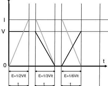
forms. Figure II-1 shows three possible linearized
transitions of voltage and current waveforms and how the energy of the transition is calculated.
These basic formulae are used in the following discussion. Further, they are important in understanding the effect of capacitance on turn off losses in a later section of this paper.
t V
I
0
E=1/2VIt E=1/3VIt E=1/6VIt
t t t
Figure II-1: Calculation of switching losses for various overlapping current and voltage waveforms
MOSFET switching losses have been extensively covered in [1]. We will review the switching losses caused by forced commutation of a diode.
If a diode is forced to turn off by another semiconductor switch, the diode will see switching losses. Additional losses will be generated in the semiconductor switch.
In simple terms, the reason for extra switching losses in a diode can be explained as follows. Figure II-2 shows the charge distributions for a diode in the conducting and the non-conducting states [2]. Here we are showing a p-n junction for illustrative
A-24 Fairchild Power Seminar 2007
purposes, rather than the p-i-n junction used in power diodes.
P-type N-type
x x=0
Minority carrier concentration near the junction
x
Minority carrier concentration near the junction
Electron concentration in P-type region Hole concentration in N-type region Electron concentration in P-type region Hole concentration in N-type region P-type N-type x=0
Diode conducting Diode blocking
Figure II-2: Charge distributions for a diode in the conducting and blocking states
For the diode to transition from the conducting to the non-conducting state, the charge distribution must change. This can only happen with a movement of charge, which is a flow of current. In some cases, such as a silicon carbide diode, the charge distribution difference is caused solely by the junction capacitance: again a movement of charge occurs when moving from the conducting to the non-conducting state.
The distribution curves show minority carrier density as a parameter. So, the larger the active junction area (other parameters being held constant), the larger the charge difference. Therefore devices in the same family with larger die sizes, represented by higher current ratings, will have a larger reverse recovery charge.
If the movement of charge between the non-conducting and non-conducting states happens during the same switch state, there is no additional loss. For example, in a discontinuous mode boost converter, the current in the diode drops to zero while the power switch is in the off state.
However, if an external switch forces the diode to change from the conducting to the non-conducting state (“forced commutation”) extra current is required to change the states, causing dissipation in both the diode and the switch.
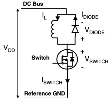
Figure II-3 and Figure II-4 show the reverse
recovery behavior of a diode under forced commutation. DC Bus Reference GND Switch
I
LI
DIODEI
SWITCHV
DDV
SWITCHV
DIODE+
+
-DC Bus Reference GND SwitchI
LI
DIODEI
SWITCHV
DDV
SWITCHV
DIODE+
+
-Figure II-3: Circuit to show the effect of diode reverse recovery on the diode and on the semiconductor switch
t iSWITCH VDD iDIODE IL 0 IL + IRRM IRRM -VDD vSWITCH vDIODE tA tB tR t iSWITCH VDD iDIODE IL 0 IL + IRRM IRRM -VDD vSWITCH vDIODE tA tB tR
Figure II-4: Effect of diode reverse recovery on the diode and on the semiconductor switch
The plot starts with the turn on of the lower switch. After the gate voltage on the lower switch reaches the Vth level, the lower switch builds up current in the saturation mode, causing a linear increase in the switch current, and a linear decrease in the diode current, as the inductor current is constant.
The diode temporarily conducts in the reverse
direction. The maximum current (IRRM) is the
reverse recovery current, and is specified in the diode datasheet. It increases greatly with temperature. It increases with di/dt. As will be shown later, it increases with current.
A-25 Fairchild Power Seminar 2007
Time interval tA is defined as the time between
the zero crossing of the current and the peak reverse
current. Time interval tB is defined as the time
between the peak of the reverse current and the time where the current falls to zero (or a pre-defined low level). The sum of tA and tB is called the reverse
recovery time, tRR.
The switching power dissipation in the diode is given by: RRM DD B DIODE ON t V I 6 1 E = (1)
where VDD is the bus voltage. The power
dissipation during time tA is considered to be part of
the conduction losses of the diode.
The reverse recovery current also induces extra losses in the semiconductor switch. The total switch on loss is given by the following formula:
B RRM L DD A RRM L DD R L DD SWITCH ON t I I V t I I V t I V E ) 3 1 2 1 ( ) 2 1 ( 2 1 + + + + = (2)
where IL is the load current and tR is the time
interval between the start of switching and when the semiconductor switch provides the full load current.
By setting tA and IRRM to zero, the equation for
on-losses in the absence of reverse recovery is readily obtained: B L DD R L DD SWITCH ON V I t V I t E ) 2 1 ( 2 1 + = (3)
where in this case tB is the time interval between
when the semiconductor switch provides the full load current and when the voltage across the switch has dropped to the minimum value.
The extra EON loss attributable to the diode can be
calculated by subtracting the two equations:
B RRM DD A RRM L DD EXTRA ON V I I t V I t E ) 3 1 ( ) 2 1 ( + + = (4)
Noting that IRRM can often exceed the normal
forward rated current of the diode, these extra switching losses and their impact are significant.
For a normal diode, tB is much smaller than tA.
For a soft recovery diode, tB is larger than tA. For a
given reverse recovery time, tRR (= tA + tB), the
equation above shows that the semiconductor switch losses when using a soft recovery diode are less than the losses caused by a normal diode, as:
RRM RRM L I I I 3 1 2 1 > + (5)
However, the switching loss generated in the diode itself (equation 1) is proportional to tB. As a
soft recovery diode has a larger tB value than a
normal diode, the diode losses will be higher. Nevertheless, accounting for these losses in the above equation shows that there is still a clear benefit for the overall system efficiency.
The important conclusion is that the use of a soft recovery diode will introduce more switch-on losses in the diode itself, but save additional losses in the semiconductor switch. When evaluating the performance of a new diode, it is therefore necessary to look at both the diode and semiconductor switch performance, not just the diode performance.
Another benefit of a soft switching diode is that
the dv/dt rate during time tB is much lower than for
a normal diode because tB is longer. High dv/dt can
cause ringing losses and extra EMI in a circuit. Finally, soft recovery diodes generally have a
lower IRRM than normal diodes.
In the absence of reverse recovery, equation (3) can be rearranged in terms of the applied di/dt and dv/dt in the system: dt dv V I 2 1 dt di I V 2 1 E 2 DD L 2 L DD SWITCH ON = + (6)
This equation will be used in later discussions. Finally, it is important to note the effect of
A-26 Fairchild Power Seminar 2007
temperature on IRRM and tRR. While the forward
voltage of a diode decreases as temperature increases, the parameters affecting switching
characteristics, IRRM and tRR, both increase with
temperature. With reference to Figure II-2, the
minority charge concentration will increase with
temperature, so it is to be expected that both IRRM
and tRR will also increase with temperature.
Figure II-5 demonstrates these results for two
industry standard diodes.
Results for Tj = 25°C
di/dt=200A/ms, Vdd=400V, If=8A, Tj=25°C Two industry standard diodes
Results for Tj = 125°C Results for Tj = 25°C
di/dt=200A/ms, Vdd=400V, If=8A, Tj=25°C Two industry standard diodes
Results for Tj = 125°C
Figure II-5: Comparison of reverse recovery performance for two industry standard diodes at Tj=25ºC and at Tj =125ºC. Upper curve: ISL9R860P2, lower curve: 8A/600V competitor part.
III. EXPERIMENTAL SETUP AND BASIC MEASUREMENTS
In principle, it is possible to estimate many of the factors affecting switching losses in a circuit. For
IGBT’s, EON and EOFF are normally specified in the
datasheet for a specific set of conditions. For MOSFET’s, these values can be calculated from the circuit parameters. The additional effect of the diode on switching losses can be estimated using the formulae from the previous section.
In practice, it is important to assess the performance in a real circuit. First, it is important to verify the performance compared with the theoretical framework. Second, effects which are difficult to quantify, such as the beneficial effect of node capacitance on the turn off performance, need to be considered.
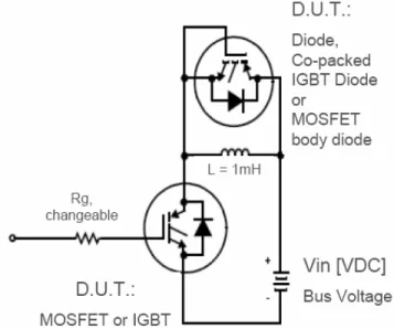
The objective of our experiments was to compare the performance of different types of diodes using one type of MOSFET. We chose diodes of all
speeds with ratings from 4A to 15A. All tests were performed at a current of 4A.
Figure III-1 shows the experimental setup. The
diode under test is on the high side. The MOSFET
(or IGBT) is on the low side. Figure III-2 shows the
waveforms needed to operate the circuit, taken when using an FQP9N50C MOSFET.
First, the MOSFET is turned on until the test current level in the inductor is reached. The MOSFET is then switched off, causing the test current to flow through the diode. Shortly afterwards, the MOSFET is switched on to measure the switch-on losses, and then switched off to measure the switch-off losses. As the MOSFET was only switched on for a very short time, the test results apply to a junction temperature close to the ambient room temperature of 25ºC.
The construction of the test set-up was on a standard prototype board having no copper plating. The devices under test were placed in sockets. The sockets were connected together with short, low impedance connections. The results obtained are comparable with those of a standard printed circuit board layout.
A-27 Fairchild Power Seminar 2007 Figure III-2: Drive waveforms for test circuit. Channel 1 is
the drain voltage, channel 2 is the gate voltage, and channel 4 is the drain current. MOSFET: FQP9N50C.
For slow di/dt testing we used a CD4000 series logic gate with external P-channel and N-channel MOSFET’s. In the course of the experiment, we found that the speed was insufficient for high speed testing, so we replaced the circuit with a 12V low voltage driver circuit (FAN5009) which has approximately 1 ohm output resistance when turning on.
Figure III-3: Waveforms measured during switch on
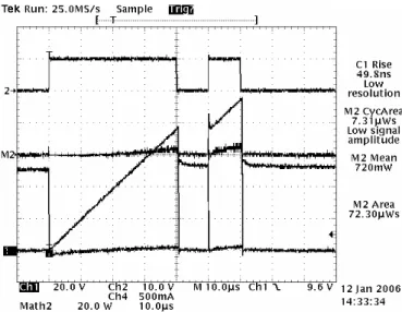
Figure III-3 shows a typical set of plots for EON
measurement. The parts used are the FQP9N50C MOSFET and the FFP08H60S diode. Channel 1 shows the voltage on the switching node. Before switching, the switching node voltage is high, here
300V. Channel 4 shows the current through the low side switch. When the MOSFET is switched on, the current rises with a di/dt influenced by the MOSFET gate charge characteristics and the driver circuit component values. Before switching, the current value is zero. After completion of switching, the current value is 4A in the example. The instantaneous power is calculated by the oscilloscope on Channel M2. The area under M2 represents the switching energy which in this case is 32.6 uJ (noting that 1W = 1J/s).
The maximum value of the current, minus the steady state current is equal to the reverse recovery current of the diode. In this case, this is 7.9A – 4A = 3.9A.
Figure III-4: Waveforms measured during turn off
Similarly, Figure III-4 shows a typical set of plots
for EOFF measurement. The turn-off transition is not
discussed in detail here because diode forward recovery, which occurs during turn-off, usually produces much smaller losses than reverse recovery during turn-on. Again, Channel 1 shows the voltage on the switching node, Channel 4 shows the current through the low side switch and Channel M2 shows the instantaneous power.
Note that there is a small level of ringing. Further, there is a small voltage spike caused by the forward recovery of the diode.
A-28 Fairchild Power Seminar 2007
IV. SWITCHING LOSS BEHAVIOR UNDER DIFFERENT TEST
CONDITIONS AND USING DIFFERENT DEVICES
In this section we review the effect of the diode on the switching losses seen during switch turn on. As the switching losses seen in the diode are much smaller, as discussed in Section II, these are not reviewed.
The first evaluation was to look at the effect of input voltage on the turn-on and turn-off losses. For the first stage of this experiment, we compared two diodes from the same family. The results are shown in Figure IV-1.
Eon and Eoff losses of the FET - FQP9N50C vs Input Voltage
0 5 10 15 20 25 30 35 40 45 50 0 50 100 150 200 250 300 350 Input Voltage [V] E on an d E o ff L o sses [u J] Eon @ ISL9R1560 Eoff @ ISL9R1560 Eon @ ISL9R460 Eoff @ ISL9R460
Figure IV-1: Comparison of EON and EOFF losses against voltage for 4A and 15A Stealth™ diodes
There are several important conclusions to be made. First, switching losses will always rise with input voltage. During the current ramp up phase, the losses are proportional to the product of the bus voltage and the load current, so a strong linear
relationship is to be expected. Second, the EON
losses are higher for a larger die device of the same family, than they are for a smaller die, or a lower
current rated device. Third, the EOFF losses are
lower for a larger device of the same family than they are for a smaller device. Finally, the EON losses
dominate, being approximately twice the EOFF
losses.
The next stage of the experiment was to compare
the EON losses for a greater variety of 600V diodes
rated in the range of 4A to 15A. Figure IV-2 shows
the results, followed by a table describing the part numbers.
Eon losses of the FET - FQP9N50C vs Input Voltage
0 10 20 30 40 50 60 70 80 90 0 50 100 150 200 250 300 350 Input Voltage [V] Eo n Lo s s e s [u J ] Eon @ MUR1560 Eon @ RURP860 Eon @ RURD660 Eon @ FFPF10UP60 Eon @ ISL9R1560 Eon @ RHRP860 Eon @ ISL9R860 Eon @ ISL9R460 Eon @ SIC 6A
Figure IV-2: EON losses versus voltage for a wide range of diodes
TABLEI
DIODESANDMOSFETBODYDIODESUSEDINTHEEVALUATION
Part Number Description
FCP11N60F Fast recovery diode from 11A, 600V superjunction MOSFET
FQP5N50CF Fast recovery diode from 5A, 500V planar MOSFET
MUR1560 15A, Ultrafast (low speed) 600V Diode RURP860 8A, Ultrafast (low speed) 600V Diode RURD660 6A, Ultrafast (low speed) 600V Diode FFPF10UP60 10A, Ultrafast (low speed) 600V Diode
ISL9R1560 15A, Stealth (soft, high speed) 600V Diode RHRP860 8A, Hyperfast (medium speed) 600V Diode ISL9R860 8A, Stealth (soft, high speed) 600V Diode ISL9R460 4A, Stealth (soft, high speed) 600V Diode
SiC 6A 6A, Silicon Carbide, 600V Diode
The lowest EON losses in the experiment came
from the silicon carbide and Stealth (highest speed) diodes. The Hyperfast (medium speed) diodes were next lowest, followed by the Ultrafast (lower speed) diodes. As predicted by theoretical analysis, for a given class of diodes, higher current rated devices (which have larger dies) had higher EON losses.
One interesting practical aspect is the effect of switching speed in this application. As discussed earlier, a certain amount of energy is needed to turn-on the semicturn-onductor switch:
A-29 Fairchild Power Seminar 2007 dt dv V I 2 1 dt di I V 2 1 E 2 DD L 2 L DD SWITCH ON = + (6 repeated)
At 160 A/us, 20000V/us, 300V and 4A, the EON
required just to turn-on the switch is 24uJ. With
reference to Figure IV-2 this accounts for a large
part of the losses for the best devices at 300V.
In many applications, the switching di/dt and dv/dt is limited by EMI constraints. Better efficiency can be obtained by using a faster switching diode, as the results show. However, at current prices, the incremental cost of moving to silicon carbide is very high. If system requirements limit di/dt to say 200A/us, from a switching perspective, silicon carbide diodes offer only a slight improvement in performance. For applications where much higher di/dt is permissible, silicon carbide diodes offer a definite benefit.
Another clear observation from the test results is that the benefit of a fast diode increases with voltage, shown by the increased spreading of the curves at higher voltage. The benefit of using a Stealth diode in a system using a 450V bus voltage is more than that at 300V.
The second evaluation was to look at the effect of input current on the turn-on and turn-off losses. For this experiment, we compared different diodes including MOSFET body diodes. The results are
shown in Figure IV-3
Eon and Eoff losses of the FET - FQP9N50C vs Current
0 20 40 60 80 100 120 140 160 180 200 0 1 2 3 4 5 6 7 Current [A] Eo n a n d E o ff Los s e s [u J] Eon @FCP11N60F Eon @ FQPF5N50CF Eon @ RURD660 Eon @ RHRP860 Eon @ ISL9R460 Eoff @ ISL9R460
Figure IV-3: Comparison of EON and EOFF losses against current for various diodes and for the body diodes in the FCP11N60F and FQPF5N50CF MOSFET’s
As expected from the theoretical analysis (equation 2), there is a strong linear dependence on the current. This results from the higher current flowing through the MOSFET. However, as will be shown shortly, the loss contribution from the diode is not strongly dependent on current for fast recovery diodes.
The third evaluation was to look at the effect of input current and input voltage on the maximum reverse recovery current. For this experiment, we compared different diodes including MOSFET body
diodes. The results are shown in Figure IV-4 and
Figure IV-5.
Irr, Reverse Recovery Peak Current of the Diode vs Current
0 2 4 6 8 10 12 14 0 1 2 3 4 5 6 7 Current [A] Re verse Reco ve ry Cu rren t [A] Irr @ FCP11N60F Irr @ FQPF5N50CF Irr @ RURD660 Irr @ RHRP860 Irr @ ISL9R460
Figure IV-4: Comparison of IRRM against load current for various diodes including MOSFET body diodes
A-30 Fairchild Power Seminar 2007
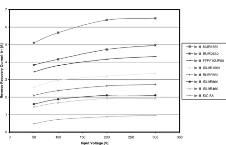
Irr, Reverse Recovery Peak Current of the Diode vs. Input Voltage
0 1 2 3 4 5 6 7 0 50 100 150 200 250 300 350 Input Voltage [V] Revers e R e co very Cu rren t I rr [ A ] Irr @ MUR1560 Irr @ RURD660 Irr @ FFPF10UP60 Irr @ ISL9R1560 Irr @ RHRP860 Irr @ ISL9R860 Irr @ ISL9R460 Irr @ SIC 6A
Figure IV-5: Comparison of IRRM against voltage for various diodes including MOSFET body diodes
Two important conclusions come out from the
experimental results. First, the IRRM level is not
strongly dependent on voltage and current for the faster diodes in the selection. We have seen in Section II that temperature has a larger effect. We will review the effect of di/dt shortly. Second, the reverse recovery current of fast recovery MOSFET’s is very high, even exceeding the nominal rated current of the devices.
The fourth evaluation was to look at the effect of di/dt. Increasing di/dt will reduce the turn-on losses in the MOSFET’s. However as a side effect, both IRRM and tRR will increase with increasing di/dt.
Reverse Recovery Current Irr of the Diode vs dI/dt @ V = 300V @ dI/dt = 4A
0 1 2 3 4 5 6 7 8 9 10 0 200 400 600 800 1000 1200 1400 1600 dI/dt [A/us] R everse Rec o v e ry C u rren t I rr [ A ] Eon @ ISL9R3060 Eon @ FFP08H60S Eon @ RHRP860 Eon @ ISL9R860 Eon @ ISL9R460
Figure IV-6: Effect of di/dt on reverse recovery current (IRRM)
Figure IV-6 shows the effect of di/dt on reverse
recovery current. Taking a simplified approach based on Figure II-4, the value 0.5tAIRRM is equal to
the reverse recovery charge for a hard switching diode, and IRRM/tA is equal to di/dt. So if the reverse
recovery charge remains constant, we would expect IRRM to increase with increasing di/dt, as seen in the
graph. A detailed analysis of the results shows that
IRRM increases more than expected from this
simplistic analysis. This is seen in datasheets as a higher reported reverse recovery charge for different di/dt conditions, other parameters being held the same.
So increasing di/dt will increase diode induced switching losses in the diode and in the semiconductor switch, and decrease switching losses caused by the overlap of the rising current and steady voltage waveforms. It is therefore important to assess which factor dominates.
Figure IV-7 shows the effect of increased di/dt on
EON losses. Here we see a clear benefit of higher
di/dt on EON losses despite the higher diode induced
switching losses. To get 400A/us, we used a 30 ohm gate resistor on the FQP9N50C driven by a FAN5009 1 ohm driver. For 600A/us we used FDD6N50C with a 30 ohm resistor. Values of 10 ohm and 3 ohm gave di/dt of 1400 A/us and 1600 A/us respectively.
Eon losses of the FET vs dI/dt @ V = 300V @ dI/dt = 4A
0 5 10 15 20 25 30 35 40 45 0 200 400 600 800 1000 1200 1400 1600 dI/dt [A/us] Eo n Lo s ses [ u J] Eon @ ISL9R3060 Eon @ FFP08H60S Eon @ RHRP860 Eon @ ISL9R860 Eon @ ISL9R460
A-31 Fairchild Power Seminar 2007
The final evaluation was to consider the effect of additional capacitance on the overall losses.
Figure IV-8: No capacitance: ISL9R460 diode, 300V, 4A
Figure IV-9: 470pF capacitance: ISL9R460, 300V, 4A
Figure IV-10: 1nF capacitance: ISL9R460, 300V, 4A
The figures show the different turn off curves for
a circuit with no parallel capacitance (Figure IV-8),
470pF parallel capacitance (Figure IV-9) and 1nF
parallel capacitance (Figure IV-10). As the
capacitance increases, EOFF decreases.
In the case of no parallel capacitance, the voltage rises before the current falls. With reference to
Figure II-1, the formula is 1/2VI for this case (26uJ
from the scope measurement). When 470pF is added, the voltage rises while the current is still falling, so the formula is 1/6VI, resulting in approximately 1/3 of the loss (8uJ). Further, the curves are smoother, moving away from the simple linearized approximation. In the final case, the overlap is very small (5uJ).
The addition of extra capacitance will cause a large increase in the turn-on losses. We show the 470nF turn-on example below:
Figure IV-11: 470pF capacitance: turn-on performance
If extra capacitance increases the EON losses but
reduces the EOFF losses, then there is the possibility
an optimum point. We conducted experiments with different capacitor values and came up with the
results in Figure IV-12. Based on these results, the
addition of a small amount of extra capacitance does indeed make sense for the particular configuration used. As it is difficult to quantitatively predict the effect of capacitance on
EOFF losses, such evaluation requires
A-32 Fairchild Power Seminar 2007
Eon and Eoff losses with a snubber Capacitance
0 10 20 30 40 50 60 70 80 90 100 0 100 200 300 400 500 600 700 800 900 1000
Capacitance parallel to the Diode [pF]
Et o t / Eo n / E o ff l o sses [u J] Etot at 300V Etot at 200V Etot at 100V Eoff at 300V Eon at 300V Eoff at 200V Eon at 200V Eoff at 100V Eon at 100V
Figure IV-12: Effect of adding parallel capacitance on EON, EOFF and total losses
V. PACKAGE RECOMMENDATIONS
The package size and type is an important parameter for the selection of diodes. While it is beyond the scope of this paper to cover detailed thermal design, we would like to cover a couple of points.
The maximum permissible junction temperature is always specified for power switches and diodes, and generally is 150ºC. In practice, designers will design to 125ºC maximum junction temperature to provide a safety margin for increased system robustness and reliability.
Combining this information with experience on how packages are used with heatsinks, we provide the following table as a guideline, for applications not using fans or forced convection:
Package and mounting Max Power
TO247 with isolated foil on heatsink 30W TO220 with isolated foil on heatsink 10W
TO263 on printed circuit board 1W
VI. CONCLUSION
Reverse recovery in diodes introduces small losses in the diode but larger losses in the MOSFET or IGBT which is switching the diode. These losses are influenced by the two reverse recovery parameters IRRM and tRR.
From a system design perspective, there are three aspects influencing the optimization of a half-bridge structure: di/dt, diode choice and the possible inclusion of a parallel capacitor.
Higher di/dt results in lower EON losses in the
circuits tested, noting that higher di/dt increases
IRRM losses less than it decreases the normal
switching losses. So from perspective of switch and diode losses, increasing di/dt is beneficial despite the increase in IRRM.
The use of fast recovery diodes improves switching losses, but generally worsens conduction losses. Larger current rated diodes of the same family have higher IRRM resulting in higher EON, and
a larger capacitance, resulting in lower EOFF.
Over-dimensioning of the diodes is not recommended as this leads to higher total switching losses.
Addition of extra capacitance increases EON losses
but decreases EOFF losses. There is the possibility
that an optimum total loss point will exist, meaning that the addition of extra capacitance will reduce total losses. Designers of circuits using half-bridges should consider this possibility in their applications: inclusion of a low cost capacitor may help improve efficiency.
REFERENCES
[1] J. P. Harper, “Understanding Modern Power MOSFET’s” Fairchild
Semiconductor Power Seminar 2006, www.fairchildsemi.com
[2] J. Millman, Microelectronics: Digital and Analog Circuits and
A-33 Fairchild Power Seminar 2007
Peter Haaf studied Elektrotechnik at the University of
Karlsruhe, Germany. After graduation in 1992, Peter joined the R&D department of Vossloh-Schwabe on power applications, becoming a design team leader. Since 2001, he has been a senior field application engineer for Fairchild Semiconductor in Germany focusing on power supply and high power applications.
Jon Harper After completing a BSc/MEng degree at the
University of Bath, England, Jon started as an applications engineer for microcontrollers at National Semiconductor in Germany. He completed an MBA degree at Warwick Business School in 1996 and joined the refounded Fairchild Semiconductor as a marketing engineer. Since 2002, Jon has covered technical marketing for industrial and white goods products, focusing on power electronics.