PIC16F84A
Data Sheet
18-pin Enhanced FLASH/EEPROM
8-bit Microcontroller
M
Information contained in this publication regarding device applications and the like is intended through suggestion only and may be superseded by updates. It is your responsibility to ensure that your application meets with your specifications. No representation or warranty is given and no liability is assumed by Microchip Technology Incorporated with respect to the accuracy or use of such information, or infringement of patents or other intellectual property rights arising from such use or otherwise. Use of Microchip’s products as critical com-ponents in life support systems is not authorized except with express written approval by Microchip. No licenses are con-veyed, implicitly or otherwise, under any intellectual property rights.
Trademarks
The Microchip name and logo, the Microchip logo, PIC, PICmicro, PICMASTER, PICSTART, PRO MATE, KEELOQ, SEEVAL, MPLAB and The Embedded Control Solutions Company are reg-istered trademarks of Microchip Technology Incorporated in the U.S.A. and other countries.
Total Endurance, ICSP, In-Circuit Serial Programming, Filter-Lab, MXDEV, microID, FlexROM, fuzzyLAB, MPASM, MPLINK, MPLIB, PICC, PICDEM, PICDEM.net, ICEPIC, Migratable Memory, FanSense, ECONOMONITOR, Select Mode and microPort are trademarks of Microchip Technology Incorporated in the U.S.A.
Serialized Quick Term Programming (SQTP) is a service mark of Microchip Technology Incorporated in the U.S.A.
All other trademarks mentioned herein are property of their respective companies.
© 2001, Microchip Technology Incorporated, Printed in the U.S.A., All Rights Reserved.
Printed on recycled paper.
Microchip received QS-9000 quality system certification for its worldwide headquarters, design and wafer fabrication facilities in Chandler and Tempe, Arizona in July 1999. The Company’s quality system processes and procedures are QS-9000 compliant for its PICmicro®8-bit MCUs, KEELOQ®code hopping
devices, Serial EEPROMs and microperipheral products. In addition, Microchip’s quality system for the design and manufacture of development systems is ISO 9001 certified. when used in the intended manner and under normal conditions.
• There are dishonest and possibly illegal methods used to breach the code protection feature. All of these methods, to our knowl-edge, require using the PICmicro microcontroller in a manner outside the operating specifications contained in the data sheet. The person doing so may be engaged in theft of intellectual property.
• Microchip is willing to work with the customer who is concerned about the integrity of their code.
• Neither Microchip nor any other semiconductor manufacturer can guarantee the security of their code. Code protection does not mean that we are guaranteeing the product as “unbreakable”.
• Code protection is constantly evolving. We at Microchip are committed to continuously improving the code protection features of our product.
M
PIC16F84A
High Performance RISC CPU Features:
• Only 35 single word instructions to learn • All instructions single-cycle except for program
branches which are two-cycle
• Operating speed: DC - 20 MHz clock input DC - 200 ns instruction cycle • 1024 words of program memory
• 68 bytes of Data RAM • 64 bytes of Data EEPROM • 14-bit wide instruction words • 8-bit wide data bytes
• 15 Special Function Hardware registers • Eight-level deep hardware stack
• Direct, indirect and relative addressing modes • Four interrupt sources:
- External RB0/INT pin - TMR0 timer overflow
- PORTB<7:4> interrupt-on-change - Data EEPROM write complete
Peripheral Features:
• 13 I/O pins with individual direction control • High current sink/source for direct LED drive
- 25 mA sink max. per pin - 25 mA source max. per pin • TMR0: 8-bit timer/counter with 8-bit
programmable prescaler
Special Microcontroller Features:
• 10,000 erase/write cycles Enhanced FLASH Program memory typical
• 10,000,000 typical erase/write cycles EEPROM Data memory typical
• EEPROM Data Retention > 40 years
• In-Circuit Serial Programming™ (ICSP™) - via two pins
• Power-on Reset (POR), Power-up Timer (PWRT), Oscillator Start-up Timer (OST)
• Watchdog Timer (WDT) with its own On-Chip RC Oscillator for reliable operation
Pin Diagrams
CMOS Enhanced FLASH/EEPROM
Technology:
• Low power, high speed technology • Fully static design
• Wide operating voltage range: - Commercial: 2.0V to 5.5V - Industrial: 2.0V to 5.5V • Low power consumption:
- < 2 mA typical @ 5V, 4 MHz - 15 µA typical @ 2V, 32 kHz
- < 0.5 µA typical standby current @ 2V RA1 RA0 OSC1/CLKIN OSC2/CLKOUT VDD RB7 RB6 RB5 RB4 RA2 RA3 RA4/T0CKI MCLR VSS RB0/INT RB1 RB2 RB3 •1 2 3 4 5 6 7 8 9 18 17 16 15 14 13 12 11 10 PDIP, SOIC PIC 16F 84A RA1 RA0 OSC1/CLKIN OSC2/CLKOUT VDD RB7 RB6 RB5 RB4 RA2 RA3 RA4/T0CKI MCLR VSS RB0/INT RB1 RB2 RB3 •1 2 3 4 5 6 7 8 9 20 19 18 17 16 15 14 13 12 SSOP PIC16 F 84 A 10 11 VSS VDD
Table of Contents
1.0 Device Overview ... 3
2.0 Memory Organization ... 5
3.0 Data EEPROM Memory ... 13
4.0 I/O Ports ... 15
5.0 Timer0 Module ... 19
6.0 Special Features of the CPU ... 21
7.0 Instruction Set Summary ... 35
8.0 Development Support... 43
9.0 Electrical Characteristics ... 49
10.0 DC/AC Characteristic Graphs ... 61
11.0 Packaging Information... 71
Appendix A: Revision History ... 75
Appendix B: Conversion Considerations... 76
Appendix C: Migration from Baseline to Mid-Range Devices ... 78
Index ... 79
On-Line Support... 83
Reader Response ... 84
PIC16F84A Product Identification System ... 85
TO OUR VALUED CUSTOMERS
It is our intention to provide our valued customers with the best documentation possible to ensure successful use of your Microchip products. To this end, we will continue to improve our publications to better suit your needs. Our publications will be refined and enhanced as new volumes and updates are introduced.
If you have any questions or comments regarding this publication, please contact the Marketing Communications Department via E-mail at [email protected] or fax the Reader Response Form in the back of this data sheet to (480) 792-4150. We welcome your feedback.
Most Current Data Sheet
To obtain the most up-to-date version of this data sheet, please register at our Worldwide Web site at: http://www.microchip.com
You can determine the version of a data sheet by examining its literature number found on the bottom outside corner of any page. The last character of the literature number is the version number, (e.g., DS30000A is version A of document DS30000).
Errata
An errata sheet, describing minor operational differences from the data sheet and recommended workarounds, may exist for current devices. As device/documentation issues become known to us, we will publish an errata sheet. The errata will specify the revision of silicon and revision of document to which it applies.
To determine if an errata sheet exists for a particular device, please check with one of the following: • Microchip’s Worldwide Web site; http://www.microchip.com
• Your local Microchip sales office (see last page)
• The Microchip Corporate Literature Center; U.S. FAX: (480) 792-7277
When contacting a sales office or the literature center, please specify which device, revision of silicon and data sheet (include liter-ature number) you are using.
Customer Notification System
1.0
DEVICE OVERVIEW
This document contains device specific information for the operation of the PIC16F84A device. Additional information may be found in the PICmicro™ Mid-Range Reference Manual, (DS33023), which may be downloaded from the Microchip website. The Refer-ence Manual should be considered a complementary document to this data sheet, and is highly recom-mended reading for a better understanding of the device architecture and operation of the peripheral modules.
The PIC16F84A belongs to the mid-range family of the PICmicro® microcontroller devices. A block diagram of the device is shown in Figure 1-1.
The program memory contains 1K words, which trans-lates to 1024 instructions, since each 14-bit program memory word is the same width as each device instruc-tion. The data memory (RAM) contains 68 bytes. Data EEPROM is 64 bytes.
There are also 13 I/O pins that are user-configured on a pin-to-pin basis. Some pins are multiplexed with other device functions. These functions include:
• External interrupt
• Change on PORTB interrupt • Timer0 clock input
Table 1-1 details the pinout of the device with descrip-tions and details for each pin.
FIGURE 1-1: PIC16F84A BLOCK DIAGRAM
FLASH Program Memory
Program Counter 13
Program Bus
Instruction Register
8 Level Stack (13-bit)
Direct Addr
8
Instruction Decode & Control
Timing Generation
OSC2/CLKOUT OSC1/CLKIN
Power-up Timer Oscillator Start-up Timer
Power-on Reset Watchdog
Timer
MCLR VDD, VSS
W reg ALU
MUX
I/O Ports TMR0
STATUS reg FSR reg
Indirect Addr
RA3:RA0 RB7:RB1 RA4/T0CKI EEADR EEPROM Data Memory
64 x 8 EEDATA
Addr Mux
RAM Addr RAM
File Registers
EEPROM Data Memory Data Bus
5
7
7
RB0/INT 14
8
8 1K x 14
TABLE 1-1: PIC16F84A PINOUT DESCRIPTION
Pin Name PDIP
No.
SOIC No.
SSOP No.
I/O/P Type
Buffer
Type Description
OSC1/CLKIN 16 16 18 I ST/CMOS(3) Oscillator crystal input/external clock source input.
OSC2/CLKOUT 15 15 19 O — Oscillator crystal output. Connects to crystal or
resonator in Crystal Oscillator mode. In RC mode, OSC2 pin outputs CLKOUT, which has 1/4 the frequency of OSC1 and denotes the instruction cycle rate.
MCLR 4 4 4 I/P ST Master Clear (Reset) input/programming voltage
input. This pin is an active low RESET to the device. PORTA is a bi-directional I/O port.
RA0 17 17 19 I/O TTL
RA1 18 18 20 I/O TTL
RA2 1 1 1 I/O TTL
RA3 2 2 2 I/O TTL
RA4/T0CKI 3 3 3 I/O ST Can also be selected to be the clock input to the
TMR0 timer/counter. Output is open drain type. PORTB is a bi-directional I/O port. PORTB can be software programmed for internal weak pull-up on all inputs.
RB0/INT 6 6 7 I/O TTL/ST(1) RB0/INT can also be selected as an external
interrupt pin.
RB1 7 7 8 I/O TTL
RB2 8 8 9 I/O TTL
RB3 9 9 10 I/O TTL
RB4 10 10 11 I/O TTL Interrupt-on-change pin.
RB5 11 11 12 I/O TTL Interrupt-on-change pin.
RB6 12 12 13 I/O TTL/ST(2) Interrupt-on-change pin.
Serial programming clock.
RB7 13 13 14 I/O TTL/ST(2) Interrupt-on-change pin.
Serial programming data.
VSS 5 5 5,6 P — Ground reference for logic and I/O pins.
VDD 14 14 15,16 P — Positive supply for logic and I/O pins.
Legend: I= input O = Output I/O = Input/Output P = Power
— = Not used TTL = TTL input ST = Schmitt Trigger input Note 1: This buffer is a Schmitt Trigger input when configured as the external interrupt.
2: This buffer is a Schmitt Trigger input when used in Serial Programming mode.
2.0
MEMORY ORGANIZATION
There are two memory blocks in the PIC16F84A. These are the program memory and the data memory. Each block has its own bus, so that access to each block can occur during the same oscillator cycle. The data memory can further be broken down into the general purpose RAM and the Special Function Registers (SFRs). The operation of the SFRs that control the “core” are described here. The SFRs used to control the peripheral modules are described in the section discussing each individual peripheral module. The data memory area also contains the data EEPROM memory. This memory is not directly mapped into the data memory, but is indirectly mapped. That is, an indirect address pointer specifies the address of the data EEPROM memory to read/write. The 64 bytes of data EEPROM memory have the address range 0h-3Fh. More details on the EEPROM memory can be found in Section 3.0.
Additional information on device memory may be found in the PICmicro™ Mid-Range Reference Manual, (DS33023).
2.1
Program Memory Organization
The PIC16FXX has a 13-bit program counter capable of addressing an 8K x 14 program memory space. For the PIC16F84A, the first 1K x 14 (0000h-03FFh) are physically implemented (Figure 2-1). Accessing a loca-tion above the physically implemented address will cause a wraparound. For example, for locations 20h, 420h, 820h, C20h, 1020h, 1420h, 1820h, and 1C20h, the instruction will be the same.
The RESET vector is at 0000h and the interrupt vector is at 0004h.
FIGURE 2-1: PROGRAM MEMORY MAP
AND STACK - PIC16F84A PC<12:0>
Stack Level 1 • Stack Level 8 RESET Vector Peripheral Interrupt Vector
• •
Us
er M
e
mor
y
Sp
ac
e
CALL, RETURN RETFIE, RETLW
13
0000h
0004h
1FFFh 3FFh
2.2
Data Memory Organization
The data memory is partitioned into two areas. The first is the Special Function Registers (SFR) area, while the second is the General Purpose Registers (GPR) area. The SFRs control the operation of the device.
Portions of data memory are banked. This is for both the SFR area and the GPR area. The GPR area is banked to allow greater than 116 bytes of general purpose RAM. The banked areas of the SFR are for the registers that control the peripheral functions. Banking requires the use of control bits for bank selection. These control bits are located in the STATUS Register. Figure 2-2 shows the data memory map organization. Instructions MOVWF and MOVF can move values from the W register to any location in the register file (“F”), and vice-versa.
The entire data memory can be accessed either directly using the absolute address of each register file or indirectly through the File Select Register (FSR) (Section 2.5). Indirect addressing uses the present value of the RP0 bit for access into the banked areas of data memory.
Data memory is partitioned into two banks which contain the general purpose registers and the special function registers. Bank 0 is selected by clearing the RP0 bit (STATUS<5>). Setting the RP0 bit selects Bank 1. Each Bank extends up to 7Fh (128 bytes). The first twelve locations of each Bank are reserved for the Special Function Registers. The remainder are Gen-eral Purpose Registers, implemented as static RAM.
2.2.1 GENERAL PURPOSE REGISTER
FILE
Each General Purpose Register (GPR) is 8-bits wide and is accessed either directly or indirectly through the FSR (Section 2.5).
The GPR addresses in Bank 1 are mapped to addresses in Bank 0. As an example, addressing loca-tion 0Ch or 8Ch will access the same GPR.
FIGURE 2-2: REGISTER FILE MAP -
PIC16F84A File Address
00h 01h 02h 03h 04h 05h 06h 07h 08h 09h 0Ah 0Bh 0Ch
7Fh
80h 81h 82h 83h 84h 85h 86h 87h 88h 89h 8Ah 8Bh 8Ch
FFh
Bank 0 Bank 1
Indirect addr.(1) Indirect addr.(1)
TMR0 OPTION_REG
PCL STATUS
FSR PORTA PORTB
EEDATA EEADR PCLATH INTCON
68 General Purpose Registers
(SRAM)
PCL STATUS
FSR TRISA TRISB
EECON1 EECON2(1)
PCLATH INTCON
Mapped in Bank 0
Unimplemented data memory location, read as ’0’. File Address
Note 1: Not a physical register.
CFh D0h 4Fh
50h
(accesses)
2.3
Special Function Registers
The Special Function Registers (Figure 2-2 and Table 2-1) are used by the CPU and Peripheral functions to control the device operation. These registers are static RAM.
The special function registers can be classified into two sets, core and peripheral. Those associated with the core functions are described in this section. Those related to the operation of the peripheral features are described in the section for that specific feature.
TABLE 2-1: SPECIAL FUNCTION REGISTER FILE SUMMARY
Addr Name Bit 7 Bit 6 Bit 5 Bit 4 Bit 3 Bit 2 Bit 1 Bit 0
Value on Power-on RESET
Details on page Bank 0
00h INDF Uses contents of FSR to address Data Memory (not a physical register) ---- ---- 11
01h TMR0 8-bit Real-Time Clock/Counter xxxx xxxx 20
02h PCL Low Order 8 bits of the Program Counter (PC) 0000 0000 11
03h STATUS(2) IRP RP1 RP0 TO PD Z DC C 0001 1xxx 8
04h FSR Indirect Data Memory Address Pointer 0 xxxx xxxx 11
05h PORTA(4) — — — RA4/T0CKI RA3 RA2 RA1 RA0 ---x xxxx 16
06h PORTB(5) RB7 RB6 RB5 RB4 RB3 RB2 RB1 RB0/INT xxxx xxxx 18
07h — Unimplemented location, read as '0' — —
08h EEDATA EEPROM Data Register xxxx xxxx 13,14
09h EEADR EEPROM Address Register xxxx xxxx 13,14
0Ah PCLATH — — — Write Buffer for upper 5 bits of the PC(1) ---0 0000 11
0Bh INTCON GIE EEIE T0IE INTE RBIE T0IF INTF RBIF 0000 000x 10
Bank 1
80h INDF Uses Contents of FSR to address Data Memory (not a physical register) ---- ---- 11
81h OPTION_REG RBPU INTEDG T0CS T0SE PSA PS2 PS1 PS0 1111 1111 9
82h PCL Low order 8 bits of Program Counter (PC) 0000 0000 11
83h STATUS (2) IRP RP1 RP0 TO PD Z DC C 0001 1xxx 8
84h FSR Indirect data memory address pointer 0 xxxx xxxx 11
85h TRISA — — — PORTA Data Direction Register ---1 1111 16
86h TRISB PORTB Data Direction Register 1111 1111 18
87h — Unimplemented location, read as '0' — —
88h EECON1 — — — EEIF WRERR WREN WR RD ---0 x000 13
89h EECON2 EEPROM Control Register 2 (not a physical register) ---- ---- 14
0Ah PCLATH — — — Write buffer for upper 5 bits of the PC(1) ---0 0000 11
0Bh INTCON GIE EEIE T0IE INTE RBIE T0IF INTF RBIF 0000 000x 10
Legend: x = unknown, u = unchanged. - = unimplemented, read as '0', q = value depends on condition
Note 1: The upper byte of the program counter is not directly accessible. PCLATH is a slave register for PC<12:8>. The contents of PCLATH can be transferred to the upper byte of the program counter, but the contents of PC<12:8> are never trans-ferred to PCLATH.
2: The TO and PD status bits in the STATUS register are not affected by a MCLR Reset.
3: Other (non power-up) RESETS include: external RESET through MCLR and the Watchdog Timer Reset. 4: On any device RESET, these pins are configured as inputs.
2.3.1 STATUS REGISTER
The STATUS register contains the arithmetic status of the ALU, the RESET status and the bank select bit for data memory.
As with any register, the STATUS register can be the destination for any instruction. If the STATUS register is the destination for an instruction that affects the Z, DC or C bits, then the write to these three bits is disabled. These bits are set or cleared according to device logic. Furthermore, the TO and PD bits are not writable. Therefore, the result of an instruction with the STATUS register as destination may be different than intended. For example, CLRF STATUS will clear the upper three bits and set the Z bit. This leaves the STATUS register
as 000u u1uu (where u = unchanged).
Only the BCF, BSF, SWAPF and MOVWF instructions should be used to alter the STATUS register (Table 7-2), because these instructions do not affect any status bit.
REGISTER 2-1: STATUS REGISTER (ADDRESS 03h, 83h)
Note 1: The IRP and RP1 bits (STATUS<7:6>) are not used by the PIC16F84A and should be programmed as cleared. Use of these bits as general purpose R/W bits is NOT recommended, since this may affect upward compatibility with future products. 2: The C and DC bits operate as a borrow and digit borrow out bit, respectively, in subtraction. See the SUBLW and SUBWF
instructions for examples.
3: When the STATUS register is the destination for an instruction that affects the Z, DC or C bits, then the write to these three bits is disabled. The specified bit(s) will be updated according to device logic
R/W-0 R/W-0 R/W-0 R-1 R-1 R/W-x R/W-x R/W-x
IRP RP1 RP0 TO PD Z DC C
bit 7 bit 0
bit 7-6 Unimplemented: Maintain as ‘0’
bit 5 RP0: Register Bank Select bits (used for direct addressing) 01 = Bank 1 (80h - FFh)
00 = Bank 0 (00h - 7Fh) bit 4 TO: Time-out bit
1 = After power-up, CLRWDT instruction, or SLEEP instruction
0 = A WDT time-out occurred bit 3 PD: Power-down bit
1 = After power-up or by the CLRWDT instruction
0 = By execution of the SLEEP instruction bit 2 Z: Zero bit
1 = The result of an arithmetic or logic operation is zero
0 = The result of an arithmetic or logic operation is not zero
bit 1 DC: Digit carry/borrow bit (ADDWF, ADDLW,SUBLW,SUBWF instructions) (for borrow, the polarity is reversed)
1 = A carry-out from the 4th low order bit of the result occurred
0 = No carry-out from the 4th low order bit of the result
bit 0 C: Carry/borrow bit (ADDWF, ADDLW,SUBLW,SUBWF instructions) (for borrow, the polarity is reversed)
1 = A carry-out from the Most Significant bit of the result occurred
0 = No carry-out from the Most Significant bit of the result occurred
Note: A subtraction is executed by adding the two’s complement of the second operand. For rotate (RRF, RLF) instructions, this bit is loaded with either the high or low order bit of the source register.
Legend:
R = Readable bit W = Writable bit U = Unimplemented bit, read as ‘0’ - n = Value at POR ’1’ = Bit is set ’0’ = Bit is cleared x = Bit is unknown
2.3.2 OPTION REGISTER
The OPTION register is a readable and writable register which contains various control bits to configure the TMR0/WDT prescaler, the external INT interrupt, TMR0, and the weak pull-ups on PORTB.
REGISTER 2-2: OPTION REGISTER (ADDRESS 81h)
Note: When the prescaler is assigned to
the WDT (PSA = ’1’), TMR0 has a 1:1 prescaler assignment.
R/W-1 R/W-1 R/W-1 R/W-1 R/W-1 R/W-1 R/W-1 R/W-1
RBPU INTEDG T0CS T0SE PSA PS2 PS1 PS0
bit 7 bit 0
bit 7 RBPU: PORTB Pull-up Enable bit 1 = PORTB pull-ups are disabled
0 = PORTB pull-ups are enabled by individual port latch values bit 6 INTEDG: Interrupt Edge Select bit
1 = Interrupt on rising edge of RB0/INT pin
0 = Interrupt on falling edge of RB0/INT pin bit 5 T0CS: TMR0 Clock Source Select bit
1 = Transition on RA4/T0CKI pin
0 = Internal instruction cycle clock (CLKOUT) bit 4 T0SE: TMR0 Source Edge Select bit
1 = Increment on high-to-low transition on RA4/T0CKI pin
0 = Increment on low-to-high transition on RA4/T0CKI pin bit 3 PSA: Prescaler Assignment bit
1 = Prescaler is assigned to the WDT
0 = Prescaler is assigned to the Timer0 module bit 2-0 PS2:PS0: Prescaler Rate Select bits
Legend:
R = Readable bit W = Writable bit U = Unimplemented bit, read as ‘0’ - n = Value at POR ’1’ = Bit is set ’0’ = Bit is cleared x = Bit is unknown
000 001 010 011 100 101 110 111
1 : 2 1 : 4 1 : 8 1 : 16 1 : 32 1 : 64 1 : 128 1 : 256
1 : 1 1 : 2 1 : 4 1 : 8 1 : 16 1 : 32 1 : 64 1 : 128 Bit Value TMR0 Rate WDT Rate
2.3.3 INTCON REGISTER
The INTCON register is a readable and writable register that contains the various enable bits for all interrupt sources.
REGISTER 2-3: INTCON REGISTER (ADDRESS 0Bh, 8Bh)
Note: Interrupt flag bits are set when an interrupt condition occurs, regardless of the state of its corresponding enable bit or the global enable bit, GIE (INTCON<7>).
R/W-0 R/W-0 R/W-0 R/W-0 R/W-0 R/W-0 R/W-0 R/W-x
GIE EEIE T0IE INTE RBIE T0IF INTF RBIF
bit 7 bit 0
bit 7 GIE: Global Interrupt Enable bit 1 = Enables all unmasked interrupts
0 = Disables all interrupts
bit 6 EEIE: EE Write Complete Interrupt Enable bit 1 = Enables the EE Write Complete interrupts
0 = Disables the EE Write Complete interrupt bit 5 T0IE: TMR0 Overflow Interrupt Enable bit
1 = Enables the TMR0 interrupt
0 = Disables the TMR0 interrupt
bit 4 INTE: RB0/INT External Interrupt Enable bit 1 = Enables the RB0/INT external interrupt
0 = Disables the RB0/INT external interrupt bit 3 RBIE: RB Port Change Interrupt Enable bit
1 = Enables the RB port change interrupt
0 = Disables the RB port change interrupt bit 2 T0IF: TMR0 Overflow Interrupt Flag bit
1 = TMR0 register has overflowed (must be cleared in software)
0 = TMR0 register did not overflow bit 1 INTF: RB0/INT External Interrupt Flag bit
1 = The RB0/INT external interrupt occurred (must be cleared in software)
0 = The RB0/INT external interrupt did not occur bit 0 RBIF: RB Port Change Interrupt Flag bit
1 = At least one of the RB7:RB4 pins changed state (must be cleared in software)
0 = None of the RB7:RB4 pins have changed state
Legend:
R = Readable bit W = Writable bit U = Unimplemented bit, read as ‘0’ - n = Value at POR ’1’ = Bit is set ’0’ = Bit is cleared x = Bit is unknown
2.4
PCL and PCLATH
The program counter (PC) specifies the address of the instruction to fetch for execution. The PC is 13 bits wide. The low byte is called the PCL register. This reg-ister is readable and writable. The high byte is called the PCH register. This register contains the PC<12:8> bits and is not directly readable or writable. If the pro-gram counter (PC) is modified or a conditional test is true, the instruction requires two cycles. The second cycle is executed as a NOP. All updates to the PCH reg-ister go through the PCLATH regreg-ister.
2.4.1 STACK
The stack allows a combination of up to 8 program calls and interrupts to occur. The stack contains the return address from this branch in program execution. Mid-range devices have an 8 level deep x 13-bit wide hardware stack. The stack space is not part of either program or data space and the stack pointer is not readable or writable. The PC is PUSHed onto the stack when a CALL instruction is executed or an interrupt causes a branch. The stack is POPed in the event of a
RETURN, RETLW or a RETFIE instruction execution.
PCLATH is not modified when the stack is PUSHed or POPed.
After the stack has been PUSHed eight times, the ninth push overwrites the value that was stored from the first push. The tenth push overwrites the second push (and so on).
2.5
Indirect Addressing; INDF and
FSR Registers
The INDF register is not a physical register. Addressing INDF actually addresses the register whose address is contained in the FSR register (FSR is a pointer). This is indirect addressing.
EXAMPLE 2-1: INDIRECT ADDRESSING
Reading INDF itself indirectly (FSR = 0) will produce 00h. Writing to the INDF register indirectly results in a no-operation (although STATUS bits may be affected). A simple program to clear RAM locations 20h-2Fh using indirect addressing is shown in Example 2-2.
EXAMPLE 2-2: HOW TO CLEAR RAM
USING INDIRECT ADDRESSING
An effective 9-bit address is obtained by concatenating the 8-bit FSR register and the IRP bit (STATUS<7>), as shown in Figure 2-3. However, IRP is not used in the PIC16F84A.
• Register file 05 contains the value 10h • Register file 06 contains the value 0Ah • Load the value 05 into the FSR register • A read of the INDF register will return the value
of 10h
• Increment the value of the FSR register by one (FSR = 06)
• A read of the INDF register now will return the value of 0Ah.
movlw 0x20 ;initialize pointer movwf FSR ;to RAM
NEXT clrf INDF ;clear INDF register incf FSR ;inc pointer
btfss FSR,4 ;all done? goto NEXT ;NO, clear next CONTINUE
FIGURE 2-3: DIRECT/INDIRECT ADDRESSING Direct Addressing
RP1 RP0 6 From Opcode 0 IRP 7 (FSR) 0
Indirect Addressing
Bank Select Location Select Bank Select Location Select
00 01
80h
FFh 00h
0Bh 0Ch
7Fh
Bank 0 Bank 1
Note 1: For memory map detail, see Figure 2-2.
2: Maintain as clear for upward compatibility with future products. 3: Not implemented.
4Fh 50h Data
Memory(1)
(3) (3)
(2) (2)
Addresses map back to Bank 0
3.0
DATA EEPROM MEMORY
The EEPROM data memory is readable and writable during normal operation (full VDD range). This memory is not directly mapped in the register file space. Instead it is indirectly addressed through the Special Function Registers. There are four SFRs used to read and write this memory. These registers are:
• EECON1
• EECON2 (not a physically implemented register) • EEDATA
• EEADR
EEDATA holds the 8-bit data for read/write, and EEADR holds the address of the EEPROM location being accessed. PIC16F84A devices have 64 bytes of data EEPROM with an address range from 0h to 3Fh.
The EEPROM data memory allows byte read and write. A byte write automatically erases the location and writes the new data (erase before write). The EEPROM data memory is rated for high erase/write cycles. The write time is controlled by an on-chip timer. The write-time will vary with voltage and temperature as well as from chip to chip. Please refer to AC specifications for exact limits.
When the device is code protected, the CPU may continue to read and write the data EEPROM memory. The device programmer can no longer access this memory.
Additional information on the Data EEPROM is avail-able in the PICmicro™ Mid-Range Reference Manual (DS33023).
REGISTER 3-1: EECON1 REGISTER (ADDRESS 88h)
U-0 U-0 U-0 R/W-0 R/W-x R/W-0 R/S-0 R/S-0
— — — EEIF WRERR WREN WR RD
bit 7 bit 0
bit 7-5 Unimplemented: Read as '0'
bit 4 EEIF: EEPROM Write Operation Interrupt Flag bit
1 = The write operation completed (must be cleared in software)
0 = The write operation is not complete or has not been started bit 3 WRERR: EEPROM Error Flag bit
1 = A write operation is prematurely terminated
(any MCLR Reset or any WDT Reset during normal operation)
0 = The write operation completed bit 2 WREN: EEPROM Write Enable bit
1 = Allows write cycles
0 = Inhibits write to the EEPROM bit 1 WR: Write Control bit
1 = Initiates a write cycle. The bit is cleared by hardware once write is complete. The WR bit can only be set (not cleared) in software.
0 = Write cycle to the EEPROM is complete bit 0 RD: Read Control bit
1 = Initiates an EEPROM read RD is cleared in hardware. The RD bit can only be set (not cleared) in software.
0 = Does not initiate an EEPROM read
Legend:
R = Readable bit W = Writable bit U = Unimplemented bit, read as ‘0’ - n = Value at POR ’1’ = Bit is set ’0’ = Bit is cleared x = Bit is unknown
3.1
Reading the EEPROM Data
Memory
To read a data memory location, the user must write the address to the EEADR register and then set control bit RD (EECON1<0>). The data is available, in the very next cycle, in the EEDATA register; therefore, it can be read in the next instruction. EEDATA will hold this value until another read or until it is written to by the user (during a write operation).
EXAMPLE 3-1: DATA EEPROM READ
3.2
Writing to the EEPROM Data
Memory
To write an EEPROM data location, the user must first write the address to the EEADR register and the data to the EEDATA register. Then the user must follow a specific sequence to initiate the write for each byte.
EXAMPLE 3-2: DATA EEPROM WRITE
The write will not initiate if the above sequence is not exactly followed (write 55h to EECON2, write AAh to EECON2, then set WR bit) for each byte. We strongly recommend that interrupts be disabled during this code segment.
Additionally, the WREN bit in EECON1 must be set to enable write. This mechanism prevents accidental writes to data EEPROM due to errant (unexpected) code exe-cution (i.e., lost programs). The user should keep the WREN bit clear at all times, except when updating EEPROM. The WREN bit is not cleared by hardware. After a write sequence has been initiated, clearing the WREN bit will not affect this write cycle. The WR bit will be inhibited from being set unless the WREN bit is set. At the completion of the write cycle, the WR bit is cleared in hardware and the EE Write Complete Interrupt Flag bit (EEIF) is set. The user can either enable this interrupt or poll this bit. EEIF must be cleared by software.
3.3
Write Verify
Depending on the application, good programming practice may dictate that the value written to the Data EEPROM should be verified (Example 3-3) to the desired value to be written. This should be used in applications where an EEPROM bit will be stressed near the specification limit.
Generally, the EEPROM write failure will be a bit which was written as a ’0’, but reads back as a ’1’ (due to leakage off the bit).
EXAMPLE 3-3: WRITE VERIFY
TABLE 3-1: REGISTERS/BITS ASSOCIATED WITH DATA EEPROM
BCF STATUS, RP0 ; Bank 0 MOVLW CONFIG_ADDR ;
MOVWF EEADR ; Address to read BSF STATUS, RP0 ; Bank 1
BSF EECON1, RD ; EE Read BCF STATUS, RP0 ; Bank 0 MOVF EEDATA, W ; W = EEDATA
BSF STATUS, RP0 ; Bank 1 BCF INTCON, GIE ; Disable INTs. BSF EECON1, WREN ; Enable Write MOVLW 55h ;
MOVWF EECON2 ; Write 55h MOVLW AAh ;
MOVWF EECON2 ; Write AAh BSF EECON1,WR ; Set WR bit ; begin write BSF INTCON, GIE ; Enable INTs.
R e qu ir ed S e qu en c e
BCF STATUS,RP0 ; Bank 0
: ; Any code
: ; can go here
MOVF EEDATA,W ; Must be in Bank 0 BSF STATUS,RP0 ; Bank 1
READ
BSF EECON1, RD ; YES, Read the ; value written BCF STATUS, RP0 ; Bank 0
;
; Is the value written ; (in W reg) and ; read (in EEDATA) ; the same?
; SUBWF EEDATA, W ;
BTFSS STATUS, Z ; Is difference 0? GOTO WRITE_ERR ; NO, Write error
Address Name Bit 7 Bit 6 Bit 5 Bit 4 Bit 3 Bit 2 Bit 1 Bit 0
Value on Power-on Reset Value on all other RESETS
08h EEDATA EEPROM Data Register xxxx xxxx uuuu uuuu
09h EEADR EEPROM Address Register xxxx xxxx uuuu uuuu
88h EECON1 — — — EEIF WRERR WREN WR RD ---0 x000 ---0 q000
89h EECON2 EEPROM Control Register 2 ---- ----
----Legend: x = unknown, u = unchanged, - = unimplemented, read as '0', q = value depends upon condition. Shaded cells are not used by data EEPROM.
4.0
I/O PORTS
Some pins for these I/O ports are multiplexed with an alternate function for the peripheral features on the device. In general, when a peripheral is enabled, that pin may not be used as a general purpose I/O pin. Additional information on I/O ports may be found in the PICmicro™ Mid-Range Reference Manual (DS33023).
4.1
PORTA and TRISA Registers
PORTA is a 5-bit wide, bi-directional port. The corre-sponding data direction register is TRISA. Setting a TRISA bit (= 1) will make the corresponding PORTA pin an input (i.e., put the corresponding output driver in a Hi-Impedance mode). Clearing a TRISA bit (= 0) will make the corresponding PORTA pin an output (i.e., put the contents of the output latch on the selected pin).
Reading the PORTA register reads the status of the pins, whereas writing to it will write to the port latch. All write operations are read-modify-write operations. Therefore, a write to a port implies that the port pins are read. This value is modified and then written to the port data latch.
Pin RA4 is multiplexed with the Timer0 module clock input to become the RA4/T0CKI pin. The RA4/T0CKI pin is a Schmitt Trigger input and an open drain output. All other RA port pins have TTL input levels and full CMOS output drivers.
EXAMPLE 4-1: INITIALIZING PORTA
FIGURE 4-1: BLOCK DIAGRAM OF
PINS RA3:RA0
FIGURE 4-2: BLOCK DIAGRAM OF PIN
RA4 Note: On a Power-on Reset, these pins are
con-figured as inputs and read as '0'.
BCF STATUS, RP0 ;
CLRF PORTA ; Initialize PORTA by ; clearing output ; data latches BSF STATUS, RP0 ; Select Bank 1
MOVLW 0x0F ; Value used to
; initialize data ; direction
MOVWF TRISA ; Set RA<3:0> as inputs ; RA4 as output
; TRISA<7:5> are always ; read as ’0’.
Data Bus
Q D
Q CK
Q D
Q CK
Q D
EN P
N WR
Port
WR TRIS
Data Latch
TRIS Latch
RD TRIS
RD Port
TTL Input Buffer
VSS VDD
I/O pin
Note: I/O pins have protection diodes to VDD and VSS.
Data Bus WR Port
WR TRIS
RD Port
Data Latch
TRIS Latch
RD TRIS
Schmitt Trigger Input Buffer
N VSS
RA4 pin Q
D
Q CK
Q D
Q CK
EN
Q D
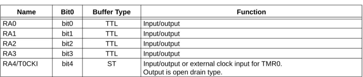
TABLE 4-1: PORTA FUNCTIONS
TABLE 4-2: SUMMARY OF REGISTERS ASSOCIATED WITH PORTA
Name Bit0 Buffer Type Function
RA0 bit0 TTL Input/output
RA1 bit1 TTL Input/output
RA2 bit2 TTL Input/output
RA3 bit3 TTL Input/output
RA4/T0CKI bit4 ST Input/output or external clock input for TMR0. Output is open drain type.
Legend: TTL = TTL input, ST = Schmitt Trigger input
Address Name Bit 7 Bit 6 Bit 5 Bit 4 Bit 3 Bit 2 Bit 1 Bit 0
Value on Power-on
Reset
Value on all other RESETS
05h PORTA — — — RA4/T0CKI RA3 RA2 RA1 RA0 ---x xxxx ---u uuuu
85h TRISA — — — TRISA4 TRISA3 TRISA2 TRISA1 TRISA0 ---1 1111 ---1 1111
4.2
PORTB and TRISB Registers
PORTB is an 8-bit wide, bi-directional port. The corre-sponding data direction register is TRISB. Setting a TRISB bit (= 1) will make the corresponding PORTB pin an input (i.e., put the corresponding output driver in a Hi-Impedance mode). Clearing a TRISB bit (= 0) will make the corresponding PORTB pin an output (i.e., put the contents of the output latch on the selected pin).
EXAMPLE 4-2: INITIALIZING PORTB
Each of the PORTB pins has a weak internal pull-up. A single control bit can turn on all the pull-ups. This is per-formed by clearing bit RBPU (OPTION<7>). The weak pull-up is automatically turned off when the port pin is configured as an output. The pull-ups are disabled on a Power-on Reset.
Four of PORTB’s pins, RB7:RB4, have an interrupt-on-change feature. Only pins configured as inputs can cause this interrupt to occur (i.e., any RB7:RB4 pin configured as an output is excluded from the interrupt-on-change comparison). The input pins (of RB7:RB4) are compared with the old value latched on the last read of PORTB. The “mismatch” outputs of RB7:RB4 are OR’ed together to generate the RB Port Change Interrupt with flag bit RBIF (INTCON<0>).
This interrupt can wake the device from SLEEP. The user, in the Interrupt Service Routine, can clear the interrupt in the following manner:
a) Any read or write of PORTB. This will end the mismatch condition.
b) Clear flag bit RBIF.
A mismatch condition will continue to set flag bit RBIF. Reading PORTB will end the mismatch condition and allow flag bit RBIF to be cleared.
The interrupt-on-change feature is recommended for wake-up on key depression operation and operations where PORTB is only used for the interrupt-on-change feature. Polling of PORTB is not recommended while using the interrupt-on-change feature.
FIGURE 4-3: BLOCK DIAGRAM OF
PINS RB7:RB4
FIGURE 4-4: BLOCK DIAGRAM OF
PINS RB3:RB0 BCF STATUS, RP0 ;
CLRF PORTB ; Initialize PORTB by ; clearing output ; data latches BSF STATUS, RP0 ; Select Bank 1 MOVLW 0xCF ; Value used to
; initialize data ; direction
MOVWF TRISB ; Set RB<3:0> as inputs ; RB<5:4> as outputs ; RB<7:6> as inputs
RBPU(1) Data Latch From other P VDD Q D CK Q D CK Q D EN Q D EN Data Bus WR Port WR TRIS Set RBIF TRIS Latch RD TRIS RD Port RB7:RB4 pins Weak Pull-up RD Port Latch TTL Input Buffer
Note 1: TRISB = ’1’ enables weak pull-up
(if RBPU = ’0’ in the OPTION_REG register).
2: I/O pins have diode protection to VDD and VSS. I/O pin(2)
RBPU(1)
I/O pin(2) Data Latch P VDD Q D CK Q D CK Q D EN Data Bus WR Port WR TRIS RD TRIS RD Port Weak Pull-up RD Port RB0/INT TTL Input Buffer Schmitt Trigger TRIS Latch
TABLE 4-3: PORTB FUNCTIONS
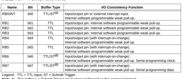
TABLE 4-4: SUMMARY OF REGISTERS ASSOCIATED WITH PORTB
Name Bit Buffer Type I/O Consistency Function
RB0/INT bit0 TTL/ST(1) Input/output pin or external interrupt input. Internal software programmable weak pull-up.
RB1 bit1 TTL Input/output pin. Internal software programmable weak pull-up. RB2 bit2 TTL Input/output pin. Internal software programmable weak pull-up. RB3 bit3 TTL Input/output pin. Internal software programmable weak pull-up.
RB4 bit4 TTL Input/output pin (with interrupt-on-change).
Internal software programmable weak pull-up.
RB5 bit5 TTL Input/output pin (with interrupt-on-change).
Internal software programmable weak pull-up. RB6 bit6 TTL/ST(2) Input/output pin (with interrupt-on-change).
Internal software programmable weak pull-up. Serial programming clock. RB7 bit7 TTL/ST(2) Input/output pin (with interrupt-on-change).
Internal software programmable weak pull-up. Serial programming data. Legend: TTL = TTL input, ST = Schmitt Trigger.
Note 1: This buffer is a Schmitt Trigger input when configured as the external interrupt. 2: This buffer is a Schmitt Trigger input when used in Serial Programming mode.
Address Name Bit 7 Bit 6 Bit 5 Bit 4 Bit 3 Bit 2 Bit 1 Bit 0
Value on Power-on
Reset
Value on all other RESETS
06h PORTB RB7 RB6 RB5 RB4 RB3 RB2 RB1 RB0/INT xxxx xxxx uuuu uuuu
86h TRISB TRISB7 TRISB6 TRISB5 TRISB4 TRISB3 TRISB2 TRISB1 TRISB0 1111 1111 1111 1111
81h OPTION_REG RBPU INTEDG T0CS T0SE PSA PS2 PS1 PS0 1111 1111 1111 1111
0Bh,8Bh INTCON GIE EEIE T0IE INTE RBIE T0IF INTF RBIF 0000 000x 0000 000u
5.0
TIMER0 MODULE
The Timer0 module timer/counter has the following features:
• 8-bit timer/counter • Readable and writable
• Internal or external clock select • Edge select for external clock
• 8-bit software programmable prescaler • Interrupt-on-overflow from FFh to 00h
Figure 5-1 is a simplified block diagram of the Timer0 module.
Additional information on timer modules is available in the PICmicro™ Mid-Range Reference Manual (DS33023).
5.1
Timer0 Operation
Timer0 can operate as a timer or as a counter. Timer mode is selected by clearing bit T0CS (OPTION_REG<5>). In Timer mode, the Timer0 mod-ule will increment every instruction cycle (without pres-caler). If the TMR0 register is written, the increment is inhibited for the following two instruction cycles. The user can work around this by writing an adjusted value to the TMR0 register.
Counter mode is selected by setting bit T0CS (OPTION_REG<5>). In Counter mode, Timer0 will increment, either on every rising or falling edge of pin RA4/T0CKI. The incrementing edge is determined by the Timer0 Source Edge Select bit, T0SE (OPTION_REG<4>). Clearing bit T0SE selects the ris-ing edge. Restrictions on the external clock input are discussed below.
When an external clock input is used for Timer0, it must meet certain requirements. The requirements ensure the external clock can be synchronized with the internal phase clock (TOSC). Also, there is a delay in the actual incrementing of Timer0 after synchronization.
Additional information on external clock requirements is available in the PICmicro™ Mid-Range Reference Manual, (DS33023).
5.2
Prescaler
An 8-bit counter is available as a prescaler for the Timer0 module, or as a postscaler for the Watchdog Timer, respectively (Figure 5-2). For simplicity, this counter is being referred to as “prescaler” throughout this data sheet. Note that there is only one prescaler available which is mutually exclusively shared between the Timer0 module and the Watchdog Timer. Thus, a prescaler assignment for the Timer0 module means that there is no prescaler for the Watchdog Timer, and vice-versa. The prescaler is not readable or writable.
The PSA and PS2:PS0 bits (OPTION_REG<3:0>) determine the prescaler assignment and prescale ratio. Clearing bit PSA will assign the prescaler to the Timer0 module. When the prescaler is assigned to the Timer0 module, prescale values of 1:2, 1:4, ..., 1:256 are selectable.
Setting bit PSA will assign the prescaler to the Watchdog Timer (WDT). When the prescaler is assigned to the WDT, prescale values of 1:1, 1:2, ..., 1:128 are selectable. When assigned to the Timer0 module, all instructions writing to the TMR0 register (e.g., CLRF 1, MOVWF 1,
BSF 1,etc.) will clear the prescaler. When assigned to
WDT, a CLRWDT instruction will clear the prescaler along with the WDT.
FIGURE 5-1: TIMER0 BLOCK DIAGRAM
Note: Writing to TMR0 when the prescaler is
assigned to Timer0 will clear the prescaler count, but will not change the prescaler assignment.
RA4/T0CKI T0SE
0
1
1
0 pin
FOSC/4
Programmable Prescaler
Sync with Internal
Clocks
TMR0 PSOUT
(2 Cycle Delay) PSOUT
Data Bus 8
PSA
PS2, PS1, PS0 Set Interrupt
5.2.1 SWITCHING PRESCALER ASSIGNMENT
The prescaler assignment is fully under software con-trol (i.e., it can be changed “on the fly” during program execution).
5.3
Timer0 Interrupt
The TMR0 interrupt is generated when the TMR0 reg-ister overflows from FFh to 00h. This overflow sets bit T0IF (INTCON<2>). The interrupt can be masked by clearing bit T0IE (INTCON<5>). Bit T0IF must be cleared in software by the Timer0 module Interrupt Ser-vice Routine before re-enabling this interrupt. The TMR0 interrupt cannot awaken the processor from SLEEP since the timer is shut-off during SLEEP.
FIGURE 5-2: BLOCK DIAGRAM OF THE TIMER0/WDT PRESCALER
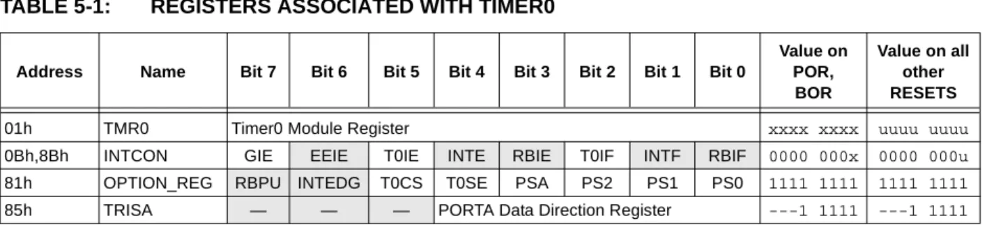
TABLE 5-1: REGISTERS ASSOCIATED WITH TIMER0
Note: To avoid an unintended device RESET, a specific instruction sequence (shown in the PICmicro™ Mid-Range Reference Man-ual, DS33023) must be executed when changing the prescaler assignment from Timer0 to the WDT. This sequence must be followed even if the WDT is disabled.
RA4/T0CKI
T0SE pin
M U X CLKOUT (= FOSC/4)
SYNC 2 Cycles
TMR0 reg
8-bit Prescaler
8 - to - 1 MUX M
U X
M U X Watchdog
Timer
PSA
0 1
0
1
WDT Time-out
PS2:PS0 8
Note: T0CS, T0SE, PSA, PS2:PS0 are (OPTION_REG<5:0>).
PSA WDT Enable bit
M U X 0
1 0
1
Data Bus
Set Flag bit T0IF on Overflow 8
PSA T0CS
Address Name Bit 7 Bit 6 Bit 5 Bit 4 Bit 3 Bit 2 Bit 1 Bit 0
Value on POR,
BOR
Value on all other RESETS
01h TMR0 Timer0 Module Register xxxx xxxx uuuu uuuu
0Bh,8Bh INTCON GIE EEIE T0IE INTE RBIE T0IF INTF RBIF 0000 000x 0000 000u
81h OPTION_REG RBPU INTEDG T0CS T0SE PSA PS2 PS1 PS0 1111 1111 1111 1111
85h TRISA — — — PORTA Data Direction Register ---1 1111 ---1 1111
6.0
SPECIAL FEATURES OF THE
CPU
What sets a microcontroller apart from other processors are special circuits to deal with the needs of real time applications. The PIC16F84A has a host of such features intended to maximize system reliability, minimize cost through elimination of external components, provide power saving operating modes and offer code protection. These features are:
• OSC Selection • RESET
- Power-on Reset (POR) - Power-up Timer (PWRT) - Oscillator Start-up Timer (OST) • Interrupts
• Watchdog Timer (WDT) • SLEEP
• Code Protection • ID Locations
• In-Circuit Serial Programming™ (ICSP™)
The PIC16F84A has a Watchdog Timer which can be shut-off only through configuration bits. It runs off its own RC oscillator for added reliability. There are two timers that offer necessary delays on power-up. One is the Oscillator Start-up Timer (OST), intended to keep
the chip in RESET until the crystal oscillator is stable. The other is the Power-up Timer (PWRT), which pro-vides a fixed delay of 72 ms (nominal) on power-up only. This design keeps the device in RESET while the power supply stabilizes. With these two timers on-chip, most applications need no external RESET circuitry. SLEEP mode offers a very low current power-down mode. The user can wake-up from SLEEP through external RESET, Watchdog Timer Time-out or through an interrupt. Several oscillator options are provided to allow the part to fit the application. The RC oscillator option saves system cost while the LP crystal option saves power. A set of configuration bits are used to select the various options.
Additional information on special features is available in the PICmicro™ Mid-Range Reference Manual (DS33023).
6.1
Configuration Bits
The configuration bits can be programmed (read as '0'), or left unprogrammed (read as '1'), to select various device configurations. These bits are mapped in program memory location 2007h.
Address 2007h is beyond the user program memory space and it belongs to the special test/configuration memory space (2000h - 3FFFh). This space can only be accessed during programming.
REGISTER 6-1: PIC16F84A CONFIGURATION WORD
R/P-u R/P-u R/P-u R/P-u R/P-u R/P-u R/P-u R/P-u R/P-u R/P-u R/P-u R/P-u R/P-u R/P-u
CP CP CP CP CP CP CP CP CP CP PWRTE WDTE F0SC1 F0SC0
bit13 bit0
bit 13-4 CP: Code Protection bit 1 = Code protection disabled
0 = All program memory is code protected bit 3 PWRTE: Power-up Timer Enable bit
1 = Power-up Timer is disabled
0 = Power-up Timer is enabled bit 2 WDTE: Watchdog Timer Enable bit
1 = WDT enabled
0 = WDT disabled
bit 1-0 FOSC1:FOSC0: Oscillator Selection bits 11 = RC oscillator
10 = HS oscillator
01 = XT oscillator
6.2
Oscillator Configurations
6.2.1 OSCILLATOR TYPES
The PIC16F84A can be operated in four different oscillator modes. The user can program two configuration bits (FOSC1 and FOSC0) to select one of these four modes:
• LP Low Power Crystal • XT Crystal/Resonator
• HS High Speed Crystal/Resonator • RC Resistor/Capacitor
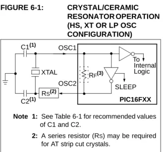
6.2.2 CRYSTAL OSCILLATOR/CERAMIC
RESONATORS
In XT, LP, or HS modes, a crystal or ceramic resonator is connected to the OSC1/CLKIN and OSC2/CLKOUT pins to establish oscillation (Figure 6-1).
FIGURE 6-1: CRYSTAL/CERAMIC
RESONATOR OPERATION (HS, XT OR LP OSC CONFIGURATION)
The PIC16F84A oscillator design requires the use of a parallel cut crystal. Use of a series cut crystal may give a frequency out of the crystal manufacturers specifications. When in XT, LP, or HS modes, the device can have an external clock source to drive the OSC1/CLKIN pin (Figure 6-2).
FIGURE 6-2: EXTERNAL CLOCK INPUT
OPERATION (HS, XT OR LP OSC
CONFIGURATION)
TABLE 6-1: CAPACITOR SELECTION FOR
CERAMIC RESONATORS
Note 1: See Table 6-1 for recommended values of C1 and C2.
2: A series resistor (RS) may be required for AT strip cut crystals.
C1(1)
C2(1) XTAL
OSC2 OSC1
RF(3)
SLEEP To
Logic
PIC16FXX RS(2)
Internal
Ranges Tested:
Mode Freq OSC1/C1 OSC2/C2
XT 455 kHz
2.0 MHz 4.0 MHz
47 - 100 pF 15 - 33 pF 15 - 33 pF
47 - 100 pF 15 - 33 pF 15 - 33 pF
HS 8.0 MHz
10.0 MHz
15 - 33 pF 15 - 33 pF
15 - 33 pF 15 - 33 pF
Note: Recommended values of C1 and C2 are
identical to the ranges tested in this table. Higher capacitance increases the stability of the oscillator, but also increases the start-up time. These values are for design guidance only. Since each resonator has its own characteristics, the user should consult the resonator manufacturer for the appropriate values of external compo-nents.
Note: When using resonators with frequencies above 3.5 MHz, the use of HS mode rather than XT mode, is recommended. HS mode may be used at any VDD for which the controller is rated.
OSC1
OSC2 Open
Clock from
TABLE 6-2: CAPACITOR SELECTION FOR CRYSTAL OSCILLATOR
6.2.3 RC OSCILLATOR
For timing insensitive applications, the RC device option offers additional cost savings. The RC oscillator frequency is a function of the supply voltage, the resistor (REXT) values, capacitor (CEXT) values, and the operating temperature. In addition to this, the oscil-lator frequency will vary from unit to unit due to normal process parameter variation. Furthermore, the difference in lead frame capacitance between package types also affects the oscillation frequency, especially for low CEXT values. The user needs to take into account variation, due to tolerance of the external R and C components. Figure 6-3 shows how an R/C combination is connected to the PIC16F84A.
FIGURE 6-3: RC OSCILLATOR MODE
Mode Freq OSC1/C1 OSC2/C2
LP 32 kHz
200 kHz
68 - 100 pF 15 - 33 pF
68 - 100 pF 15 - 33 pF
XT 100 kHz
2 MHz 4 MHz
100 - 150 pF 15 - 33 pF 15 - 33 pF
100 - 150 pF 15 - 33 pF 15 - 33 pF
HS 4 MHz
20 MHz
15 - 33 pF 15 - 33 pF
15 - 33 pF 15 - 33 pF Note: Higher capacitance increases the stability
of the oscillator, but also increases the start-up time. These values are for design guidance only. Rs may be required in HS mode, as well as XT mode, to avoid over-driving crystals with low drive level specifi-cation. Since each crystal has its own characteristics, the user should consult the crystal manufacturer for appropriate values of external components.
For VDD > 4.5V, C1 = C2 ≈ 30 pF is recom-mended.
OSC2/CLKOUT CEXT
REXT
PIC16FXX OSC1
FOSC/4
Internal Clock VDD
VSS
Recommended values: 5 kΩ≤ REXT ≤ 100 kΩ CEXT > 20pF
6.3
RESET
The PIC16F84A differentiates between various kinds of RESET:
• Power-on Reset (POR) • MCLR during normal operation • MCLR during SLEEP
• WDT Reset (during normal operation) • WDT Wake-up (during SLEEP)
Figure 6-4 shows a simplified block diagram of the On-Chip RESET Circuit. The MCLR Reset path has a noise filter to ignore small pulses. The electrical speci-fications state the pulse width requirements for the MCLR pin.
Some registers are not affected in any RESET condition; their status is unknown on a POR and unchanged in any other RESET. Most other registers are reset to a “RESET state” on POR, MCLR or WDT Reset during normal oper-ation and on MCLR during SLEEP. They are not affected by a WDT Reset during SLEEP, since this RESET is viewed as the resumption of normal operation.
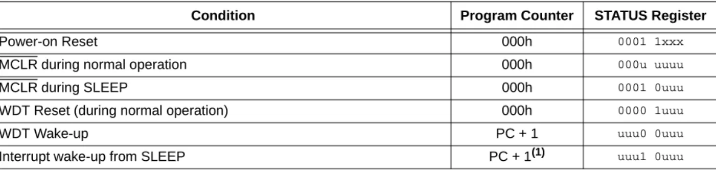
Table 6-3 gives a description of RESET conditions for the program counter (PC) and the STATUS register. Table 6-4 gives a full description of RESET states for all registers.
The TO and PD bits are set or cleared differently in dif-ferent RESET situations (Section 6.7). These bits are used in software to determine the nature of the RESET.
FIGURE 6-4: SIMPLIFIED BLOCK DIAGRAM OF ON-CHIP RESET CIRCUIT
TABLE 6-3: RESET CONDITION FOR PROGRAM COUNTER AND THE STATUS REGISTER
S
R Q
External Reset MCLR
VDD
OSC1/
WDT Module VDD Rise
Detect OST/PWRT
On-Chip RC Osc(1)
WDT Time-out
Power-on Reset
OST
10-bit Ripple Counter
PWRT
Chip_Reset
10-bit Ripple Counter Reset
Enable OST Enable PWRT SLEEP
CLKIN
Note 1: This is a separate oscillator from the RC oscillator of the CLKIN pin. 2: See Table 6-5.
See Table 6-5
Condition Program Counter STATUS Register
Power-on Reset 000h 0001 1xxx
MCLR during normal operation 000h 000u uuuu
MCLR during SLEEP 000h 0001 0uuu
WDT Reset (during normal operation) 000h 0000 1uuu
WDT Wake-up PC + 1 uuu0 0uuu
Interrupt wake-up from SLEEP PC + 1(1) uuu1 0uuu
Legend:u = unchanged, x = unknown
TABLE 6-4: RESET CONDITIONS FOR ALL REGISTERS
Register Address Power-on Reset
MCLR during: – normal operation – SLEEP
WDT Reset during normal operation
Wake-up from SLEEP: – through interrupt – through WDT Time-out
W — xxxx xxxx uuuu uuuu uuuu uuuu
INDF 00h ---- ---- ---- ----
----TMR0 01h xxxx xxxx uuuu uuuu uuuu uuuu
PCL 02h 0000 0000 0000 0000 PC + 1(2)
STATUS 03h 0001 1xxx 000q quuu(3) uuuq quuu(3)
FSR 04h xxxx xxxx uuuu uuuu uuuu uuuu
PORTA(4) 05h ---x xxxx ---u uuuu ---u uuuu
PORTB(5) 06h xxxx xxxx uuuu uuuu uuuu uuuu
EEDATA 08h xxxx xxxx uuuu uuuu uuuu uuuu
EEADR 09h xxxx xxxx uuuu uuuu uuuu uuuu
PCLATH 0Ah ---0 0000 ---0 0000 ---u uuuu
INTCON 0Bh 0000 000x 0000 000u uuuu uuuu(1)
INDF 80h ---- ---- ---- ----
----OPTION_REG 81h 1111 1111 1111 1111 uuuu uuuu
PCL 82h 0000 0000 0000 0000 PC + 1(2)
STATUS 83h 0001 1xxx 000q quuu(3) uuuq quuu(3)
FSR 84h xxxx xxxx uuuu uuuu uuuu uuuu
TRISA 85h ---1 1111 ---1 1111 ---u uuuu
TRISB 86h 1111 1111 1111 1111 uuuu uuuu
EECON1 88h ---0 x000 ---0 q000 ---0 uuuu
EECON2 89h ---- ---- ---- ----
----PCLATH 8Ah ---0 0000 ---0 0000 ---u uuuu
INTCON 8Bh 0000 000x 0000 000u uuuu uuuu(1)
Legend:u = unchanged, x = unknown, - = unimplemented bit, read as '0', q = value depends on condition Note 1: One or more bits in INTCON will be affected (to cause wake-up).
2: When the wake-up is due to an interrupt and the GIE bit is set, the PC is loaded with the interrupt vector (0004h).
3: Table 6-3 lists the RESET value for each specific condition. 4: On any device RESET, these pins are configured as inputs. 5: This is the value that will be in the port output latch.
6.4
Power-on Reset (POR)
A Power-on Reset pulse is generated on-chip when VDD rise is detected (in the range of 1.2V - 1.7V). To take advantage of the POR, just tie the MCLR pin directly (or through a resistor) to VDD. This will eliminate external RC components usually needed to create Power-on Reset. A minimum rise time for VDD must be met for this to operate properly. See Electrical Specifications for details.
When the device starts normal operation (exits the RESET condition), device operating parameters (volt-age, frequency, temperature, etc.) must be met to ensure operation. If these conditions are not met, the device must be held in RESET until the operating con-ditions are met.
For additional information, refer to Application Note AN607, "Power-up Trouble Shooting."
The POR circuit does not produce an internal RESET when VDD declines.
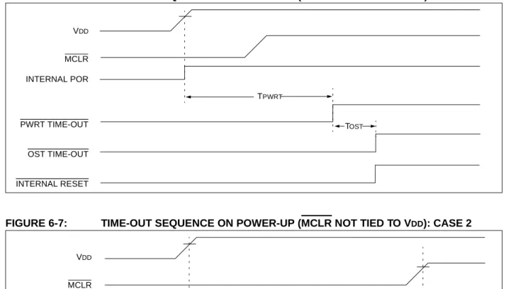
6.5
Power-up Timer (PWRT)
The Power-up Timer (PWRT) provides a fixed 72 ms nominal time-out (TPWRT) from POR (Figures 6-6 through 6-9). The Power-up Timer operates on an internal RC oscillator. The chip is kept in RESET as long as the PWRT is active. The PWRT delay allows the VDD to rise to an acceptable level (possible excep-tion shown in Figure 6-9).
A configuration bit, PWRTE, can enable/disable the PWRT. See Register 6-1 for the operation of the PWRTE bit for a particular device.
The power-up time delay TPWRT will vary from chip to chip due to VDD, temperature, and process variation. See DC parameters for details.
6.6
Oscillator Start-up Timer (OST)
The Oscillator Start-up Timer (OST) provides a 1024 oscillator cycle delay (from OSC1 input) after the PWRT delay ends (Figure 6-6, Figure 6-7, Figure 6-8 and Figure 6-9). This ensures the crystal oscillator or resonator has started and stabilized.
The OST time-out (TOST) is invoked only for XT, LP and HS modes and only on Power-on Reset or wake-up from SLEEP.
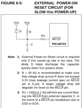
When VDD rises very slowly, it is possible that the TPWRT time-out and TOST time-out will expire before VDD has reached its final value. In this case (Figure 6-9), an external Power-on Reset circuit may be necessary (Figure 6-5).
FIGURE 6-5: EXTERNAL POWER-ON
RESET CIRCUIT (FOR
SLOW VDD POWER-UP)
Note 1: External Power-on Reset circuit is required only if VDD power-up rate is too slow. The diode D helps discharge the capacitor quickly when VDD powers down.
2: R < 40 kΩ is recommended to make sure that voltage drop across R does not exceed 0.2V (max leakage current spec on MCLR pin is 5µA). A larger voltage drop will degrade VIH level on the MCLR pin. 3: R1 = 100Ω to 1 kΩ will limit any current
flow-ing into MCLR from external capacitor C, in the event of a MCLR pin breakdown due to ESD or EOS.
C R1 R
D VDD
MCLR PIC16FXX VDD
FIGURE 6-6: TIME-OUT SEQUENCE ON POWER-UP (MCLR NOT TIED TO VDD): CASE 1
FIGURE 6-7: TIME-OUT SEQUENCE ON POWER-UP (MCLR NOT TIED TO VDD): CASE 2
FIGURE 6-8: TIME-OUT SEQUENCE ON POWER-UP (MCLR TIED TO VDD): FAST VDD RISE
TIME
TPWRT
TOST VDD
MCLR INTERNAL POR
PWRT TIME-OUT
OST TIME-OUT
INTERNAL RESET
VDD
MCLR INTERNAL POR
PWRT TIME-OUT
OST TIME-OUT
INTERNAL RESET
TPWRT
TOST
VDD
MCLR INTERNAL POR
TPWRT
TOST PWRT TIME-OUT
FIGURE 6-9: TIME-OUT SEQUENCE ON POWER-UP (MCLR TIED TO VDD):
SLOW VDD RISE TIME
6.7
Time-out Sequence and
Power-down Status Bits (TO/PD)
On power-up (Figures 6-6 through 6-9), the time-out sequence is as follows:
1. PWRT time-out is invoked after a POR has expired.
2. Then, the OST is activated.
The total time-out will vary based on oscillator configu-ration and PWRTE configuconfigu-ration bit status. For exam-ple, in RC mode with the PWRT disabled, there will be no time-out at all.
TABLE 6-5: TIME-OUT IN VARIOUS
SITUATIONS
Since the time-outs occur from the POR pulse, if MCLR is kept low long enough, the time-outs will expire. Then bringing MCLR high, execution will begin immediately (Figure 6-6). This is useful for testing purposes or to synchronize more than one PIC16F84A device when operating in parallel.
Table 6-6 shows the significance of the TO and PD bits. Table 6-3 lists the RESET conditions for some special registers, while Table 6-4 lists the RESET conditions for all the registers.
TABLE 6-6: STATUS BITS AND THEIR
SIGNIFICANCE VDD
MCLR
V1
When VDD rises very slowly, it is possible that the TPWRT time-out and TOST time-out will expire before VDD has reached its final value. In this example, the chip will reset properly if, and only if, V1 ≥ VDD min. INTERNAL POR
TPWRT
TOST PWRT TIME-OUT
OST TIME-OUT
INTERNAL RESET
Oscillator Configuration
Power-up Wake-up
from SLEEP PWRT
Enabled
PWRT Disabled XT, HS, LP 72 ms +
1024TOSC 1024TOSC 1024TOSC
RC 72 ms — —
TO PD Condition
1 1 Power-on Reset
0 x Illegal, TO is set on POR x 0 Illegal, PD is set on POR
0 1 WDT Reset (during normal operation)
0 0 WDT Wake-up
1 1 MCLR during normal operation 1 0 MCLR during SLEEP or interrupt
6.8
Interrupts
The PIC16F84A has 4 sources of interrupt: • External interrupt RB0/INT pin
• TMR0 overflow interrupt
• PORTB change interrupts (pins RB7:RB4) • Data EEPROM write complete interrupt
The interrupt control register (INTCON) records individual interrupt requests in flag bits. It also contains the individual and global interrupt enable bits. The global interrupt enable bit, GIE (INTCON<7>), enables (if set) all unmasked interrupts or disables (if cleared) all interrupts. Individual interrupts can be disabled through their corresponding enable bits in INTCON register. Bit GIE is cleared on RESET. The “return from interrupt” instruction, RETFIE, exits interrupt routine as well as sets the GIE bit, which re-enables interrupts.
The RB0/INT pin interrupt, the RB port change interrupt and the TMR0 overflow interrupt flags are contained in the INTCON register.
When an interrupt is responded to, the GIE bit is cleared to disable any further interrupt, the return address is pushed onto the stack and the PC is loaded with 0004h. For external interrupt events, such as the RB0/INT pin or PORTB change interrupt, the interrupt latency will be three to four instruction cycles. The exact latency depends when the interrupt event occurs. The latency is the same for both one and two cycle instructions. Once in the Interrupt Service Routine, the source(s) of the interrupt can be determined by polling the interrupt flag bits. The interrupt flag bit(s) must be cleared in software before re-enabling interrupts to avoid infinite interrupt requests.
FIGURE 6-10: INTERRUPT LOGIC
6.8.1 INT INTERRUPT
External interrupt on RB0/INT pin is edge triggered: either rising if INTEDG bit (OPTION_REG<6>) is set, or falling if INTEDG bit is clear. When a valid edge appears on the RB0/INT pin, the INTF bit (INTCON<1>) is set. This interrupt can be disabled by clearing control bit INTE (INTCON<4>). Flag bit INTF must be cleared in software via the Interrupt Service Routine before re-enabling this interrupt. The INT interrupt can wake the processor from SLEEP (Section 6.11) only if the INTE bit was set prior to going into SLEEP. The status of the GIE bit decides whether the processor branches to the interrupt vector following wake-up.
6.8.2 TMR0 INTERRUPT
An overflow (FFh → 00h) in TMR0 will set flag bit T0IF (INTCON<2>). The interrupt can be enabled/disabled by setting/clearing enable bit T0IE (INTCON<5>) (Section 5.0).
6.8.3 PORTB INTERRUPT
An input change on PORTB<7:4> sets flag bit RBIF (INTCON<0>). The interrupt can be enabled/disabled by setting/clearing enable bit RBIE (INTCON<3>) (Section 4.2).
6.8.4 DATA EEPROM INTERRUPT
At the completion of a data EEPROM write cycle, flag bit EEIF (EECON1<4>) will be set. The interrupt can be enabled/disabled by setting/clearing enable bit EEIE (INTCON<6>) (Section 3.0).
Note: Individual interrupt flag bits are set regardless of the status of their corresponding mask bit or the GIE bit.
RBIF RBIE T0IF T0IE INTF INTE
GIE EEIE
Wake-up (If in SLEEP mode)
Interrupt to CPU
EEIF
Note: For a change on the I/O pin to be
recognized, the pulse width must be at least TCY wide.
6.9
Context Saving During Interrupts
During an interrupt, only the return PC value is saved on the stack. Typically, users wish to save key register values during an interrupt (e.g., W register and STATUS register). This is implemented in software. The code in Example 6-1 stores and restores the STATUS and W register’s values. The user defined registers, W_TEMP and STATUS_TEMP are the tem-porary storage locations for the W and STATUS registers values.
Example 6-1 does the following: a) Stores the W register.
b) Stores the STATUS register in STATUS_TEMP. c) Executes the Interrupt Service Routine code. d) Restores the STATUS (and bank select bit)
register.
e) Restores the W register.
EXAMPLE 6-1: SAVING STATUS AND W REGISTERS IN RAM
6.10
Watchdog Timer (WDT)
The Watchdog Timer is a free running On-Chip RC Oscillator which does not require any external components. This RC oscillator is separate from the RC oscillator of the OSC1/CLKIN pin. That means that the WDT will run even if the clock on the OSC1/CLKIN and OSC2/CLKOUT pins of the device has been stopped, for example, by execution of a SLEEP
instruction. During normal operation, a WDT time-out generates a device RESET. If the device is in SLEEP mode, a WDT wake-up causes the device to wake-up and continue with normal operation. The WDT can be permanently disabled by programming configuration bit WDTE as a '0' (Section 6.1).
6.10.1 WDT PERIOD
The WDT has a nominal time-out period of 18 ms, (with no prescaler). The time-out periods vary with temperature, VDD and process variations from part to part (see DC specs). If longer time-out periods are desired, a prescaler with a division ratio of up to 1:128 can be assigned to the WDT under software control by writing to the OPTION_REG register. Thus, time-out periods up to 2.3 seconds can be realized.
The CLRWDT and SLEEP instructions clear the WDT
and the postscaler (if assigned to the WDT) and pre-vent it from timing out and generating a device RESET condition.
The TO bit in the STATUS register will be cleared upon a WDT time-out.
PUSH MOVWF W_TEMP ; Copy W to TEMP register,
SWAPF STATUS, W ; Swap status to be saved into W MOVWF STATUS_TEMP ; Save status to STATUS_TEMP register
ISR : :
: ; Interrupt Service Routine
: ; should configure Bank as required
: ;
POP SWAPF STATUS_TEMP,W ; Swap nibbles in STATUS_TEMP register ; and place result into W
MOVWF STATUS ; Move W into STATUS register
; (sets bank to original state)
SWAPF W_TEMP, F ; Swap nibbles in W_TEMP and place result in W_TEMP SWAPF W_TEMP, W ; Swap nibbles in W_TEMP and place result into W