An Energy-aware Dynamic Data Allocation Mechanism
for Many-channel Memory Systems
Masayuki Sato1 , Takuya Toyoshima1, Hikaru Takayashiki1 , Ryusuke Egawa1 , Hiroaki Kobayashi1
c
The Authors 2019. This paper is published with open access at SuperFri.org
A modern memory system is equipped with many memory channels to obtain a high memory bandwidth. To take the advantage of this organization, applications’ data are distributed among the channels and transferred in an interleaved fashion. Although memory-intensive applications benefit from a high bandwidth by many memory channels, applications such as compute-intensive ones do not need the high bandwidth. To reduce the energy consumption for such applications, the memory system haslow-power modes. During no memory request, the main memory can enter these modes and reduce energy consumption. However, these applications often cause intermittent memory requests to the channels that handle their data, resulting in not entering the low-power modes. Hence, the memory system cannot enter the low-power modes even though the applications do not need the high bandwidth. To solve this problem, this paper proposes a dynamic data allocation mechanism for many-channel memory systems. This mechanism forces data of such applications to use the specified channels by dynamically changing the address-mapping schemes and migrating the data. As a result, the other channels to which the data are not allocated can have a chance to enter the low-power modes for a long time. Therefore, the proposed mechanism has the potential to reduce the energy consumption of many-channel memory systems. The evaluation results show that this mechanism can reduce the energy consumption by up to 11.8% and 1.7% on average.
Keywords: DRAM, main memory, low-power mode, address-mapping scheme, energy con-sumption.
Introduction
Modern microprocessors have improved their performances by increasing the numbers of cores significantly [3]. As a result, a high memory bandwidth is required by a microprocessor and applications executed on it [16]. On the other hand, the speed of Dynamic Random Access Memory (DRAM), which is used as a main memory, has modestly improved. Due to the perfor-mance gap between microprocessors and main memories, the main memories cannot supply the data at enough speed to the microprocessor. Therefore, a main memory has been a bottleneck in the performance of a modern computing system. This problem is well-known as the “Memory Wall” problem [18].
To cope with such a situation, the latest computing systems have a main memory system
with many memory channels to obtain the higher memory bandwidth. Such a many-channel
memory system is widely employed in industrial microprocessors from personal computers to supercomputer systems. For example, a memory module with 3D-integration technologies, High Bandwidth Memory (HBM), has 8 channels physically, and can act as a 16-channel module in the pseudo-channel mode [13]. Since six HBM modules can be integrated with a microprocessor on a silicon interposer [19], it is possible for a single memory system to have 48 to 96 channels. On the other hand, not all applications require such a high memory bandwidth. As the diver-sity among applications increases, the applications could be categorized into memory-intensive and compute-intensive applications. The compute-intensive applications do not always need high bandwidths. For these applications, such a high bandwidth memory has a little performance
im-1Tohoku University, Sendai, Japan
pact and causes a high energy consumption. To reduce the energy consumption of the memory system in compute-intensive applications, DRAM-based memory systems have several low-power modes. These modes can reduce the power consumption by deactivating peripheral circuits of DRAM chips when the compute-intensive applications do not need the memory performance.
However, to take the advantages of using many channels simultaneously and get their full bandwidth, the data of an application are distributed among all the memory channels in an
interleaved fashion, determined byan address-mapping scheme. Since the data placement for any
applications is treated under a single address-mapping scheme, the data of the compute-intensive applications are also distributed. If these applications intermittently cause memory requests to all the channels, memory systems cannot enter the low-power modes, although they do not need to use the whole bandwidth. Therefore, address-mapping schemes should be appropriately selected so that the memory system can reduce the energy consumption by aggressively using the low-power modes.
To solve this problem, this paper proposes an energy-aware dynamic data allocation mech-anism for many-channel memory systems. This mechmech-anism dynamically switches two address-mapping schemes based on the access frequencies. One scheme is to distribute the data among channels, and the other scheme is to gather the data into specific memory channels. When the applications do not need to use all of the channels for the highest bandwidth, this mechanism selects the scheme that gathers the data accessed frequently into limited memory channels. By selecting this scheme, the access frequencies to the other channels can be reduced, and these channels can get more opportunities to enter the low-power modes. Therefore, this mechanism has the potential to reduce the energy consumption of many-channel memory systems. Note that, if the proposed mechanism switches the address-mapping schemes without caring the data, a memory system cannot correctly provide the data that are stored based on the address-mapping scheme used before the switching. To avoid such a situation, the proposed mechanism migrates data stored by the previous scheme so that they can be accessed by the current scheme. There-fore, the proposed mechanism can continue to correctly process the memory requests.
The rest of this paper is organized as follows. Section 1 explains the low-power modes and discusses the effectiveness of the low-power modes. Section 2 discusses address-mapping schemes to change the number of accessed channels, and proposes a dynamic mechanism that changes these schemes during an execution to reflect the demand for the memory bandwidth of applications. Section 3 shows the evaluation results that support the effectiveness of the proposed mechanism. The final section concludes this paper.
1. Power Management of Memory Systems
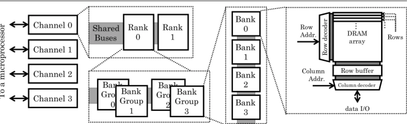
1.1. Basic Organization of a DRAM-based Memory System
Bank 0 Bank
1 Bank
2 Bank
3 Channel 0
Channel 1
Channel 2
Channel 3
T
o
a
m
ic
rop
roc
es
sor Shared Rank0 Rank1
Buses DRAMarray
Row buffer
R
ow
d
ec
od
er
Column decoder Row
Addr.
Column Addr.
data I/O
Rows
… …
Bank Group
0
Bank Group
2 Bank Group
1
Bank Group
3
Figure 1.Overview of a memory system
accompanied by peripheral circuits to read/write data from/to a single row, and provide data in columns to the microprocessor.
The procedure to access the data is summarized in the following three steps. All the
com-mands for these steps pass through the shared buses. The first step isprecharge. This step sets
up banks that include the accessed data. In this step, a row buffer adjoining each bank is cleared with writing its data back to the DRAM cells, and the banks and their peripheral circuits are
prepared for the next step. The next step is row activation. In this step, one of the rows in the
bank is specified by the row decoder, and then the data in the row are read out to the row buffer.
The third step is column read/write. In this step, the column in the row buffer is specified. In
the case of a read request, the column data are read out from the row buffer to the shared data bus. In the case of a write request, the data sent from the shared bus are stored in the target column in the row buffer.
To access the data based on these steps, it is requested to determine which bank, row, column, and rank should be accessed. To this end, the physical address included in a memory request is used. From the bit sequence of the physical address, the IDs of these hierarchical components are extracted as subsets of the bit sequence. A rule that determines how these IDs
are taken from the physical address is called an address-mapping scheme.
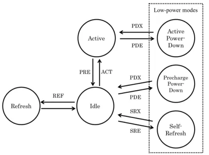
1.2. Low-power Mode
Figure 2 shows the state transition diagram of a DRAM chip. Each state corresponds to each mode that the DRAM chip can transit. Idle mode is an initial state. If a bank receives the
row-activation command (ACT), the bank transits to the state active. In this state, the bank
can accept read/write operations issued by the column read and write commands. On the other hand, when the bank receives the precharge command (PRE), the state of the bank returns to idle. In the case where all the banks in the rank become the Idle state and receive the refresh command (REF), the rank starts to refresh data to avoid the DRAM cells from losing the data by leakage current.
For reducing the energy consumption of DRAM-based memory systems, the DRAM stan-dards include the low-power modes. A rank can enter the low-power mode under the conditions that there is no waiting command based on the memory request to the banks, and the rank
receives command PDX or SRX. As shown in Fig. 2, there are several low-power modes, e.g.,
Precharge
Power-Down
Idle Active
Refresh
Active Power-Down
Self-Refresh
ACT PRE
PDE PDX
REF PDE
PDX
SRE SRX
Low-power modes
Figure 2.State transition diagram of power modes
1.3. Limitation of the Deep Low-power Mode
To reduce the power consumption of the memory system, the low-power mode should be appropriately used. This is because the energy consumption may increase due to the latency for the recovery from the low-power modes to the active mode. To obtain the target data in the rank in the low-power modes, the memory requests have to wait for the recovery of the ranks from the low-power modes. The recovery process needs to enable the power supply for the disabled circuits, resulting in a certain latency. If accesses invoke the recovery process frequently, the accumulated latency may cause a significant performance penalty for the executed application. As a result, the execution time of the application and the energy consumption may increase even if the power consumption decreases. Among the three low-power modes, the self-refresh mode is the most effective to reduce the power consumption, but the recovery latency is also the largest among them, which results in the large performance penalty [14].
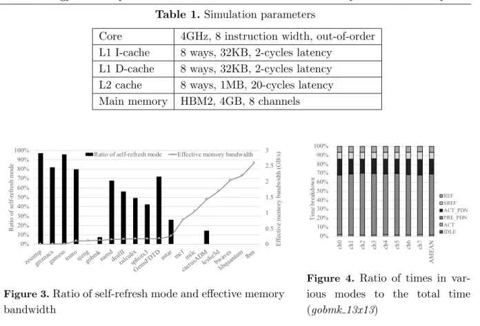
To evaluate how the low-power modes, especially the self-refresh mode, can be exploited in a modern memory system, the preliminary evaluation is conducted by simulation. The target system has a 4GB HBM2 memory module for the main memory. The detailed parameters of the system are shown in Tab. 1. The latency parameters of HBM2 refer to [4], and the cur-rent parameters are based on those of a DDR4 module that has the same voltage and clock frequency [11]. In this simulation, the gem5 simulator system [1] is used. Applications executed on the simulator are selected from the SPEC CPU2006 benchmark suite. Each application is executed by three billion instructions after skipping the first one billion instructions.
The details of the self-refresh mode are as follows. Generally, to suppress the performance penalty, the rank can enter the self-refresh mode after a certain idle period has continued. In ad-dition, one normal refresh operation should be done before moving to the self-refresh mode [11]. Therefore, in this simulation experiment, the rank enters the self-refresh mode after the condi-tions that a certain period without access is elapsed, and one refresh operation completes. The period is empirically determined as 78,000 cycles so that the performance degradation due to the self-refresh mode becomes less than 1%.
Table 1. Simulation parameters
Core 4GHz, 8 instruction width, out-of-order
L1 I-cache 8 ways, 32KB, 2-cycles latency
L1 D-cache 8 ways, 32KB, 2-cycles latency
L2 cache 8 ways, 1MB, 20-cycles latency
Main memory HBM2, 4GB, 8 channels
0 0.5 1 1.5 2 2.5 3 0% 10% 20% 30% 40% 50% 60% 70% 80% 90% 100%
zeusmpgrom acs
game ss
tontosjenggobmknamddealI I calcul ix sphinx3 Gems FDT
Dastar mcf milc
cactus ADMleslie3d
bwave s libqua ntum lbm E ff ec ti ve m em or y ba ndw idt h ( G B /s ) R at io of s el f-re fr es h m ode
Ratio of self-refresh mode Effective memory bandwidth
Figure 3.Ratio of self-refresh mode and effective memory
bandwidth 0% 10% 20% 30% 40% 50% 60% 70% 80% 90% 100%
ch0 ch1 ch2 ch3 ch4 ch5 ch6 ch7
AM E AN Ti m e br ea kdow n REF SREF ACT_PDN PRE_PDN ACT IDLE
Figure 4. Ratio of times in
var-ious modes to the total time (gobmk 13x13)
The right vertical axis and the line graph indicate the effective memory bandwidth in the case without the self-refresh mode. All of these values are averaged by those of all the eight channels. Figure 3 shows the trend that the ratio of the self-refresh mode becomes smaller as the sustained memory bandwidth increases. This trend is very intuitive. As the number of memory requests increases, the idle time between a request and its subsequent one becomes shorter. Hence, the memory system cannot easily enter the self-refresh mode.
Focusing on each benchmark, the ratios of the self-refresh mode in some benchmarks are
very low, 0.08% in sjengand 7.8% ingobmk, respectively. Each of the benchmarks cannot enter
the self-refresh mode at all while its effective bandwidth is low enough compared with the other applications. To more deeply discuss this fact, Fig. 4 shows the breakdown of the total execution
time into times for individual modes in gobmk. This graph shows the results of all the channels.
Figure 4 shows that the ratio of the self-refresh mode (SREF) to the total time is only 8%.
In contrast, the precharge power-down mode (PRE PDN) is dominant. This fact means that
the time duration between one request and the subsequent request is long enough to enter the precharge power-down mode but too short to enter the self-refresh mode. This situation occurs for all the channels. Therefore, these results indicate that it is difficult to fully exploit the self-refresh mode for the applications that cause memory requests intermittently.
1.4. Related Work
This section reviews the related work to reduce the power and energy consumption of the DRAM-based memory systems.
While this paper focuses on power management using channels, there are some studies
focus-ing on power management usfocus-ing memory ranks. Lebecket al.[9] have discussed how to effectively
use DRAM chips including the low-power modes. They have investigated the parameters to en-ter the low-power modes, and show the first preliminary results of the frequency-based page
allocation, which determines the page allocation based on the access frequency. Wu et al.have
proposed RAMZzz [17]. Because applications generally have different access locality, RAMZzz
dynamically migrates the memory pages, which are accessed frequently, into some of the ranks. Since the other ranks store only the pages that are less accessed, these ranks can obtain more
room to enter the low-power mode. Jang et al. [8] have proposed a rank-aware power
manage-ment method considering the virtual machines to reduce the memory power consumption of data centers. This work considers the scheduling of virtual machines and the placement of their data on the memory system together. The data of virtual machines that are simultaneously executed
in multiple cores are gathered into the same memory ranks. Sato et al. [12] have proposed a
rank-based power management method using multiple address-mapping schemes. Each of the address-mapping schemes determines how data with a physical address is mapped to a physical position of a DRAM-based memory system. By changing the address-mapping schemes, the proposal can gather the data into a single rank or distribute the data across multiple ranks regardless of applications and virtual machines. However, the address-mapping schemes have the limitations, and this method cannot exploit all the ranks to increase the performance.
One of the potential problems of these four studies mentioned above is that the power/energy management is done by controlling ranks. These proposals can work on a memory system with multiple ranks and becomes effective as the number of ranks increases. On the other hand, there are systems that have only one rank in reality. For example, there are typical cases that a personal computer has two DIMM modules, each of which has one rank. However, these modules are generally used for increasing the number of channels for performance improvement, not for increasing the number of ranks per channel. Moreover, the latest high-performance memory module, HBM2, has 8 channels but only one rank [13]. In such cases, the rank-based power management methods cannot be applied.
Huret al. have proposed theadaptive memory throttling[6]. This method purposely blocks the incoming memory commands during a certain period. By delaying the commands, the mem-ory system can increase the idle time. The number of cycles for blocking is determined by access
history to suppress performance degradation. Bojnordi et al. have proposed the programmable
memory controller, PARDIS [2]. This controller has a dedicated instruction set architecture
for accessing DDR memories. They also have implemented application-specific address-mapping schemes on PARDIS and have succeeded in improving the performance and reducing the energy consumption. This fact supports that the memory controller should adopt the deeper optimiza-tion regarding the address-mapping schemes. Although these studies do not focus on adjusting the number of requests to ranks and channels, these approaches can be combined with those exploiting the low-power modes by reducing the number of requests.
From the above discussions, this paper focuses on reducing the energy consumption by effective usage of the built-in self-refresh modes and finding an alternative of the rank-based power management methods. There are many cases that the number of ranks is limited in a
single memory system. Therefore, this paper focuses on channels, which are alternatives to
enter the self-refresh mode regardless of the number of ranks. Such an approach will become requisite in the era of many-channel memory systems.
2. Energy-aware Data Placement for Many-channel Memory
Systems
2.1. Exploiting the Low-power Modes
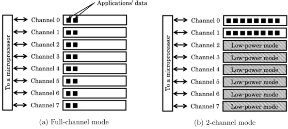
Compute-intensive applications do not require the high bandwidth realized by many chan-nels because their access requests are intermittent and not frequent. However, as shown in the re-sults in Section 1.3, some of compute-intensive applications cannot exploit the low-power modes. These applications’ data are distributed to all the channels, and these intermittent requests to the data also widely spread over the channels. The frequency of these requests is small but not enough to allow the channels and their components to enter the self-refresh modes. Therefore, the energy consumption of the memory system increases even in the case of compute-intensive applications.
Figure 5 shows the concept of our approach to solve the above problem. Figure 5a is a
mode that can fully use all the channels, thefull-channel mode. In this mode, the applications’
data are distributed to all the eight channels. In this mode, the memory system can achieve the highest memory bandwidth. On the other hand, Fig. 5b is a mode that can use a limited number of channels. In this case, all the data are stored into Channels 0 and 1, and only these channels are accessed. To realize such a situation, the data in Channels 2 to 7 are migrated to Channels 0 and 1. Then, Channels 2 to 7 are not accessed. Therefore, these channels can move to the self-refresh mode. The compute-intensive applications can keep the high performance even though the memory system with limited channels reduces the bandwidth.
(a) Full-channel mode (b) 2-channel mode
Figure 5. Full-channel mode for high performance and 2-channel mode for low power
This is because, when switching the schemes, the data stored in the memory system have to be migrated to the locations mapped by the newly-switched scheme.
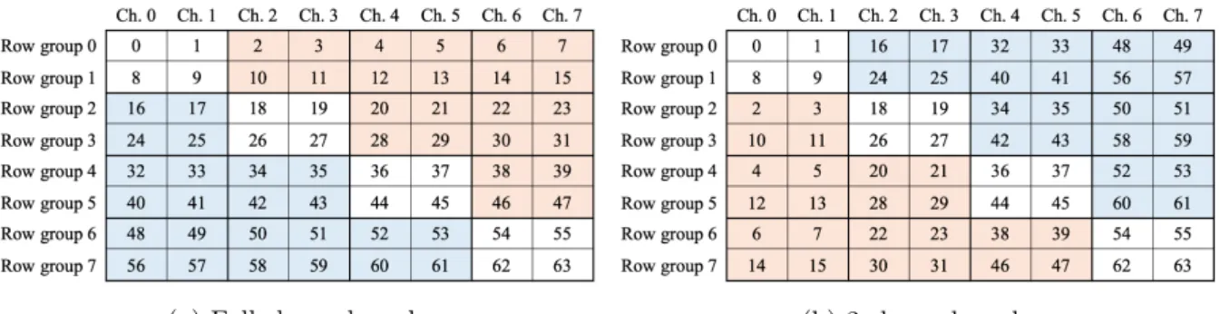
To satisfy the above conditions, this paper considers variations of address-mapping schemes inspired by matrix transposition. By the matrix transpositions, the elements standing in one row are rearranged as those in one column. Such rearranging can be applied to the data migrations to distribute the data over the channels or gather the data into one channel. Figure 6 shows two address-mapping schemes in the case of an 8-channel memory system, and how these schemes
map the sequential addresses to channels and groups of rows, calledrow groups. Figure 6a is the
scheme for the full-channel mode. Figure 6b is for the 2-channel mode. When the addresses in each scheme are regarded as items in a matrix, those of the 2-channel mode can be generated by transposing those of the full-channel mode by 2x2 sub-matrices. The orange and blue areas in the figures show where the 2x2 sub-matrices are exchanged.
These schemes can satisfy the requirement to realize the channel modes. If the memory requests are based on a sequential access pattern, the requests are distributed, and the accessed channel is changed for each request in Fig. 6a. On the other hand, in the 2-channel mode in Fig. 6b, the sequential access requests firstly go to Channels 0 and 1. After all the data in these channels are accessed, the subsequent requests go to Channels 2 and 3 until all the data in these channels are accessed. Such an access pattern continues to Channels 6 to 7. Focusing on a certain period during execution, two channels are accessed simultaneously. Moreover, to change the channel modes, data are migrated by the pattern of matrix transposition. There is no need to memorize the mapping between physical addresses and locations on the memory system.
(a) Full-channel mode (b) 2-channel mode
Figure 6.Maps of the sequential addresses to the channels and the row groups
Figure 7 shows how a physical address is mapped to the physical location of DRAM. These examples are the cases of switching the full-channel mode and the two-channel mode. In the full-channel mode, the bits of row address, bank address, channel address, and column address are extracted as shown in Fig. 7. The channel address is extracted from the least significant bits except for the column address. In the 2-channel mode, the most significant two bits in the row address are exchanged. Hence, the channel address is generated by using the most significant two bits and the least significant one bit except for the column address. Generally, due to the locality of memory accesses, the lower bits in the physical address are changed easier than the upper bits. Therefore, in the 2-channel mode, the lower one bit of the channel address easily changes, but the upper two bits hardly change. It limits the number of accessed channels to two in a certain period. These address-mapping schemes can be generalized. Here, the number of
the lower bits in the channel address is defined as n. The matrix transposition shown in Fig. 6
0 … 0 1
10 0 … 0
0 00
Column Row
Channel Row-group ID
0 … 0 Bank
Full-channel mode
0 … 0 1
10 0 0 … 0 0 … 0 00
2-channel mode
Figure 7. Address-mapping schemes limiting the number of channels
2.2. Dynamic Data Allocation Mechanism
2.2.1. Hardware organization
To realize switching the channel modes, this paper proposes the dynamic data allocation mechanism. The proposed mechanism is implemented on the memory controller, which is the front-end of accessing the memory system. In the case where the number of channels is large, a lot of channel modes are available, e.g., the 1-channel mode, the 2-channel mode, the 4-channel mode, and the full-channel mode in the case where the number of channels is eight. To suppress the hardware cost to manage these modes, the full-channel mode and another channel mode are considered in this paper.
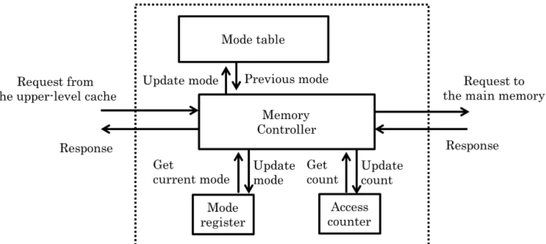
Figure 8 shows the memory controller with the proposed dynamic data allocation
mecha-nism. The memory controller is accompanied with additional components, the mode register,
themode table, and theaccess counter. The mode register indicates which channel mode should be used currently. The preferred channel mode is determined by the number of accesses at a certain period. The controller counts memory requests by using the access counter. The mode table manages which channel mode is used for the previous access to the physical address by memorizing pairs of the physical address and its channel mode. Note that, the proposed mech-anism migrates the data in a unit of row only when the included data are firstly accessed after switching the schemes. This is because it takes a long time to complete migrating all the data to every switching. Therefore, the mode table has to store the pairs for every row.
Access counter Memory
Controller Mode table
Previous mode Update mode
Response
Request to the main memory
Response Update
count Get
count
Mode register
Update mode Get
current mode Request from
the upper-level cache
Figure 8. Dynamic data allocation mechanism: a memory controller with facilities switching
2.2.2. Memory access procedure
The memory controller with the proposed mechanism is placed between the processor and the main memory. The address conversion is done only in the lower layers from the memory controller. Therefore, the processor-side hardware does not need to know whether the data are migrated or not. The memory controller determines the physical location of the address of a memory request by the address-mapping scheme currently selected, and processes the access request.
The detailed procedure to process the memory requests is as follows. If a memory request comes from the processor, the controller knows which is the current mode from the mode register. Next, the controller accesses the mode table based on the physical address to know the mode used in the previous access to that address. If the current mode is different from the previous mode, the data are migrated so that the data can be accessed by the current mode. The mode table is also updated to store the current mode for this physical address. Finally, the memory request is processed by the current mode as the normal memory controller does.
After receiving the data from the main memory, the memory controller knows the channel mode from the mode table when the memory request comes. If the mode is changed from the default mode, here the full-channel mode, the data are sent directly to the processor. If the mode is different from the default mode, the address is reverted to the original one, and the data are sent to the processor.
2.2.3. Hardware overhead of the mechanism
To realize such a migration mechanism, the mode table needs to store the previous address-mapping scheme for each row. In the case where the controller switches two schemes, the mode table should be indexed by a row address, and each entry should store one bit that indicates the mode. In addition, the rows to be swapped should be kept temporarily for the migrations. These costs depend on the configuration of the memory system. The details of the overhead will be discussed in Section 3.
3. Evaluations
3.1. Evaluation Setup
3.1.1. Applications
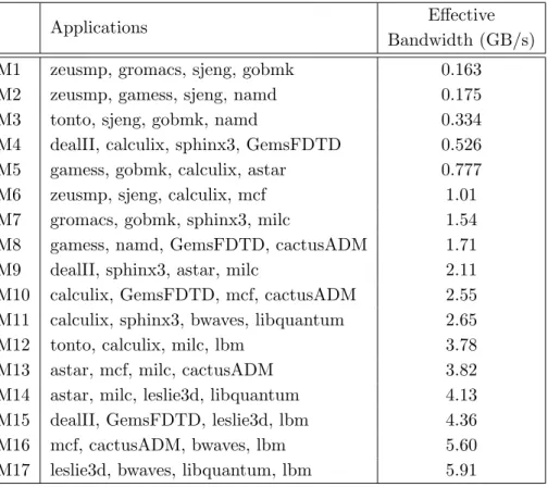
Table 2. Multi-programmed workloads
Applications Effective
Bandwidth (GB/s)
M1 zeusmp, gromacs, sjeng, gobmk 0.163
M2 zeusmp, gamess, sjeng, namd 0.175
M3 tonto, sjeng, gobmk, namd 0.334
M4 dealII, calculix, sphinx3, GemsFDTD 0.526
M5 gamess, gobmk, calculix, astar 0.777
M6 zeusmp, sjeng, calculix, mcf 1.01
M7 gromacs, gobmk, sphinx3, milc 1.54
M8 gamess, namd, GemsFDTD, cactusADM 1.71
M9 dealII, sphinx3, astar, milc 2.11
M10 calculix, GemsFDTD, mcf, cactusADM 2.55
M11 calculix, sphinx3, bwaves, libquantum 2.65
M12 tonto, calculix, milc, lbm 3.78
M13 astar, mcf, milc, cactusADM 3.82
M14 astar, milc, leslie3d, libquantum 4.13
M15 dealII, GemsFDTD, leslie3d, lbm 4.36
M16 mcf, cactusADM, bwaves, lbm 5.60
M17 leslie3d, bwaves, libquantum, lbm 5.91
3.1.2. Parameters of the proposed mechanism
To evaluate the proposed mechanism, the simulation experiment is conducted. This eval-uation supposes that the target system has a 4GB HBM2 module with eight channels as the main memory. The simulation parameters are similar to those of the preliminary experiment in Section 1.3, but the system has four cores with L1 private I/D caches, and the L2 cache is shared among the cores. In this experiment, the proposed mechanism switches two schemes, the full-channel mode that uses eight channels and the 2-channel modes. For the proposed scheme,
two parameters, an interval to switch the modes and the threshold to trigger the switch,should
be determined. The relationships between these parameters and the effectiveness of the proposal are preliminarily evaluated. Based on the results, the threshold that triggers to switch the mode is set to 0.64GB/s, and the interval to change the scheme is 50ms.
The simulation starts by using the full-channel mode, and the proposed mechanism does not change the initial scheme until the first one billion instructions are skipped. After this skipping, the switching function of the proposed scheme is enabled, and the data correction for the evaluation is validated.
bits, the number of entries can be reduced by three-eighths. Therefore, the table size required for this experimental condition is 93KB.
The energy overhead of this mode table is estimated by using CACTI [10] and statistics from the simulator. CACTI can estimate the dynamic read and write energy consumptions and the leakage power of memory arrays. Since the number of accesses to the mode table and the execution time can be estimated by the simulator, the total energy consumption of the mode table can be calculated for each workload. Note that the capacity of the memory array must be
2n bytes in CACTI wherenis a natural number. Therefore, the estimated results of the 128KB
SRAM array are used in this evaluation. The technology node and the transistor model used in this evaluation is 22nm and the Low Standby Power model (LSTP), respectively. Since the number of accesses to the mode table is not so large compared with those to the upper-level caches, the LSTP transistor can contribute to the reduction in the total energy consumption of the mode table.
3.2. Evaluation Results
3.2.1. Performance
In this paper, the performances of the multi-programmed workloads are evaluated by the
weighted speedup [5]. This metric is defined as Equation (1).
W eightedSpeedup=
N
X
i
IP Cshared i
IP Calone i
(1)
Here, IP Cialone means IPC of the i-th application in the case where the i-th application is
executed solely.IP Cishared stands for IPC of that application in the case where the application
runs with all theN applications in the workload together. The higher weighted speedup means
the better performance. Moreover, this metric can fairly assess the workload performance even in the case where one application has a large IPC but the others mark lower IPCs.
0.8 0.85 0.9 0.95 1 1.05
M1 M2 M3 M4 M5 M6 M7 M8 M9 M10 11M M12 M13 M14 M15 M16 M17
Ca
t.
A
Ca
t.
B
AL
L
Category A Category B Average
W
ei
ght
ed
S
pe
edup
BASE Static8ch Proposal
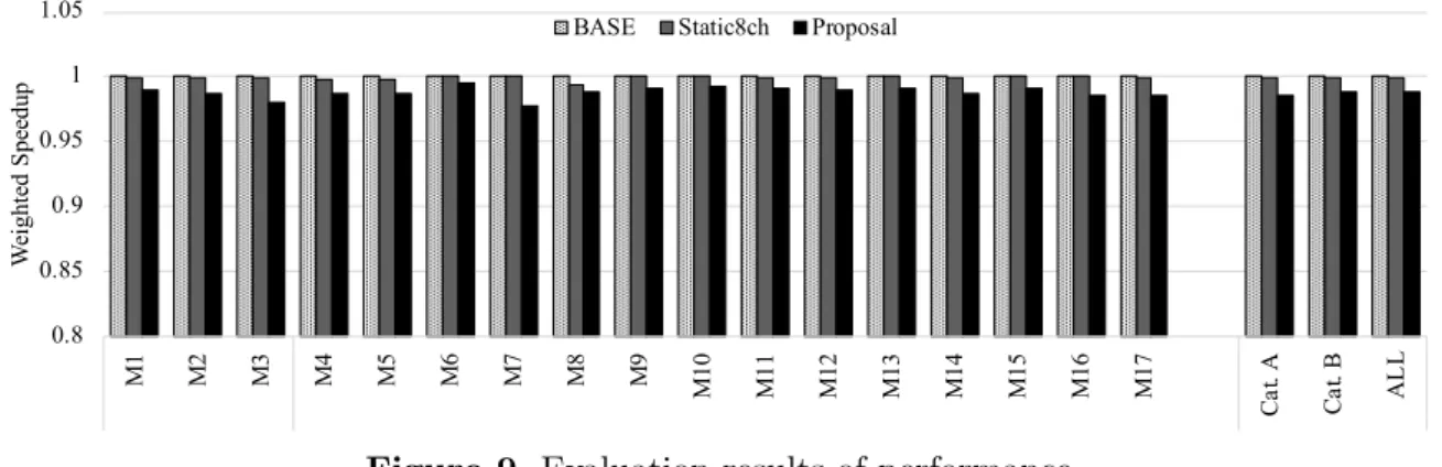
Figure 9. Evaluation results of performance
Figure 9 shows the evaluation results of the performance. The horizontal axis shows the workloads used in this evaluation, and the vertical axis shows the weighted speedup when the
self-refresh mode is not used, calledBASE. The four graphs in one application show the performances
in the case of BASE, Static8ch that always uses the full-channel mode, and Proposal showing
the results of the proposed mechanism.
0.8 0.85 0.9 0.95 1 1.05
M1 M2 M3 M4 M5 M6 M7 M8 M9 M10 11M M12 M13 M14 M15 M16 M17
Ca
t.
A
Ca
t.
B
AL
L
Category A Category B Average
N
or
m
al
iz
ed
E
P
I
BASE Static8ch Proposal ModeTableOverhead
Figure 10.Evaluation results of energy per instruction
performance overheads by the additional latency and the migration costs of the proposed mech-anism. Therefore, the performance of the proposed mechanism does not reach those of BASE and Static8ch.
Comparing the workloads in Category A and those in Category B, there are no remarkable differences. The workloads in the Category A easily switch to the two-channel mode because of the low effective memory bandwidth. Although switching the schemes causes the migration overhead, its performance penalty is not so large compared with those of Category B. Therefore, the impact of the migration overhead of the proposed mechanism on the performance is not significant.
3.2.2. Energy consumption
Figure 10 shows the evaluation results of the energy consumptions. The horizontal axis shows the workloads, and the vertical axis shows the energy per instruction (EPI) normalized
by the results of BASE, which does not use the self-refresh mode. The legend of the graph
is almost the same as that of Fig. 9, but an energy overhead of the mode table is added as
ModeTableOverhead. Note that the energy consumption by the additional memory requests for the migration is already included in that of the proposal.
From Fig. 10, it is observed that the EPIs of the proposed scheme are smaller than those of BASE and Static8ch on average. The proposed mechanism reduces the EPIs by up to 11.8% and 12.0%, and 1.7% and 1.6% on average compared with BASE and Static8ch, respectively. Therefore, the proposed mechanism can contribute to the reduction in the energy consumption by reducing the number of channels.
Focusing on each category, the EPIs of the workloads in Category A are reduced by 9.9% on average. It indicates that the proposed mechanism is effective for these applications, each of which marks the lower bandwidth. On the other hand, for the workloads in Category B, the proposed mechanism cannot reduce the EPIs. This is because the proposed mechanism cannot switch to the 2-channel mode to avoid performance degradation for these workloads.
0.7 0.75 0.8 0.85 0.9 0.95 1 1.05 1.1 0% 10% 20% 30% 40% 50% 60% 70% 80% 90% 100% ze us m p gr om ac s ga m es s tont o sj eng gobm k na m d de al II ca lc ul ix sphi nx3 GemsF
DTD astar mc
f milc ca ct us A D M le sl ie 3d bw ave s li bqua nt um lbm
Category A Category B
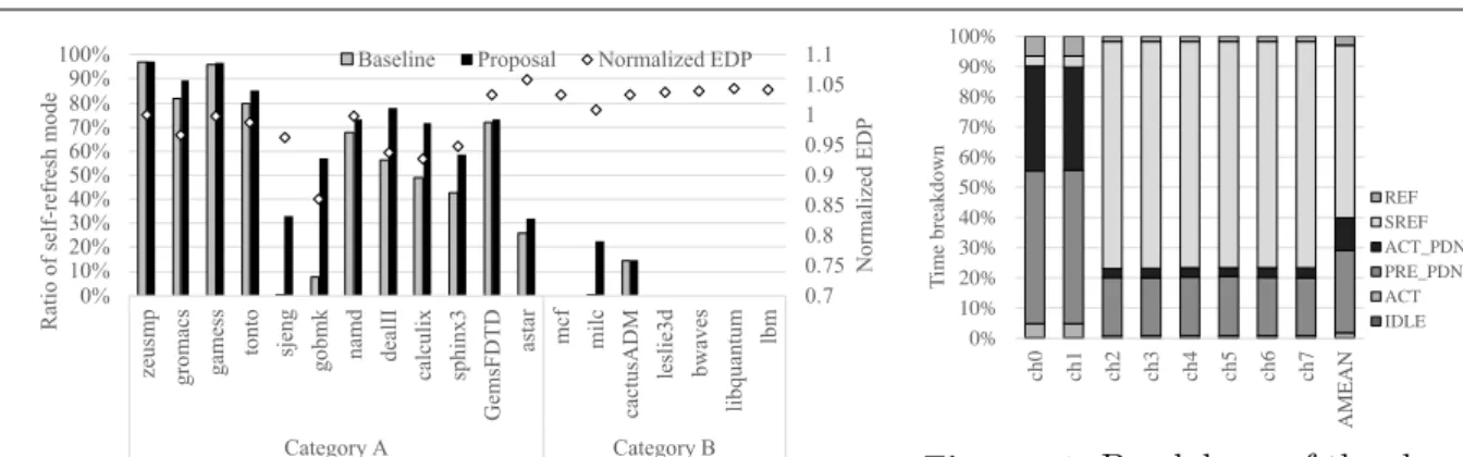
N or m al iz ed E D P R at io of s el f-re fr es h m ode
Baseline Proposal Normalized EDP
Figure 11.The ratio of entering the self-refresh mode
0% 10% 20% 30% 40% 50% 60% 70% 80% 90% 100% ch 0 ch 1 ch 2 ch 3 ch 4
ch5 ch6 ch7
AM E AN T ime b reakd o wn REF SREF ACT_PDN PRE_PDN ACT IDLE
Figure 12. Breakdown of the
chan-nels in each mode
checked every memory access. Since the benchmarks in Category B need many memory accesses, the number of accesses to the mode table also becomes large. Therefore, the energy consumption of the mode table increases.
3.2.3. Mode breakdown
To analyze the effectiveness of the proposed mechanism, this section evaluates the breakdown of the execution time in the single-thread application. Figure 11 shows the total length of the period in the self-refresh mode and their effects. The horizontal axis shows the applications. The left vertical axis and two bar graphs show ratios of the self-refresh mode to the total time. The
two graphs show the ratios of Baseline and Proposal, which are the original address-mapping
scheme and the proposed mechanism, respectively. The right vertical axis and dot graphs show the energy-delay products when using the proposed mechanism, which is normalized by that of Baseline.
From Fig. 11, it is observed that the ratio of the self-refresh mode increases by the proposed mechanism compared with Baseline. This fact indicates that the proposed mechanism actually increases the time in the self-refresh mode, resulting in the energy reduction. The applications, the times of which in the self-refresh mode increase, especially in Category A, can reduce the energy-delay products. Otherwise, in Category B, the energy-delay products do not decrease. As a result, the energy-delay products slightly increase due to the performance degradations by the performance overheads of the proposed mechanism.
Among these applications, the proposed mechanism is most beneficial to the benchmark gobmk. To analyze the details of this application, Fig. 12 shows the breakdown of the total execution time into times for individual modes in gobmk. The difference from Fig. 4 is that the proposed mechanism is applied. From Fig. 12, it is clear that the time in the self-refresh
mode increases compared with the case in Fig. 4 in the six channels that are ch2toch7 in these
figures. This is the main reason for reducing the energy consumption. On the other hand, the fact
that the ratios of the active mode (ACT) increase in ch0 and ch1 indicates that the proposed
mechanism successfully gathers the frequently accessed data into ch0 and ch1. Although the
time durations of the self-refresh mode of these channels decrease, its effect is not dominant for the total energy consumption.
Conclusions
ranks in the channels cannot exploit the lower-power modes, especially the self-refresh modes. To solve this problem, this paper proposes a dynamic data allocation mechanism for many-channel memory systems. The proposed mechanism switches multiple address-mapping schemes. One scheme is for limiting the number of accessed channels to reduce the energy consumption. The other scheme is to fully exploit all the channels to obtain the higher performance. The evaluation results show that the proposed mechanism can reduce the energy consumption by up to 11.8% and 1.7% on average.
As future work, the variations of channel modes by different address-mapping schemes should be explored. The proposed mechanism should use more effective channel modes. Furthermore, the proposed mechanism switches only the two modes, however, may become more effective by switching three or more channel modes.
Acknowledgement
This work is partially supported by MEXT Next Generation High-Performance Comput-ing Infrastructures and Applications R&D Program, entitled “R&D of A Quantum-AnnealComput-ing- Quantum-Annealing-Assisted Next Generation HPC Infrastructure and its Applications” and Grants-in-Aid for Early-Career Scientists No. 19K20232.
This paper is distributed under the terms of the Creative Commons Attribution-Non Com-mercial 3.0 License which permits non-comCom-mercial use, reproduction and distribution of the work without further permission provided the original work is properly cited.
References
1. Binkert, N., Beckmann, B., Black, G., Reinhardt, S.K., Saidi, A., Basu, A., Hestness, J., Hower, D.R., Krishna, T., Sardashti, S., Sen, R., Sewell, K., Shoaib, M., Vaish, N., Hill, M.D., Wood, D.A.: The gem5 simulator. ACM SIGARCH Computer Architecture News 39, 1–7 (Aug 2011), DOI: 10.1145/2024716.2024718
2. Bojnordi, M.N., Ipek, E.: Pardis: A programmable memory controller for the DDRx inter-facing standards. In: 39th Annual International Symposium on Computer Architecture. pp. 13–24. IEEE, Portland, OR, USA (Jun 2012), DOI: 10.1109/ISCA.2012.6237002
3. Borkar, S.: Thousand core chips: A technology perspective. In: The 44th Annual De-sign Automation Conference. pp. 746–749. DAC ’07, ACM, New York, NY, USA (2007), DOI: 10.1145/1278480.1278667
4. Chatterjee, N., O0Connor, M., Lee, D., Johnson, D.R., Keckler, S.W., Rhu, M., Dally,
W.J.: Architecting an energy-efficient DRAM system for GPUs. In: IEEE International Symposium on High Performance Computer Architecture (HPCA). pp. 73–84. Austin, TX, USA (2017), DOI: 10.1109/HPCA.2017.58
5. Eyerman, S., Eeckhout, L.: System-level performance metrics for multiprogram workloads. IEEE Micro 28(3), 42–53 (2008), DOI: 10.1109/MM.2008.44
7. Jacob, B., Ng, S.W., Wang, D.T.: Memory Systems: Cache, DRAM, Disk. Morgan Kauf-mann (2008)
8. Jang, J.W., Jeon, M., Kim, H.S., Jo, H., Kim, J.S., Maeng, S.: Energy reduction in consoli-dated servers through memory-aware virtual machine scheduling. Computers, IEEE Trans-actions on 60(4), 552–564 (Apr 2011), DOI: 10.1109/TC.2010.82
9. Lebeck, A.R., Fan, X., Zeng, H., Ellis, C.: Power aware page allocation. ACM SIGOPS Operating Systems Review 34(5), 105–116 (Dec 2000), DOI: 10.1145/384264.379007
10. Li, S., Chen, K., Ahn, J.H., Brockman, J.B., Jouppi, N.P.: Cacti-p: Architecture-level modeling for SRAM-based structures with advanced leakage reduction techniques. In: IEEE/ACM International Conference on Computer-Aided Design (ICCAD). pp. 694–701. IEEE (Nov 2011), DOI: 10.1109/ICCAD.2011.6105405
11. Micron Technology Inc.: Micron MT40A2G4 data sheet (Oct 2015)
12. Sato, M., Chengguang, H., Komatsu, K., Egawa, R., Takizawa, H., Kobayashi, H.: An energy-efficient dynamic memory address mapping mechanism. In: IEEE Symposium on Low-Power and High-Speed Chips (COOL Chips XVIII). pp. 1–3. Yokohama, Japan (Apr 2015), DOI: 10.1109/CoolChips.2015.7158660
13. Tran, K., Ahn, J.: HBM: Memory solution for high performance processors. In: MemCon. Santa Clara, CA, USA (Oct 2014)
14. Udipi, A.N., Muralimanohar, N., Chatterjee, N., Balasubramonian, R., Davis,
A., Jouppi, N.P.: Rethinking DRAM design and organization for
energy-constrained multi-cores. SIGARCH Comput. Archit. News 38(3), 175–186 (Jun 2010), DOI: 10.1145/1816038.1815983
15. Weis, C., Loi, I., Benini, L., Wehn, N.: Exploration and optimization of 3-D integrated DRAM subsystems. IEEE Transactions on Computer-Aided Design of Integrated Circuits and Systems 32(4), 597–610 (Apr 2013), DOI: 10.1109/TCAD.2012.2235125
16. Wilkes, M.V.: The memory gap and the future of high performance memories. SIGARCH Comput. Archit. News 29(1), 2–7 (Mar 2001), DOI: 10.1145/373574.373576
17. Wu, D., He, B., Tang, X., Xu, J., Guo, M.: RAMZzz: Rank-aware DRAM power manage-ment with dynamic migrations and demotions. In: The International Conference on High Performance Computing, Networking, Storage and Analysis. pp. 32:1–32:11. Los Alamitos, CA, USA (Nov 2012), DOI: 10.5555/2388996.2389040
18. Wulf, W.A., McKee, S.A.: Hitting the memory wall: Implications of the obvious. ACM SIGARCH Computer Architecture News 23, 20–24 (Mar 1995), DOI: 10.1145/216585.216588
19. Yamada, Y.: Vector engine processor of NECs brand-new supercomputer SX-Aurora TSUB-ASA. In: HotChips: A Symposium on High Performance Chips. Cupertino, CA, USA
(Aug 2018), https://www.hotchips.org/hc30/2conf/2.14_NEC_vector_NEC_SXAurora_