Contents lists available atScienceDirect
Ceramics International
journal homepage:www.elsevier.com/locate/ceramint
Multi-scale defects in ZnO thermoelectric ceramic materials co-doped with
In and Ga
Anh Tuan Thanh Pham
a,b, Tuyen Anh Luu
c,d, Ngoc Kim Pham
b,e,f, Hanh Kieu Thi Ta
b,e,f,
Truong Huu Nguyen
a,b, Dung Van Hoang
a,b,f, Hoa Thi Lai
b,f, Vinh Cao Tran
a,b, Jong-Ho Park
g,
Jae-Ki Lee
g, Sungkyun Park
h, Ohtaki Michitaka
i, Su-Dong Park
g, Hung Quang Nguyen
j,
Thang Bach Phan
a,b,f,∗aLaboratory of Advanced Materials, University of Science, HoChiMinh City, Viet Nam bVietnam National University, HoChiMinh City, Viet Nam
cCenter for Nuclear Techniques, Vietnam Atomic Energy Institute, HoChiMinh City, Viet Nam dJoint Institute for Nuclear Research, Dubna, Russia
eFaculty of Materials Science and Technology, University of Science, HoChiMinh City, Viet Nam fCenter for Innovative Materials and Architectures (INOMAR), HoChiMinh City, Viet Nam
gThermoelectric Conversion Research Center, Korea Electrotechnology Research Institute, Republic of Korea hDepartment of Physics, Pusan National University, Busan, Republic of Korea
iDepartment of Applied Science for Electronics and Materials, Kyushu University, Japan jInstitute of Fundamental and Applied Sciences, Duy Tan University, HoChiMinh City, Viet Nam
A R T I C L E I N F O
Keywords:
Ga and In dually-doped ZnO Thermal conductivity X-ray techniques
Positron annihilation lifetime Doppler broadening spectroscopy Multi-scale defects
A B S T R A C T
In this work, several X-ray and nuclear analysis techniques were used to examine ZnO materials co-doped with In and Ga, or IGZO materials. X-ray diffraction analysis, energy-dispersive X-ray spectroscopy, and X-ray photo-electron spectroscopy revealed multi-scale defects in the materials. A nanoscale secondary Ga2Zn9O12spinel phase, mesoscale grain boundaries, and atomic-scale lattice defects were detected. The lattice defects included oxygen vacancies, zinc vacancies, and complex defects. Positron annihilation spectroscopy and Doppler broadening spectroscopy provided evidence of interactions between charge carriers and defects sites, which explained the low thermal conductivities of the IGZO materials (κtotal≈3.9 W/mK) at 773 K. This combination of X-ray and nuclear analytical techniques can be viewed as a novel approach for investigating the thermo-electric properties of materials with complex crystal structures that contain atomic-scale voids, nanoscale sec-ondary phases, and mesoscale grain boundaries.
1. Introduction
Thermal conductivity is one of the three important characteristics of thermoelectric (TE) materials, which are used to fabricate TE gen-erators (TEGs) and TE coolers (TECs). The dimensionlessfigure of merit (ZT) of a TE material is estimated to be σS2T/κ, whereσrepresents electrical conductivity, S is the Seebeck coefficient,κrepresents thermal conductivity, T is the absolute temperature, and the productσS2is the power factor (PF). The κ-value in the denominator is the sum of the electronic (κelectron) and lattice (κlattice) thermal conductivities. The PF value in the numerator can be improved. However, the extent to which ZT can be enhanced by increasing PF is limited due to the strong trade-offbetween S,σ, and the carrier concentration [1–3]. Reduction ofκis
limited by natural thermal phonon transport. The lattice component of κ, which depends on the lattice structure of a material, is generally dominant for semiconductors [4]. Controlling the thermal con-ductivities of TE materials has therefore emerged as an effective strategy for achieving good performance. Nanostructure engineering and dopant addition are two approaches for reducing thermal con-ductivity. Nanostructure engineering is performed to shorten the phonon mean free path or to enhance phonon scattering in low-di-mensional materials, such as quantum dots, nanowires, superlattices, and thin films. Dopant addition improves conductivity and reduces thermal conductivity by introducing scattering elements, such as de-fects, nanoprecipitate secondary phases, distortions, and stacking faults.
https://doi.org/10.1016/j.ceramint.2020.01.084
Received 19 November 2019; Received in revised form 2 January 2020; Accepted 9 January 2020
∗Corresponding author. Laboratory of Advanced Materials, University of Science, HoChiMinh City, Viet Nam.
E-mail address:[email protected](T.B. Phan).
Available online 13 January 2020
0272-8842/ © 2020 Elsevier Ltd and Techna Group S.r.l. All rights reserved.
The identification of scattering elements is necessary to achieve good thermoelectric properties. Photoluminescence (PL) spectroscopy, high-resolution transmission electron microscopy (HR-TEM), energy-dispersive X-ray spectroscopy, and X-ray photoelectron spectroscopy (XPS) are used to detect the structural changes induced by the in-troduction of dopants. Nuclear methods, including positron annihila-tion lifetime (PAL) spectroscopy [5] and Doppler broadening (DB) spectroscopy [6], are useful for analyzing materials that contain void defects, such as vacancies, secondary phases, and dislocations. These methods have been used widely and frequently for several decades to study the internal structures of materials with different properties [7–11].
PAL spectroscopy is used to measure the time that elapses between the introduction of a positron into a material from a22Na radioisotope source, which simultaneously emits gamma (γ) rays, and positron-electron annihilation, which also emitsγrays [5,6]. Positrons in doped materials can be rapidly trapped within the grain boundaries of the solid matrix. Positrons are also trapped in defects, such as vacancies and voids, and in doping sites, such as substitutions and interstices. The lifetimes of positrons in these locations are frequently longer than they are in perfect structures [9,11]. DB positron annihilation spectroscopy is often performed by measuring photonic energy around the 511 keV annihilation line. These photons are generated through positron-elec-tron annihilation, and the width and shape of the 511 keV annihilation line are related to the electron momentum distribution and the electron density at annihilation sites [7,8]. PAL spectroscopy is used to obtain information about the local structures around distortion-related lattice defects, which is based on positron lifetime. Doppler broadening of radiation from position-electron annihilation can reveal the density of lattice defects by providing information about the electron momentum distribution around them and about interactions between electrons and the lattice defects. Understanding the lattice structure, lattice defects, and the electron distribution in the lattice and around lattice defects can elucidate the thermoelectric properties of a material, particularly its thermal conductivity.
In this work, a combination of X-ray and nuclear analytical methods was employed to identify and understand the impacts of lattice defects, secondary phase segregation, and bulk densification on reducing the thermal conductivity of doped ZnO bulk materials. ZnO is a well-known and promising large-bandgap TE material. It is non-toxic, eco-friendly, inexpensive, and exhibits high thermal and chemical stability [12,13]. The TE advantage of pure ZnO arises from its thermal stability and relatively high Seebeck coefficient, which is a result of low carrier concentration. However, strong harmonic phonon vibration due to its simple wurtzite structure, its light atomic mass, and strong atomic bonding in ZnO are drawbacks [14] that give rise to a very high thermal conductivity (κ) of ~50 W/mK [15]. Many researchers have attempted to reduce theκvalue of ZnO using one of two strategies, point-defect engineering [16–21] and nanostructure manufacturing [4,22–27]. Most of these efforts have involved doping the ZnO matrix with different elements, which is likely the simplest strategy for controlling the TE parameters of a material simultaneously. For instance, Zhu et al. re-ported that the TE properties of bulk ZnO were significantly enhanced by doping it with a small amount of sulfur [19]. The electrical con-ductivity of the S-doped ZnO bulk was improved, while its thermal conductivity at 373 K was reduced by 20% relative to that of its un-doped counterpart. The lowestκof ~4 W/mK was observed in bulk ZnO0.09S0.01at 973 K. Double-element doping of the ZnO network has been reported to be more effective than doping with a single element [21–26]. Takemoto et al. reported that the introduction of stacking faults into ZnO by doping it with Ga and In reduced its κvalue sig-nificantly to 1.7 W/mK at 773 K [34]. Nanostructure manufacturing is the most promising strategy for designing the next generation of high-performance TE materials [3,35]. Han et al. attributed a significant decrease in the dominantκlatticecomponent ofκin bulk Zn0.98Al0.02O to a reduction in phonon scattering, which was due to nanoprecipitate
formation in powders with different morphologies [4]. They observedκ values of approximately 36, 22, and 8.5 W/mK at 373 K in bulk solids consisting of rods, platelets, and nanoparticles, respectively. The lowest κof ~3.21 W/mK was observed in nanoparticle samples at 1223 K. In another study, Zhang et al. observed a lowκof 2.1 W/mK at 1073 K and a high carrier mobility of 50.7 cm2/V∙s in a bulk Zn
0.98Al0.02O hybrid micro/nanostructure [24].
In this work, point defects, secondary phases, and bulk density were introduced as scattering elements into ZnO materials using Ga and In dopants under various preparation conditions. In and Ga were chosen as dopants due to the electrical conductivity and thermal stability of IGZO materials. Our previous work indicated that compensation for the ionic radii and bond lengths of the Ga and In dopants stabilized the ZnO network, resulting in good thermoelectric performance and stability in the mid-to high-temperature range [13,28,36]. Furthermore, the heavy atomic weights of Ga and In contributed to a reduction in thermal conductivity. Solid state reaction (SSR) sintering [23,30–34,37,38], hot pressing (HP) [39–41], and spark plasma sintering (SPS) [18,24–27] can facilitate secondary phase segregation in host materials. The SSR is relatively simple, cost-effective, and less polluted. The solubilities of Ga and In in the solid solution, which govern secondary phase segregation, can be modified by adjusting the SSR conditions. Thermal transport at grain boundaries can also be modified to reduce thermal conductivity by controlling bulk densification through precursor preparation.
2. Material and methods
2.1. Preparation processes
The IGZO bulk materials were preparedvia solid state reactions using different preparation processes. ZnO (99.9%, Merck), Ga2O3 (99.99%, Sigma-Aldrich), and In2O3(99.99%, Sigma-Aldrich) powders were used as starting materials. The raw powders were mixed to obtain Ga/In in a 4.5/0.5 ratio (at.%). The wet raw powder mixture was ball-milled for 5 hours. The slurry was carefully dried at 120 °C for one day to remove water and divided into three portions. One portion was hy-draulically pressed into rectangular pellets 30 mm in diameter and annealed directly at 1400 °C, then soaked for 3 hours (process 1). The IGZO bulk obtainedviaprocess 1 was designated @bulk1400. A sepa-rate green compact body obtained under the same pressing conditions was calcinated at 1000 °C for 3 hours. The calcined pellet was then ground using an agate mortar and pestle, pressed again, and sintered at 1400 °C (process 2). The IGZO bulk createdviaprocess 2 with pressure-assisted conglomeration was designated @bulk1000-1400. The third portion of the original dried slurry was calcinated at 1000 °C without pressure-assisted conglomeration. Following calcination of the powder mixture, the green compact body was sintered at 1400 °C (process 3) and designated @powder1000-1400. The three IGZO bulk sintering processes are illustrated inFigs. S1a–c. A photograph of the three sin-tered IGZO bulk samples is shown in Fig. S1d, and the volumetric changes due to sintering are compared inFig. S1e. The largest and smallest shrinkages were observed in the @bulk1400 and @bulk1000-1400 samples, respectively. Shrinkage was closely related to the char-acteristics of the IGZO bulk samples. Densification of the IGZO bulk samples, density, and hardness will be discussed in a later section. An undoped ZnO bulk sample was also preparedviathe one-step process (process 1) and used for reference.
2.2. Characterization of the IGZO bulk samples
2.2.1. Thermal and electrical conductivities
The temperature-dependent thermal conductivity (κ) was obtained using Eq.(1).
whereα,ρ, and Cpare thermal diffusivity, density, and heat capacity, respectively. The IGZO bulks were cut into disk-shaped pieces (12 mm in diameter and 1.5 mm in thickness) to measure their thermal diff u-sivity. An LFA-457 MicroFlash Thermal Analyzer (Netzsch, Germany) was used to analyze the thermal diffusivity. The heat capacity was determinedviadifferential scanning calorimetry (DSC) using a DSC 204 F1 Phoenix calorimeter (Netzsch, Germany). The bulk density of each sample was examined using the Archimedes' method.
A ZEM-3 measurement system (ULVAC-Riko, Japan) was employed to record electrical conductivity as a function of temperature. Rectangular slices (10 × 10 × 0.5 mm3) were used for temperature-dependent Hall measurements. The measurements were performed by using an HMS-5500 Hall measurement system (Ecopia, Korea) from 300 to 773 K to determine the carrier concentrations and mobilities of the samples.
2.2.2. Compositional, structural, and morphological properties
A K-Alpha+ XPS spectrometer (ThermoFisher Scientific, USA) equipped with a monochromatic Al-Kα excitation source (hν= 1486.6 eV) was employed to analyze the compositions, oxidation states, and chemical bonding properties of the samples. The crystalline structures of the bulk samples were determined from their powder X-ray diffraction (XRD) patterns, which were collected on a D8 Advance diffractometer (Bruker, USA). A S-4800field-emission scanning elec-tron microscope (FE-SEM, Hitachi, Japan) was used to observe the fractured surfaces of the samples. An H-7593 energy-dispersive X-ray analyzer (Horiba, Japan) was used to determine the elemental com-positions of the bulks. The hardness of each ceramic was measured using a hardness testing machine (Nanovea, USA) equipped with a diamond Vickers indentation probe.
Nuclear analysis was performed to study structural defects and the positions of the dopants within ZnO using a positron annihilation life-time (PAL) spectrometer and a Doppler broadening (DB) spectrometer. The PAL measurements were performed in a fast-fast coincidence configuration using two Ortec plastic scintillation detectors with a time resolution of 220 ps and a radioactive22Na source. The DB measure-ments were performed using an Ortec HPGe detector (USA) with an energy resolution of 1.5 keV equipped with a radioactive207Bi source. The DB spectra were collected from the photopeak at around 511 keV to monitor γemissions generated from annihilation events by using the same22Na radioactive source as the PAL. The above experiments were configured inside a low-background lead box. These nuclear techniques are known to be among the most effective methods for studying the internal structure of various defect materials [9].
3. Results and discussion
3.1. Thermal conductivity
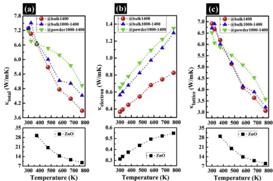
The total thermal conductivity (κtotal) of each bulk IGZO sample and the bulk ZnO reference are depicted as functions of temperature in Fig. 1κtotal included the electron thermal conductivity (κelectron) and lattice thermal conductivity (κlattice). Theκtotalvalues of all the bulk samples decreased monotonically with increasing temperature (Fig. 1a). Theκtotalvalues of the IGZO bulks at 773 K increased from a minimum of ~3.9 W/mK (@bulk1400) to 4.5 W/mK (@powder1000-1400), then to 4.9 W/mK (@bulk1000-1400). Theκtotalvalues of the IGZO bulks were much lower than that of bulk ZnO at 773 K (9.5 W/ mK).
To evaluate thermal conductivity, κtotal can be written as κelectron + κlattice. κelectron depends mainly on the concentration and mobility of the carrier, while κlatticeis an attribute of the crystalline structure. Theκelectroncomponent can be determined according to the Wiedemann-Franz law, shown in Eq.(2).
κelectron= LσT, (2)
whereσis the electrical conductivity of the material, T is the absolute temperature, and L is the Lorentz number (2.45 × 10⁻⁸W∙ΩK−2) [4]. The electrical conductivity of each bulk sample is shown as a function of temperature in Fig. S2 (Supporting Information). The calculated κelectronandκlatticevalues are shown inFig. 1b and c, respectively. Each of the bulk IGZO samples had a higherκelectronvalue and a much lower κlatticevalue than the ZnO sample. Among the IGZO samples, the @ bulk1400 sample had the lowestκelectronandκlatticevalues, particularly at high temperatures. With this combination ofκcomponents, the @ bulk1400 sample had a lowκtotal value that was comparable to the lowest values reported for ZnO-based bulk materials (Fig. 2). We then combined X-ray and nuclear analysis techniques in a new approach to investigate the origins of low thermal conductivity in the IGZO bulks.
3.2. Microcrystalline structures and morphologies
The crystalline structures of the IGZO bulks synthesized using the three processes were evaluatedviaXRD analysis. Their XRD patterns are compared to that of the undoped ZnO bulk reference sample in Fig. 3. Peaks attributed to Ga2O3were observed in the XRD patterns of the raw powders (Fig. S3, Supporting Information), but no significant In2O3content was indicated. This may have been due to the low mixing ratio of In to Ga (0.5/4.5, at.%). After sintering, the host ZnO structure was retained in all of the samples (Fig. 3a). The presence of the Ga2Zn9O12spinel phase (JCPDS No. 50-0448) inFig. 2a was interesting, as some of the ZnO peaks tended to broaden and weaken. Formation of the Ga2Zn9O12spinel as a secondary phase was reported in literature and was strongly indicated in the IGZO bulks sintered at 1400 °C [43–46]. The formation of secondary phases is believed to limit the solubility of Ga in the solid ZnO matrix [21]. Although no characteristic peaks were observed, we could not rule out the formation of secondary phases that contained In Refs. [38,47,48]. The spinel phases relating to Ga and/or In are also known as low-thermal-conductivity structures [49,50].
An obvious difference between the pattern of the sample obtained viathe one-step process (@bulk1400) and those prepared by two-step processes (@bulk1000-1400 and @powder1000-1400) was observed around the (002) peak (Fig. 3b). The predominant orientation of the (100) and (101) planes of ZnO in the IGZO bulks tended to shift towards smaller angles (2θ) relative to those of the bulk ZnO reference. The largest shift in 2θwas observed in the pattern of the @bulk1000-1400 sample. This strongly suggested substitution of Zn2+by In3+, which had a larger ionic radius. A clear peak at (2θ) 35.17° corresponding to the (118) plane of the Ga2Zn9O12spinel phase tended to reduce the intensity of the ZnO (002) peak. The degree of segregation of the spinel phase in the IGZO bulks could be estimated by comparing the re-presentative peaks of the Ga2Zn9O12(118) and ZnO (002) planes, as shown inFig. 3c. The ratio of the relative intensities of the spinel (118) and ZnO (002) peaks indicated that the proportion of the spinel phase was lowest in the @bulk1000-1400 bulk sample and highest in the @ bulk1400 bulk sample. The proportion of the spinel phase in the @ powder1000-1400 sample fell between those of the other samples. Consistent with the observed shift in 2θ, the one-step preparation process induced strong segregation of the spinel phase, while the two-step preparation processes greatly facilitated Zn2+substitution by do-pant ions with little segregation of the spinel phase.
in the (002) direction decreased from 65.8 nm in bulk ZnO to 16.2 nm, 22.8 nm, and 32 nm in the @bulk1400, @bulk1000-1400, and @ powder1000-1400 samples, respectively. This was attributed mainly to the formation of the Ga2Zn9O12spinel phase in the host ZnO structure. The high degree of spinel phase segregation in the @bulk1400 sample strongly suppressed grain growth, and the crystal sizes in the @ bulk1000-1400 and @powder1000-1400 samples were larger than those in the @bulk1400 sample.
The crystalline structure of the @bulk1400 sample was confirmed in our HR-TEM observations. The HR-TEM image in Fig. 3d shows the dominant (100) and (101) planes. The obvious spotty rings in the se-lected area electron diffraction (SAED) pattern (Fig. 3d, inset) were indicative of a polycrystalline sample. However, the (002) plane could not be clearly identified, which was consistent with restricted growth in the (002) direction due to spinel phase segregation.Fig. 3e indicated the presence of the Ga2Zn9O12spinel phase in the characteristic (118) orientation, which was in excellent agreement with the XRD results. Development of the spinel phase was thus strongly promoted in the one-step preparation process, while the two-one-step processes enhanced the solubility of the dopants in the solid and promoted grain growth in the
IGZO bulks.
To understand the influence of the preparation process on grain growth and spinel phase segregation, the fractured surface morpholo-gies of the IGZO bulks were observedviaFE-SEM. The FE-SEM micro-graphs are shown inFig. 4. The @bulk1400 sample had a highly den-sified structure, but it was not homogeneous (Fig. 4b). The insets in Fig. 4b, d, and 4f show pores with diameters ranging from hundreds of nanometers to several micrometers. The surface morphology of the @ bulk1400 sample was consistent with extensive spinel phase formation, as indicated in the XRD results. The high degree of densification in the bulks could be explained in terms of grain boundary diffusion. Boundary diffusion, or the migration of atoms along grain boundaries, led to densification during the sintering process. Grain growth was promoted by atomic transfer across the boundaries, a process called volume diffusion [52]. Small crystalline grains created a large number of grain boundaries, so boundary diffusion predominated in the @ bulk1400 sample.
The compositions of the samples were quantifiedviaenergy dis-persive spectroscopy (EDS). The EDS spectrum of the @bulk1400 sample is shown in Fig. 4g. Elemental mapping of the @bulk1400 sample (Fig. 4h) showed an inhomogeneous distribution of elements, particularly Ga. This was additional evidence of a spinel phase, such as Ga2Zn9O12spinel, in the ZnO network. EDS mapping also indicated that the spinel phase was predominantly localized near pores and at grain boundaries. Due to the high density of small pores in the IGZO bulk sample prepared by the one-step process, the spinel phase was dis-tributed throughout its entire crystalline network. The close-packed structure of the @bulk1400 sample is illustrated inFig. 5, which shows the dense spinel phase at the grain boundaries.
Despite the low degree of densification, the two-step preparation processes yielded IGZO bulk samples with homogeneous morphologies. This was attributed to good incorporation of the dopants into the ZnO matrix and smaller proportions of the spinel phase in the samples, as indicated in the XRD results. There were interesting differences be-tween the morphologies of the IGZO bulks preparedviathe two-step processes. The @bulk1000-1400 sample (Fig. 4d) was highly porous, while the @powder1000-1400 sample exhibited intermediate porosity (Fig. 4f). Jood et al. reported that a highly porous morphology in bulk ZnO was due to nanostructural refinement with In doping [12]. Fig. 1.Thermal conductivities (κ) of the IGZO and reference ZnO bulks: (a)κtotal, (b)κelectron, (c)κlattice.
However, the effect of In doping on the morphologies of the IGZO bulks could be neglected in our work, because the In2O3content of the raw powder mixture did not vary. Most of the variations in porosity may have arisen from differences between the particle sizes in the precursor powders. Particles in the precursor powder of the @bulk1400 sample (Fig. 4a) were much smaller than particles in the @bulk1000-1400 (Fig. 4c) and @powder1000-1400 (Fig. 4e) precursor powders. It should be noted that sinteringfine particles can easily result in strong
anisotropy and agglomeration in bulk ZnO [53]. The @bulk1400 sample obtained fromfine precursor particles was nanostructured and had a dense morphology with a high degree of spinel phase segregation. In contrast, calcination at 1000 °C in the two-step processes facilitated the formation of large precursor particles. The large particles had small surface areas, which gave rise to many large interstitial pores in the IGZO bulks (Fig. 5). Furthermore, calcination is also thought to enhance substitution of Zn2+by Ga3+and In3+. Below 1250 °C, the reaction in Fig. 3.(a) Large-scale and (b) small-scale XRD patterns; (c) relative intensity ratios of the Ga2Zn9O12(118) and ZnO (002) peaks, including thec/aratios and mean crystal sizes of the reference ZnO and the IGZO bulks synthesizedviadifferent processes. (d)–(e) Typical HR-TEM images of the @bulk1400 sample.
the Ga2O3–In2O3–ZnO mixture proceeds quite slowly [46]. This would suggest that substitution is preferred over the formation of homologous compounds like the Ga2Zn9O12 spinel phase. The @bulk1000-1400 sample was highly porous, because densification and segregation of the spinel phase were minimal.
The porosity of the @powder1000-1400 sample was intermediate between those of the @bulk1400 and @bulk1000-1400 samples. Without pressure-assisted calcination, the spaces between the precursor particles were large, and the number of grain boundaries was small. This implied that grain growth was inhibited in the @powder1000-1400 sample. As a result, particles in the @powder1000-@powder1000-1400 sample were larger than the particles in the @bulk1400 sample, but smaller than the particles in the @bulk1000-1400 sample. Therefore, the @ powder1000-1400 sample contained less of the spinel phase than the @ bulk1400 sample and underwent more densification than the @ bulk1000-1400 sample. Unlike spinel phase segregation throughout the crystalline network of the @bulk1400 specimen, local segregation of grains in the @powder1000-1400 bulk sample led to the formation of agglomerates tens of micrometers in diameter. This is illustrated in the insets ofFigs. 4f and 5.
Differences between densification in the IGZO bulks were also in-dicated in the density and hardness tests, as shown in Fig. S5 (Sup-porting Information). The densities and hardnesses of the IGZO bulks obtained viathe one- and two-step preparation processes were quite different. The densities of the @bulk1400, @bulk1000-1400, and @ powder1000-1400 samples were respectively 91.0%, 82.0%, and 79.8% of the standard theoretical density (TD) of ZnO (5.606 g/cm3) [54]. This was consistent with the high degree of densification in the @ bulk1400 sample indicated by SEM and the low degree of densification in the @bulk1000-1400 and @powder1000-1400 samples. The hard-ness values of the bulks were consistent with their measured densities. The @bulk1000-1400 sample had the highest porosity, resulting in the lowest hardness among the samples. However, it was still slightly denser than the @powder1000-1400 sample. This could be explained by weight loss due to volatilization of the constituent oxides during preparation. ZnO has a much higher vapor pressure than In2O3and Ga2O3powders [38,55]. Without pressure assistance during calcination at 1000 °C, the powder lost much more weight than the sample sub-jected to pressure-assisted calcination, because the small particles had a large surface area. This could be why the density of the
@bulk1000-1400 was slightly higher than that of the @powder1000-@bulk1000-1400 sample. Thefirst calcination step at 1000 °C mainly promoted grain growth and the incorporation of dopants into the ZnO network. Subsequent sintering at 1400 °C strongly actuated bulk densification. The solid solubility limit was reached rapidly in the one-step preparation process, leading to formation of the spinel phase and significant bulk densifi -cation. The two-step preparation process had a higher solid solubility limit and resulted in less bulk densification.
3.3. X-ray photoelectron spectroscopy
2p3/2core level could have been due to an enhanced valence electron screening effect among Zn2+ ions. Consequently, the higher binding energy of the ZnIpeak (1021.9 eV) could be attributed to Zn2+in ZnO and Ga2Zn9O12. The integrated peak intensity ratios of the Zn2p3/2core level components are listed inTable 1. The ratio of ZnIto the total peak intensity for the @bulk1000-1400 sample was the smallest, followed by those of the @powder1000-1400 and @bulk1400 samples. The oppo-site trend was observed in the ratio of (ZnII+ ZnIII) to the total peak intensity. These results suggested a reduction in the percentage of Zn in Ga2Zn9O12and an increase in Zn2+substitution by the dopant ions in the @bulk1000-1400 sample. In contrast, the @bulk1400 sample ex-hibited the highest degree of spinel phase segregation and the lowest amount of Zn2+substitution.
The asymmetric peaks in the Ga 2p3/2core level spectrum could be resolved into two peaks, GaI(1117.3 eV) and GaII(1118.3 eV) (Fig. 6b). The dominant GaIpeak had a lower binding energy, which fell between those of metallic Ga (1116.4–1116.7 eV) and Ga2O3 oxide (1118–1118.3 eV) [57,61,62]. Therefore, the GaIpeak was ascribed to Ga3+at Zn2+substitution sites. On the other hand, the Ga
IIpeak at the higher binding energy could be attributed to Ga2O3in the Ga2O3(ZnO)9 spinel phase. The In 3d5/2core level spectrum (Fig. 6c) was similarly deconvoluted into InI(443.7 eV) and InII(444.6 eV) peaks, which were representative of In3+at Zn2+substitution sites and In3+in the oxide-related spinel phase, respectively [58,63]. Like the ZnIcomponent of Zn 2p3/2, variations in the GaII/GaIand InII/InIratios (Table 1) indicated good Zn2+substitution by dopant ions in the @bulk1000-1400 sample. The segregation of the spinel phase was the highest in the @bulk1400 sample, and the @powder1000-1400 sample was intermediate between the two.
Changes in the cationic binding states also resulted in variations at the O 1s core level. The deconvoluted O 1s spectrum contained OI (~530 eV), OII(~531 eV), and OIII(~532 eV) peaks. The OIpeak is characteristic of O2−in stochiometric ZnO. The OIIpeak was ascribed to O2−in non-stochiometric ZnO with oxygen vacancies, while the OIII peak was attributed to adsorbed O2− [64]. Zn2+ ions in the ZnO
structure were mainly located in tetrahedral [ZnO4] sites with four Zn–O bonds, whereas Ga3+ions in the Ga
2O3(ZnO)mstructure occupied octahedral [GaO6] sites [60]. During sintering in the two-step pre-paration processes, some of the Ga3+ ions in [GaO
6] sites in the Ga2Zn9O12 spinel that formed in the calcination step transferred to tetrahedral [GaO4] sites in ZnO. This increased the concentration of oxygen vacancies, which was consistent with variations in the OII/OI ratio (Table 1). This result also suggested that Ga solubility in ZnO was enhanced in the two-step preparation processes. Changes in the OIII/OI ratio were insignificant, which might have been due to limited O2− adsorption during sintering at 1400 °C.
3.4. Positron annihilation spectroscopy
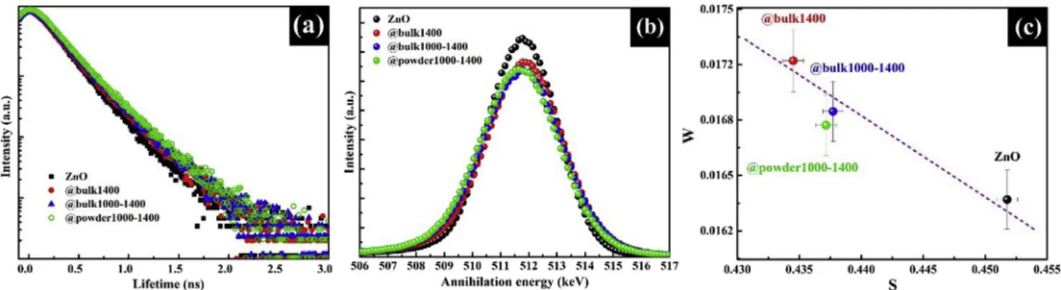
The X-ray methods discussed in sections3.2 and 3.3were used to identify segregation of the spinel phase, the types of point defects, and the level of densification in the investigated samples. We performed positron annihilation (PAL) measurements to identify the predominant defects and to determine the size of defects that induced local structural distortion. PAL also revealed interactions between the defects and charge carriers and local structural distortion that could influence the thermoelectric properties of the IGZO bulks [65,66].
The PAL spectra of the samples inFig. 7a were clearly different. Analysis of the PAL spectra was performed with the LT v.9 program [67] to determine the individual lifetimes of positrons, which were si-milar to those in vacancies. The results suggested that all three pre-paration processes generated very large numbers of vacancies in the bulk samples, which led to the saturation of positron trapping centers. Alternatively, the electron densities in positron annihilation sites, in-cluding vacancies, substitutions, and interstitial sites, may not have been significantly different.
Doppler broadening (DB) measurements (Fig. 7b and c) and electron momentum analysis (Fig. 8) were performed to investigate these pos-sibilities. Analysis of the PAL spectra showed that the measured posi-tron lifetimes in the ZnO, @bulk1400, @bulk1000-1400, and @ Fig. 6.Deconvoluted XPS spectra of (a) Zn 2p3/2, (b) Ga 2p3/2, (c) In 3d5/2, and (d) O 1s core levels of the IGZO bulks.
Table 1
Integrated intensity ratios of deconvoluted component peaks of Zn2p3/2, Ga2p3/2, In3d5/2and O1s core levels (%).
Samples Zn2p3/2 Ga2p3/2 In3d5/2 O1s
ZnI/total (ZnII+ZnIII)/total GaII/GaI InII/InI OII/OI OIII/OI
@bulk1400 31.1 68.9 48.4 38.3 35.1 14.1
@bulk1000-1400 23.8 76.2 33.7 23.2 50.8 18.5
powder1000-1400 samples were 194.8, 214.8, 216.7, and 220 ps, re-spectively (Table 2). These lifetimes were consistent with previously reported values. For example, Sharma et al. [10] found the theoretical and experimental positron lifetimes in individual Zn2+vacancies in ZnO (VZn) to be 196 ps and 201 ps, respectively. These values were similar to the experimental value (~189 ps) reported by Chen et al. [68]. Brauer et al. [69] reported experimental and theoretical positron lifetimes in VZn sites that ranged from 194 to 217 ps. The range of values might have been due to small variations in the electron density. In our work, there was a high likelihood of substitution by Ga3+ions in occupied Zn2+sites (V
Zn). This was because the ionic radius Ga3+was smaller than that of Zn2+, so Ga3+ions might have been present in the interstitial sites of ZnO crystals [70]. Even though its ionic radius was larger than that of Zn2+, the same would be true for In3+if a sufficient amount of the energy supplied during calcination at 1000 °C was ab-sorbed [47]. Thus, Ga3+ substitution and In3+in interstitial sites in ZnO could reduce the electron density at VZnsites. The attractive force between the trivalent ions and nearby electrons was stronger than that between divalent Zn2+ions and nearby electrons, leading to a slight increase in the positron lifetime as reported by Brauer et al. [69]. Based on these results, we concluded that the ZnO, @bulk1400, and @ bulk1000-1400 preparation processes produced only VZn sites. Va-cancies may have been present in both the VZnand Zn–O (VZn-O) sites in the @powder1000-1400 sample. This could explain the longer positron lifetime of ~220 ps in this sample, which was consistent with pre-viously reported values [69]. Single positron lifetimes in the vacancies of all samples provided strong evidence to support our interpretation of
the XRD results (Fig. 3), from which the average crystal sizes of the IGZO grains were determined. We also concluded that the preparation processes produced IGZO grains with characteristic sizes that exceeded the diffusion pathlength of thermalized positrons (~50 nm) [71,72]. Thus, positrons could not diffuse to the surfaces of IGZO grains for positron-electron annihilation in voids or vacancy clusters [10].
DB analysis is often based on two parameters, S and W. The S parameter is defined as the ratio of the area under the center of the photopeak to the total area under the curve. The S parameter is often used to identify small transfers of momentum to annihilation with va-lence electrons. The W parameter is calculated from the ratio of the areas of the wing regions on both sides of the photopeak to the total peak area. W is a measure of more perturbed electrons in a material, such as core electrons, which have higher momenta [8]. Changes in S are thus attributed to the contribution of vacancies, whereas W contains information about the chemical environments of positron annihilation sites in the material. The highest and lowest S and W values for bulk Fig. 7.Positron annihilation measurements of the samples: (a) positron lifetime spectra, (b) Doppler broadening spectra of the annihilation energy, and (c) cor-relation plot of the Doppler broadening parameters (S and W).
Fig. 8.Ratio curves obtained from the Doppler broadening spectra of the bulks: (a) ratio to silicon, (b) ratio to the ZnO reference. (For interpretation of the references to colour in thisfigure legend, the reader is referred to the Web version of this article.)
Table 2
Positron lifetimes (τ) and Doppler broadening parameters (S, W) of ZnO and IGZO.
Samples τ(ps) S (10−4) W (10−4)
ZnO (Table 2) indicated a very high concentration of vacancies and a characteristic chemical environment in this sample. The influence of the preparation processes on the DB parameters of the other bulk samples suggested some interesting phenomena. For instance, the one-step preparation process for the @bulk1400 sample yielded the lowest S value (4345.1 × 10−4) and the highest W value (171.8 × 10⁻⁴). The two-step preparation processes for the @bulk1000-1400 and @ powder1000-1400 samples yielded nearly equal S values of 4377.2 × 10−4and 4371.6 × 10−4and W values of 168.8 × 10⁻⁴and 168.0 × 10⁻⁴. The obtained S values suggested that the one-step preparation process produced fewer vacancies than the two-step pro-cesses. However, the W values implied that a complex chemical en-vironment was generated by the one-step preparation process. The re-sulting chemical environment contained a higher proportion of the spinel phase, which was also indicated in the XRD results. These dif-ferences led to variations in the thermoelectric properties of the bulk samples in this study.
In addition to providing information about defects and chemical environments, the DB parameters are often used to evaluate defect morphology through the construction of a S and W correlation plot (Fig. 7c). Variations in S and W inFig. 7c were approximately linear for the ZnO, @bulk1400, and @bulk1000-1400 samples. However, the @ powder1000-1400 plot went beyond the linear range. Hence, we con-cluded that only VZnsites were present in the ZnO, @bulk1400, and @ bulk1000-1400 samples. VZnand VZn-Osites existed simultaneously in the @powder1000-1400 sample, which was in agreement with the PAL results.
Electron momentum ratio curves were constructed for all of the samples and compared to those of silicon and ZnO to evaluate the roles and positions of the dopants in ZnO. The curves of the measured bulk samples in Fig. 8a exhibited characteristic peaks at an electron mo-mentum (PL) near 15 × 10−3moc. These were due to the contribution of 2p electrons on oxygen atoms during annihilation in VZnsites [73]. This confirmed the presence of VZnsites, which trapped positrons and led to their annihilation with electrons on O atoms in surface defects. The intensity of the PLpeak of the @bulk1400 sample near the dashed line in Fig. 8a was lower at 11 × 10−3 moc. This implied that the vacancy concentration in this bulk sample was lower than those in the @bulk1000-1400 and the @powder1000-1400 samples [8]. The structures of the internal peaks inFig. 8a are magnified inFig. 8b. Two characteristic peaks appeared in the regions from 14 × 10−3 to 20 × 10−3moc and from 20 × 10−3to 27 × 10−3moc in the curve of the @powder1000-1400 sample. In the curves of the other two samples, only one peak was observed between 14 × 10−3and 27 × 10−3moc. The separation of thefirst peak between 14 × 10−3and 20 × 10−3 moc in the @powder1000-1400 sample curve suggested the simulta-neous annihilation of positrons with both 2p and 3d electrons in O and Zn atoms in VZn-Osites. These results confirmed the existence of both types of vacancy in this bulk sample.
Pasang et al. [8] reported on the role of dopants in decreasing the concentration of vacancies in ZnO. We found that Ga3+, which had a smaller ionic radius than Zn2+, could substitute at V
Znsites and enter interstitial sites in ZnO. This reduced the concentration of VZn sites, while the larger ionic radius of In3+allowed it to enter interstitial sites in ZnO. However, it was noted that our samples were sintered at a high temperature. In3+could thus absorb enough thermal energy to sub-stitute in a significant number of VZnsites instead of entering only in-terstitial sites in ZnO. It was also interesting to note that part of the distribution in the @bulk1400 sample curve (Fig. 8b) exceeded unity. This meant that in the one-step preparation process for the @bulk1400 sample, a portion of Ga3+and In3+remained in interstitial sites after substitution at VZn sites was complete. In other words, the two-step preparation processes for the @bulk1000-1400 and @powder1000-1400 samples transferred most of the dopants to vacancies during cal-cination. The differences between the preparation processes resulted in differences between the defect energy levels in the band regions.
Consequently, conduction in the @bulk1400 sample differed from conduction in the @bulk1000-1400 and @powder1000-1400 samples [8].
3.5. Explanation for low thermal conductivity
Based on the results of structural analysis, three factors influenced electron transport in the samples: lattice defects (VZn, VZn-O), the pre-sence of the spinel phase, and bulk densification. Compared to the other IGZO samples, the @bulk1400 sample contained a lower density of lattice defects (VZn). This was based on its shorter positron lifetime. The spinel phase was more abundant in the @bulk1400 sample, because the lower density of lattice defects (VZn) and partial substitution of Ga3+ and In3+in interstitial sites contributed to the formation of the spinel phase. Finally, the solid solubility limit was reached rapidly in the one-step preparation process for the @bulk1400 sample. This resulted in the formation of the spinel phase and significant bulk densification, while the two-step preparation processes for the @bulk1000-1400 and the @ powder1000-1400 samples increased the solid solubility limit and re-duced bulk densification.
Theκelectronvalues of the IGZO bulks were higher than that of the ZnO sample. This was due to higher carrier concentrations in the IGZO samples, which was confirmed in the temperature-dependent Hall measurements (Fig. 9). Regardless of temperature, the @bulk1400 sample consistently had the lowestκelectronvalue. This could be par-tially attributed to its dopant-induced carrier concentration. The sam-ples preparedviaa two-step process exhibited more Zn2+substitution by Ga3+and In3+than the bulk sample prepared in one step.
The electron thermal conductivity was defined as LσT. The carrier concentrations measured at high temperatures were nearly identical in all of the investigated samples (Fig. 9). Therefore,κelectronwas strongly dependent upon carrier mobility, which was influenced by the lattice structure. These results were highly consistent with the results of structural analysis. The lowerκelectronvalue of the @bulk1400 sample could be attributed to scattering due to lattice defects (VZn), the grain boundaries of small grains, a high-density structure, and the spinel phase interface. The κelectron values of the @bulk1400, @bulk1000-1400, and @powder1000-1400 samples at 773 K were 0.83, 1.30, and 1.35 W/mK, respectively.
Theκlatticevalues of all the samples tended to decrease with in-creasing temperature due to increased phonon scattering. Theκlattice values of the IGZO bulks were much lower than that of the ZnO sample.
This was attributed to the dopants and related spinel phase segregation. Likeκelectron, the thermal conductivity of the lattice (κlattice) in the @ bulk1400 sample was the lowest of the IGZO samples. The two major differences between this sample and the others were spinel phase seg-regation and densification. While bulk densification facilitated phonon vibration and thermal transport, segregation of the spinel phase in-hibited transport. The @bulk1400 sample had the lowestκlatticevalue, even though densification was greatest in this sample. This suggested that the influence of the spinel phase in reducing thermal conductivity in the lattice was greater than that of densification. Consequently, the @bulk1400 sample had the lowestκlatticevalue among the IGZO bulks at 773 K (~3.06 W/mK). The @powder1000-1400 and @bulk1000-1400 samples had κlatticevalues of 3.22 W/mK and 3.58 W/mK, re-spectively, at 773 K (Fig. 1c). We noted that theκlatticevalue of each IGZO sample was lower than itsκelectronvalue (Fig. 1b and c). There-fore,κelectronappeared to be influenced more by structural changes than κlattice.
4. Conclusions
In this work, we introduced a novel approach by combining X-ray and nuclear methods to analyze the structural properties associated with thermal conductivity in ZnO materials co-doped with In and Ga. The XRD and XPS analyses revealed the formation of the Ga2Zn9O12 spinel phase. The one-step preparation process strongly promoted for-mation of the spinel phase and densification, while the two-step pro-cesses increased the solubility of the dopants in the solid phase. The two-step processes resulted in less densification, or higher porosity, and less spinel phase segregation. EDS mapping indicated that the spinel phase was localized primarily near pores and at grain boundaries. The nuclear analytical methods clearly supported the results obtained using X-ray methods. The dominant defects, defect densities, and the origin of electrons annihilated at defect sites were determinedviaPAL and DB spectroscopy. Based on the positron lifetimes in the samples, VZndefects were present in the ZnO, @bulk1400, and @bulk1000-1400 samples. Both VZnand Zn–O (VZn-O) vacancies may have been present in the @ powder1000-1400 sample, as it had a longer positron lifetime of ~220 ps. DB analysis showed that the one-step preparation process produced fewer vacancies, while segregation of the spinel phase was more pronounced than it was in the two-step processes. Electron mo-mentum analysis showed that the 2p electrons of oxygen atoms parti-cipated in the annihilation process at VZndefect sites in all of the bulk samples.
The low thermal conductivity of the @bulk1400 sample prepared viathe one-step process was elucidated through structural analysis. Its lower electron thermal conductivity (κelectron) was due to scattering at lattice defects (VZn), the grain boundaries of small grains, a high-density structure, and spinel-phase interfaces. The @bulk1400 sample also had the lowest lattice thermal conductivity (κlattice), although it was the densest sample. While bulk densification facilitated phonon vibration and thermal transport, segregation of the spinel phase inhibited trans-port. This suggests that the spinel phase has a greater impact than densification on reducing thermal conductivity in the lattice.
Our results demonstrate that the combination of X-ray and nuclear analytical techniques can be treated as a novel approach for in-vestigating the thermoelectric properties of materials that contain atomic-scale lattice defects, nanoscale secondary phases, and mesoscale grain boundaries.
Declaration of competing interests
The authors declare that they have no known competingfinancial interests or personal relationships that could have appeared to influ-ence the work reported in this paper.
Acknowledgement
This work was supported by the Vietnam Ministry of Science and Technology under grant numberĐTĐL.CN-23/18.
Appendix A. Supplementary data
Supplementary data to this article can be found online athttps:// doi.org/10.1016/j.ceramint.2020.01.084.
References
[1] T. Mori, Novel principles and nanostructuring methods for enhanced thermo-electrics, Small 13 (2017) 1702013.
[2] J. Mao, Z. Liu, J. Zhou, H. Zhu, Q. Zhang, G. Chen, Z. Ren, Advances in thermo-electrics, Adv. Phys. 67 (2018) 69–147.
[3] X. Shi, L. Chen, C. Uher, Recent advances in high-performance bulk thermoelectric materials, Int. Mater. Rev. 61 (2016) 379–415.
[4] L. Han, N.V. Nong, W. Zhang, L.T. Hung, T. Holgate, K. Tashiro, M. Ohtaki, N. Pryds, S. Linderoth, Effects of morphology on the thermoelectric properties of Al-doped ZnO, RSC Adv. 4 (2014) 12353.
[5] A. Bisi, A. Fiorentini, L. Zappa, Long lifetime of positrons in ionic crystals, Phys. Rev. 131 (1963) 1023–1024.
[6] P. Hautojärvi, Positrons in Solids, Springer, Berlin Heidelberg, 1979.
[7] Z. Wang, C. Luo, W. Anwand, A. Wagner, M. Butterling, M.A. Rahman, M.R. Philips, C.T. That, M. Younas, S. Su, F.C.-C. Ling, Vacancy cluster in ZnOfilms grown by pulsed laser deposition, Sci. Rep. 9 (2019) 3534.
[8] T. Pasang, N. Keerthiraj, P. Guagliardo, K. Byrappa, C. Ranganathaiah, S.N. Samarin, J. Williams, Single and couple doping ZnO nanocrystals characterized by positron techniques, Mater. Res. Express 2 (2015) 045502.
[9] L.A. Tuyen, N.Q. Hung, L.C. Cuong, D.D. Khiem, P.T. Phuc, L.L. Nguyen, N.T.N. Hue, P.T. Hue, D.V. Phuc, Simultaneous existence of defects and mesopores in nanosized ZSM-5 zeolite studied by positron annihilation and X-ray diffraction spectroscopies, J. Appl. Phys. 121 (2017) 084303.
[10] S.K. Sharma, P.K. Pujari, K. Sudarshan, D. Dutta, M. Mahapatra, S.V. Godbole, O.D. Jayakumar, A.K. Tyagi, Positron annihilation studies in ZnO nanoparticles, Solid State Commun. 149 (2009) 550–554.
[11] Z. Kajcsos, L. Liszkay, G. Duplâtre, K. Lázár, L. Lohonyai, L. Varga, P.M. Gordo, A.P. Lima, C.L. Gil, M.F.F. Marques, D. Bosnar, S. Bosnar, C. Kosanovic, B. Subotic, Competitive positron and positronium trapping in porous media, Radiat. Phys. Chem. 76 (2007) 231–236.
[12] P. Jood, R.J. Mehta, Y. Zhang, T.B. Tasciuc, S.X. Dou, D.J. Singh, G. Ramanath, Heavy element doping for enhancing thermoelectric properties of nanostructured zinc oxide, RSC Adv. 4 (2014) 6363.
[13] N.H.T. Nguyen, T.H. Nguyen, Y. Liu, M. Aminzare, A.T.T. Pham, S. Cho, D.P. Wong, K.-H. Chen, T. Seetawan, N.K. Pham, H.K.T. Ta, V.C. Tran, T.B. Phan,
Thermoelectric properties of Indium and Gallium dually-doped ZnO thinfilms, ACS Appl. Mater. Interfaces 8 (2016) 33961–33923.
[14] G. Ren, J. Lan, K.J. Ventura, X. Tan, Y. Lin, C. Nan, Contribution of point defects and nano-grains to thermal transport behaviours of oxide-based thermoelectrics, NPJ Comput. Mater. 2 (2016) 16023.
[15] X. Wu, J. Lee, V. Varshney, J.L. Wohlwend, A.K. Roy, Thermal conductivity of wurtzite zinc-oxide fromfirst-principles lattice dynamics–a comparative study with gallium nitride, Sci. Rep. 6 (2016) 22504.
[16] I. Koresh, Y. Amouyal, Effects of microstructure evolution on transport properties of thermoelectric nickel-doped zinc oxide, J. Eur. Ceram. Soc. 37 (2017) 3541–3550. [17] W. Guan, L. Zhang, C. Wang, Y. Wang, Theoretical and experimental investigations of the thermoelectric properties of Al-, Bi- and Sn-doped ZnO, Mater. Sci. Semicond. Process. 66 (2017) 247–252.
[18] L. Han, N.V. Nong, L.T. Tung, T. Holgate, N. Pryds, M. Ohtaki, S. Linderoth, The influence ofα- andγ-Al2O3phases on the thermoelectric properties of Al-doped
ZnO, J. Alloy. Comp. 555 (2013) 291–296.
[19] B. Zhu, D. Li, T. Zhang, Y. Luo, R. Donelson, T. Zhang, Y. Zheng, C. Du, L. Wei, H.H. Hng, The improvement of thermoelectric property of bulk ZnO via ZnS ad-dition: influence of intrinsic defects, Ceram. Int. 44 (2018) 6461–6465. [20] S.-M. Choi, K.-H. Lee, C.-H. Lim, W.-S. Seo, Oxide-based thermoelectric power
generation module using p-type Ca3Co4O9and n-type (ZnO)7In2O3legs, Energy
Convers. Manag. 52 (2011) 335–339.
[21] K.H. Jung, K.H. Lee, W.S. Seo, S.M. Choi, An enhancement of a thermoelectric power factor in a Ga-doped ZnO system: a chemical compression by enlarged Ga solubility, Appl. Phys. Lett. 100 (2012) 253902.
[22] K. Kim, J. Park, S. Hong, S.H. Park, S.G. Jeon, C. Ahn, J.Y. Song, S. Jeon, Anomalous thermoelectricity of pure ZnO from 3D continuous ultrathin nanoshell structures, Nanoscale 10 (2018) 3046–3052.
[23] L.-J. Cui, Z.-H. Ge, P. Qin, J. Feng, Enhanced thermoelectric properties of In2O3(ZnO)5intrinsic superlattice ceramics by optimizing the sintering process, RSC
Adv. 7 (2017) 49883–49889.
[24] D.-B. Zhang, H.-Z. Li, B.-P. Zhang, D. Liang, M. Xia, Hybrid-structured ZnO ther-moelectric materials with high carrier mobility and reduced thermal conductivity, RSC Adv. 7 (2017) 10855–10864.
(2018) 5015–5020.
[26] M. Søndergaard, E.D. Bøjesen, K.A. Borup, S. Christensen, M. Christensen, B.B. Iversen, Sintering and annealing effects on ZnO microstructure and thermo-electric properties, Acta Mater. 61 (2013) 3314–3323.
[27] X. Liang, Thermoelectric transport properties of Fe-enriched ZnO with high-tem-perature nanostructure refinement, ACS Appl. Mater. Interfaces 7 (2015) 7927–7937.
[28] A.T.T. Pham, H.K.T. Ta, Y. Liu, M. Aminzare, D.P. Wong, T.H. Nguyen, N.K. Pham, T.B.N. Le, T. Seetawan, H. Ju, S. Cho, K.-H. Chen, V.C. Tran, T.B. Phan, Effect of annealing temperature on thermoelectric properties of Ga and in dually doped -ZnO thinfilms, J. Alloy. Comp. 747 (2018) 156–165.
[29] M. Ohtaki, K. Araki, K. Yamamoto, High thermoelectric performance of dually doped ZnO ceramics, J. Electron. Mater. 38 (2009) 1234–1238.
[30] T. Tian, L. Cheng, L. Zheng, J. Xing, H. Gu, S. Bernik, H. Zeng, W. Ruan, K. Zhao, G. Li, Defect engineering for a markedly increased electrical conductivity and power factor in doped ZnO ceramic, Acta Mater. 119 (2016) 136–144.
[31] J. Hoemke, E. Tochigi, T. Tohei, H. Yoshida, N. Shibata, Y. Ikuhara, Y. Sakka, Inversion domain boundaries in Mn and Al dual-doped ZnO: atomic structure and electronic properties, J. Am. Ceram. Soc. 100 (2017) 4252–4262.
[32] M. Ullah, W.B. Su, A. Manan, A.S. Ahmad, A.A. Shah, Z. Yao, Phase, microstructural investigation and thermoelectric properties of Ga-doped zinc oxide-based ceramics sintered under an argon atmosphere, Ceram. Int. 44 (2018) 17873–17877. [33] M. Košir, M.Čeh, C.W.O. Yang, E. Guilmeau, S. Bernik, Structural features and
thermoelectric properties of Al-doped (ZnO)5In2O3homologous phases, J. Am.
Ceram. Soc. 100 (2017) 3712–3721.
[34] H. Takemoto, K. Fugane, P. Yan, J. Drennan, M. Saito, T. Mori, H. Yamamura, Reduction of thermal conductivity in dually doped ZnO by design of three-dimen-sional stacking faults, RSC Adv. 4 (2014) 2661–2672.
[35] M.T. Dylla, J.J. Kuo, I. Witting, G.J. Snyder, Grain boundary engineering nanos-tructured SrTiO3for thermoelectric applications, Adv. Mater. Interfaces (2019)
1900222.
[36] D.P. Pham, H.T. Nguyen, B.T. Phan, V.D. Hoang, S. Maenosono, C.V. Tran, Influence of addition of indium and of post-annealing on structural, electrical and optical properties of gallium-doped zinc oxide thinfilms deposited by direct-current magnetron sputtering, Thin Solid Films 583 (2015) 201–204.
[37] Matiullah, C.L. Wang, W.B. Su, A. Zaman, I. Ullah, J.Z. Zhai, D.K. Liu, Effects of sintering atmospheres on thermoelectric properties, phase, microstructure and lattice parameters c/a ratio of Al, Ga dual doped ZnO ceramics sintered at high temperature, J. Mater. Sci. Mater. Electron. 29 (2018) 9555–9563.
[38] M.W. Wu, S.H. Chang, W.M. Chaung, H.S. Huang, Preparation and sintering of indium-gallium-zinc oxide ceramics with different zinc oxide contents, J. Eur. Ceram. Soc. 35 (2015) 3893–3902.
[39] F. Xie, P. Qin, L. Zhuo, Z. Lu, Y. Wang, Novel aramid paper-based materials with enhanced thermal conductivity via ZnO nanowire decoration on aramidfibers, J. Mater. Sci. Mater. Electron. 29 (2018) 12161–12168.
[40] K.A. Chernenko, E.I. Gorokhova, S.B. Eron’ko, A.V. Sandulenko, I.D. Venevtsev, H. Wieczorek, P.A. Rodnyi, Structural, optical, and luminescent properties of ZnO:Ga and ZnO:In ceramics, IEEE Trans. Nucl. Sci. 65 (2018) 2196–2202. [41] M. Gao, H. Zhang, Y. Xie, L. Miao, W. Yao, F. Zhang, T. Wang, H. Zhang,
Characteristics of ultra-high density Al:ZnO sputtering targets prepared by hot isostatic pressing, Ceram. Int. 44 (2018) 5486–5491.
[42] X. Qu, W. Wang, S. Lv, D. Jia, Thermoelectric properties and electronic structure of Al-doped ZnO, Solid State Commun. 151 (2011) 332–336.
[43] Y. Michiue, N. Kimizuka, Y. Kanke, T. Mori, Structure of (Ga2O3)2(ZnO)13and a
unified description of the homologous series (Ga2O3)2(ZnO)2n+1, Acta Crystallogr.
Sect. B Struct. Sci. 68 (2012) 250–260.
[44] Y. Michiue, T. Mori, Identification of a secondary phase Ga2O3(ZnO)min Ga-doped
ZnO thermoelectric materials by a (3+1)-dimensional superspace model, J. Appl. Crystallogr. 51 (2018) 924–927.
[45] Y. Michiue, H. Nishijima, Y. Suzuki, T. Mori, Synthesis and thermoelectric prop-erties of composite oxides in the pseudobinary system ZnO-Ga2O3, Solid State Sci.
65 (2017) 29–32.
[46] N. Kimizuka, M. Isobe, M. Nakamura, Syntheses and single-crystal data of homo-logous compounds In2O3(ZnO)m(m = 3, 4, and 5), InGaO3(ZnO)3, and
Ga2O3(ZnO)m(m = 7, 8, 9, and 16) in the In2O3-ZnGa2O4-ZnO system, J. Solid
State Chem. 116 (1995) 170–178.
[47] Y.S. Lee, Z.M. Dai, C.I. Lin, H.C. Lin, Relationships between the crystalline phase of an IGZO target and electrical properties of a-IGZO channelfilm, Ceram. Int. 38 (2012) S595–S599.
[48] W. Sato, S. Komatsuda, Y. Yamada, Y. Ohkubo, Detection of spinel ZnIn2O4formed
as nanostructures in ZnO, Phys. Rev. B 90 (2014) 235204.
[49] H. Ohta, W.-S. Seo, K. Koumoto, Thermoelectric properties of homologous com-pounds in the ZnO-In2O3system, J. Am. Ceram. Soc. 79 (1996) 2193–2196. [50] Y. Michiue, T. Mori, A. Prytuliak, Y. Matsushita, M. Tanaka, N. Kimizuka, Electrical,
optical, and thermoelectric properties of Ga2O3(ZnO)9, RSC Adv. 1 (2011)
1788–1793.
[51] Ü. Özgür, Y.I. Alivov, C. Liu, A. Teke, M.A. Reshchikov, S. Dogan, V. Avrutin, S.-J. Cho, H. Morkoc, A comprehensive review of ZnO materials and devices, S.-J. Appl. Phys. 98 (2005) 041301.
[52] R.M. German, Thermodynamic and kinetic treatments, Sintering: from Empirical Observations to Scientific Principles, Elsevier, 2014chap. 7.
[53] M. Mazaheri, A.M. Zahedi, S.K. Sadrnezhaad, Two-step sintering of nanocrystalline ZnO compacts: effect of temperature on densification and grain growth, J. Am. Ceram. Soc. 91 (2008) 56–63.
[54] K.G. Ewsuk, D.T. Ellerby, C.B. DiAntonio, Analysis of nanocrystalline and micro-crystalline ZnO sintering using master sintering curves, J. Am. Ceram. Soc. 89 (2006) 2003–2009.
[55] R.H. Lamoreaux, D.L. Hildenbrand, L. Brewer, High‐temperature vaporization be-havior of oxides II. oxides of Be, Mg, Ca, Sr, Ba, B, Al, Ga, In, Tl, Si, Ge, Sn, Pb, Zn, Cd, and Hg, J. Phys. Chem. Ref. Data 16 (1987) 419–443.
[56] Thermo scientific XPS - zinc,http://xpssimplified.com/elements/zinc.php, Accessed date: 1 August 2019.
[57] Thermo scientific XPS - gallium,http://xpssimplified.com/elements/gallium.php, Accessed date: 1 August 2019.
[58] Thermo scientific XPS - indium,http://xpssimplified.com/elements/indium.php, Accessed date: 1 August 2019.
[59] Y.Y. Tay, S. Li, C.Q. Sun, P. Chen, Size dependence of Zn 2p3/2binding energy in
nanocrystalline ZnO, Appl. Phys. Lett. 88 (2006) 173118.
[60] W. Yang, J. Li, B. Liu, X. Zhang, C. Zhang, P. Niu, X. Jiang, Multi-wavelength tai-loring of a ZnGa2O4nanosheet phosphor via defect engineering, Nanoscale 10
(2018) 19039–19045.
[61] C.L. Hinkle, M. Milojevic, B. Brennan, A.M. Sonnet, F.S.A. Tostado, G.J. Hughes, E.M. Vogel, R.M. Wallace, Detection of Ga suboxides and their impact on III-V passivation and Fermi-level pinning, Appl. Phys. Lett. 94 (2009) 162101. [62] A. Samavati, Z. Samavati, A.F. Ismail, M.H.D. Othman, M.A. Rahman,
A.K. Zulhairun, I.S. Amiri, Structural, optical and electrical evolution of Al and Ga co-doped ZnO/SiO2/glass thinfilm: role of laser power density, RSC Adv. 7 (2017)
35858–35868.
[63] J. Socratous, K.K. Banger, Y. Vaynzof, A. Sadhanala, A.D. Brown, A. Sepe, U. Steiner, H. Sirringhaus, Electronic structure of low-temperature solution-pro-cessed amorphous metal oxide semiconductors for thin-film transistor applications, Adv. Funct. Mater. 25 (2015) 1873–1885.
[64] P.K. Nayak, Z. Wang, D.H. Anjum, M.N. Hedhili, H.N. Alshareef, Highly stable thin
film transistors using multilayer channel structure, Appl. Phys. Lett. 106 (2015) 103505.
[65] Y. Zhao, J. Wang, S. Huxtable, G.A. Khodaparast, S. Priya, Role of sintering at-mosphere and synthesis parameters on electrical conductivity of ZnO, Energy Harvest. Syst. 2 (2015) 73–80.
[66] J.H. Kim, M.J. Kim, S. Oh, J.-S. Rhyee, S.-D. Park, D. Ahn, Thermoelectric prop-erties and chlorine doping effect of In4Pb0.01Sn0.03Se2.9Clxpolycrystalline
com-pounds, Dalton Trans. 44 (2015) 3185–3189.
[67] J. Kansy, Microcomputer program for analysis of positron annihilation lifetime spectra, Nucl. Instruments Methods Phys. Res. Sect. A Accel. Spectrometers, Detect. Assoc. Equip. 374 (1996) 235–244.
[68] Z.Q. Chen, S. Yamamoto, M. Maekawa, A. Kawasuso, X.L. Yuan, T. Sekiguchi, Postgrowth annealing of defects in ZnO studied by positron annihilation, X-ray diffraction, Rutherford backscattering, cathodoluminescence, and Hall measure-ments, J. Appl. Phys. 94 (2003) 4807.
[69] G. Brauer, J. Kuriplach, J. Cizek, W. Anwand, O. Melikhova, I. Prochazka, W. Skorupa, Positron lifetimes in ZnO single crystals, Vacuum 81 (2007) 1314–1317.
[70] H. Serier, A. Demourgues, M. Gaudon, Investigation of Ga substitution in ZnO powder and opto-electronic properties, Inorg. Chem. 49 (2010) 6853–6858. [71] A. Zubiaga, F. Plazaola, J.A. García, F. Tuomisto, V.M. Sanjosé, R.T. Zaera, Positron
annihilation lifetime spectroscopy of ZnO bulk samples, Phys. Rev. B 76 (2007) 085202.
[72] F. Tuomisto, V. Ranki, K. Saarinen, D.C. Look, Evidence of the Zn vacancy acting as the dominant acceptor in n-type ZnO, Phys. Rev. Lett. 91 (2003) 205502. [73] S. Dutta, M. Chakrabarti, S. Chattopadhyay, D. Jana, D. Sanyal, A. Sarkar, Defect