Using Coupled Transmission Lines to Generate
Impedance-Matched Pulses Resembling Charged Device
Model ESD
Timothy J. Maloney and Steven S. Poon
Intel Corporation, SC12-607, Santa Clara, CA 95052 (408)-765-9389; [email protected]
This paper is co-copyrighted by Intel Corporation and the ESD Association
Abstract - A quarter-wave directional coupler plus ordinary transmission line pulsing (TLP) can create short pulses resembling charged device model (CDM) ESD. Pulse rise time often relates to the coupler’s center frequency and can thereby be stabilized. It is shown that for a voltage step of a given size, yet with arbitrary waveform, the net amount of coupled charge (the charge packet) is constant and depends only on fixed coupler parameters. This property of Z-matched coupled lines has wider implications. High voltage couplers can be made from coaxial cable or from stripline. Some of these designs are described, tested, and compared to computer simulations of coupled lines.
I. Introduction
Capturing the time scale and pulsed current level of ESD events through transmission line pulsing (TLP) and using it for the analysis of ESD phenomena in electronic components has long been of interest to workers in ESD, beginning with circuit modeling related to human body model and machine model ESD events [1]. Later on, TLP with fast, short pulses advanced to the time scale of charged device model (CDM) events [2,3]. It remains a challenge to produce pulses on a transmission line having CDM-like characteristics, and which also emerge from an impedance-matched source, so that the effect of multiple reflections is not severe. Here we present a method that produces pulses with a remarkable resemblance to CDM pulses at the pin under test, having rise times and charge packets that are stabilized by fixed features of the hardware. They also emerge from an impedance-matched source without much attenuation, so that reflected pulses disappear back into the pulse-generating hardware. These CDM-like transmission line pulses are expected to complement the sharp, square pulses of TLP in further studies of CDM phenomena and in CDM testing of devices.
II. Coupled Lines and Pulses in the
Time Domain
A. Background
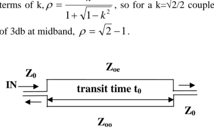
Directional couplers date back to a patent filed in 1922 [4] and were then called “transposed loop antennas”. Most of the basic work was completed by the 1960s [5]; Cohn and Levy summarized the history in an excellent 1984 review article [6]. There is of course a parallel literature on crosstalk, which deals with the same coupled line equations but it also covers weak coupling approximations, multiple lines, dielectric inhomogeneity, and impedance mismatches [7]. The two-line directional coupler, ideal in theory and near-ideal in manufacture, is our interest here. It has velocity-matched even and odd modes that solve the coupled line equations, and overall impedance matching to a system impedance of Z0, as described in
the above references.
Coupled line theory [5,8] gives the induced voltage on Line 2 (Figure 1) as
(1)
and θ=ωπ/(2ω0), ω0 the ¼ wave frequency. Zoo and
Zoe are the odd and even mode impedances. In Fig. 1,
,
oo oeoo oe
Z
Z
Z
Z
k
+
−
=
.
sin
cos
1
sin
2 12
θ
θ
θ
j
k
jk
V
V
+
−
all four ports are presumed to be impedance matched, most often to 50 ohms. A pulse on Line 1, left to right, is coupled to Line 2, with the coupled signal traveling right to left. The condition
Z
0=
Z
oeZ
oo means that capacitive and inductive coupling are balanced such that they add for the coupled signal on the lower left, Line 2 (coupled port), and cancel on the right of Line 2 (isolated port), as shown.Figure 1. Coupled lines; all 4 ports are presumed to be Z-matched. A pulse on Line 1, left to right, is coupled to Line 2. If capacitive and inductive coupling are properly balanced, the coupled signal emerges on the lower left, Line 2 (coupled port), and is cancelled on the right of Line 2 (isolated port).
The induced voltage equation, Eq. 1, above, shows that a strongly-coupled directional coupler of the proper quarter wave frequency would nearly differentiate the rising edge of a (slow enough) TLP pulse, as the differentiation is nearly perfect in the small-angle approximation for low frequency. If the falling edge of that TLP pulse is very slow, as will be described later, there is substantially no second pulse. This offers intriguing possibilities for CDM-like pulses.
Throughout its history, most of the analysis of the directional coupler, as well as its use, has been in the frequency domain. While the crosstalk literature is more agreeable to examining the time domain response, usually other conditions (e.g., multiple lines, impedance or mode mismatch, low phase shift, weak coupling, etc.) apply. Thus we had to use computer simulation to find such things as the step response of two rather strongly coupled lines in a directional coupler.
B. Computer Simulation of Step
Response
Computer simulation of the coupled-line system was used to provide further insights into the time domain response of directional couplers, and aid design
decisions. The authors studied the response of the coupler to the following input rising edge waveforms, shown in Figure 2, describing a step:
2 1 ) ( 812 . 1 2
1 − 0 +
=
r input
t t t erf
v (2), and
2 1 ) )( 4 . 0 tan 2 ( arctan
1 − 0 +
=
r input
t
t t
v
π
π
(3),Cm Lm
Line 1
Line 2
Cm Lm
Line 1
Line 2
where tr is the 10%-to-90% rise time of the input
voltage waveform and t0 the center position. These
equations are chosen because they describe step functions with finite rise time and their derivatives are the Gaussian and the Lorentzian functions, respectively, the shapes of which resemble measured waveforms of CDM pulses. For the moment we do not examine step functions with some overshoot of the final voltage, which would be useful in approximating standard CDM waveforms because of the undershoot [9,10], but we will return to that point later.
Error Function/Arctangent Step with 1ns Rise Time
-0.1 0.1 0.3 0.5 0.7 0.9 1.1
0 0.5 1 1.5 2 2.5 3 3.5 4 Tim e [nSec]
V
o
lt
ag
e [
V
]
Error Function Arctangent
Figure 2. Plot of step function using error function or arctangent, as in Eqs. 2 and 3, and used in coupler simulations. One nanosecond is the 10-90% rise time in each case.
658
.
0
,,
≈
input r
coupled r
t
t
. (4)
This number is driven by the 10%-to-90% definition of rise time; for a rise time definition of limits arbitrarily close to 0-to-100%, the ratio approaches the more familiar √2/2 or 0.707….
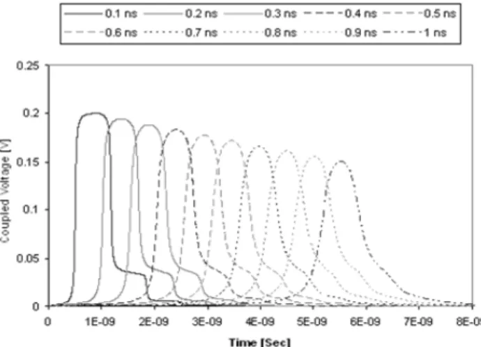
Figure 3. Coupled voltage waveforms of directional coupler with 1V error function input waveforms, resulting in 0.5V traveling waves on the input. The quarter-wave frequency of the coupler is 750MHz, time-of-flight (2t0) is 667 psec.
Figure 4. Coupled voltage waveforms of directional coupler with 1V arctangent input waveforms and other conditions as in Fig. 3.
As the rise time reduces much below the time-of-flight of the coupler, another limiting case emerges. The rise time of the coupled pulse approximately equals that of the input pulse, and it becomes much like a short, square TLP pulse yet still nicely z-matched. As the coupling to the victim line does not settle until the input excitation reaches the far side of the attacker line, the coupled waveform is broad and flat compared to the derivative of the input voltage,
and has a width equal to the round trip time-of-flight. Figure 3 shows families of Gaussian output waveforms in response to inputs of various rise times for a coupler having f0=750 MHz and 3db (k=0.707)
coupling at f0. Lorentzian waveforms are similar but
converge to the derivative more slowly due to the sharpness of the Lorentzian function, as shown in Figure 4. Figure 5 shows the full relationship for the error function input and Gaussian coupled waveforms, including the asymptote of Equation (4). This slope of less than 1 actually helps to stabilize the rise time. As expected, Figs. 3-4 show that the differentiation is more accurate with longer rise times (or, equivalently, shorter coupled line length), but the amplitude of the coupled voltage also declines at longer rise times. Thus the designer of the CDM-TLP apparatus must consider the proper trade-off between differentiator behavior and output pulse magnitude. Nonetheless, the Gaussian pulse (Fig. 3) is fairly accurate for error function rise times above or even slightly below the time-of-flight of the coupler, without much loss in amplitude. Also, note in Fig. 3 how slowly the pulse width varies over a wide range of input rise times. This is because the coupled charge packet is constant, fixed by the coupler properties and the input’s final voltage (see Appendix A). For the 750 MHz 3 db coupler, for example, k=0.707 and the charge packet is 6.67 pC/V. With the charge packet and pulse rise time driven far more by the coupler design than the switch arc, more uniform response of devices is expected.
0 0.5 1 1.5 2 2.5 3
0 0.5 1 1.5 2 2.5 3 3.5
Ris e Tim e of Input V oltage [ns e c]
R
is
e
Ti
m
e
of
Cou
p
le
d
V
o
lt
a
g
e
[
n
s
e
c
]
4 y = x
y = 0.658x
Figure 5. Rise times of input and coupled voltages with error function excitation. The two rise times are the same at low rise times and have a ratio of 0.658 at high rise times.
III. Pulse Formation Hardware
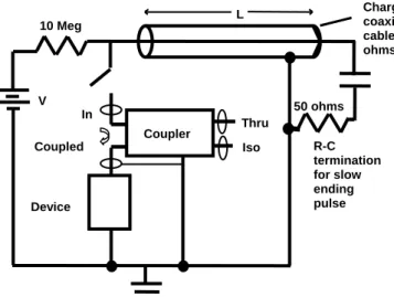
step function that first goes into a 4-port directional coupler, Z-matched on its thru and isolated ports, and the signal from the coupled port goes to the device. This signal approximates the derivative of the TLP pulse’s rising edge, as has been discussed, and thus is very short, on the order of nanoseconds. Ideally, we would like the basic transmission line pulse to have a sharp rising (or initial) edge, but no falling (or trailing) edge to speak of, since we want a single CDM-like pulse from the coupler, not two. This is achieved in a regular TLP system as shown in Fig. 6 by adding an RC termination to the opposite end of the line, as shown. With a line impedance as the resistor (usually 50 ohms) and a substantial capacitance standing off the charging voltage, the z-match looking back into the line is nearly perfect, and the resulting TLP pulse at the front end has a very gradual trailing edge, with no substantial “echo” pulse out of the coupler. In addition, reflected pulses from an unmatched target (the DUT) disappear into the charged line and into the thru line match, with theoretically perfect z-matching. We have measured the return loss of this matching to be better than 24 db even when the coupled pulse is completely reflected back into the coupler.
Figure 6. 50-ohm TLP system converted to CDM-TLP, by use of RC termination (absorbs reflected pulse from device and coupler) and 3db hybrid coupler [11]. The latter produces a fast, short pulse on the transmission line into the device. Thru and isolated ports of the coupler are terminated by 50 ohms.
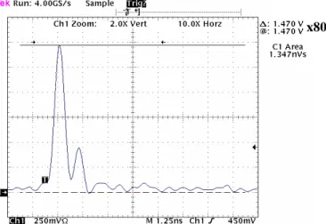
The coupled pulse is one for which Figure 7 is a good example, one very much resembling the CDM waveform pictured in standards from the ESD Association and JEDEC [9,10]. The charge packet in Fig. 7 is a rather extreme example, but shows how large and fast, and CDM-like, those pulses can be when taken to the limits of the equipment. Figure 7 was a pulse produced by a 7kV charge on the line (in a NoiseKen INS-4001 TLP system) and a 3.5kV
traveling wave into a 750 MHz nominal 3db coupler (we estimate k=0.759, but it is customary for commercial couplers to have k>0.707 so that 3db or better is achieved over a substantial bandwidth). The 39 nC of the initial spike is then followed by about 12 nC of undershoot, so the net charge is 27 nC. This is almost exactly what the Total Charge Theorem (Appendix A) predicts (27.2 nC, or 7.77 pC/V). If the target were a reflecting short instead of a 50-ohm match, then of course the absorbed charge and peak current would be doubled.
Figure 7. Setup resembling Fig. 6 used with 3.5kV wave on 50 ohm TLP to produce 39 amps and 39 nC, before the undershoot, into 50 ohms. With a highly reflecting target device, nearly 2X that amount of current and charge would result. A nominal 3db
hybrid Lange coupler with f0=750 MHz was used; rise time is
fairly stable near the time of flight, 2t0=667 psec. Pulse
measurement was on the Tek 784D oscilloscope with an 80x probe.
It is very likely that the undershoot in Fig. 7 was caused by some overshoot in the TLP pulse, created by the system in Fig. 6. It is clear that a little capacitance at the left-hand end of the charged cable in Fig. 6 could allow for that overshoot in the step function pulse. A familiar laboratory method for doing this in a tunable way is to twist two short pieces of insulated wire together to form a parallel open stub of variable electrical length.
The coupler itself is a conventional quarter-wave directional coupler, designed for strong coupling (3db or less) and high voltage tolerance, in order to produce a strong signal. Off-the-shelf 3db stripline Lange couplers [12] could be used were it not for the desired high voltage tolerance of several kilovolts. We eventually settled on a custom commercial high-voltage Lange coupler design, used for the waveforms in Figures 7 and 8, the aforementioned 750 MHz 3 db coupler. At present it is used in conjunction with a hardware setup as in Fig. 6, assembled in our lab from Coupled
Thru L
V 10 Meg
Iso Coupler
In
Device
R-C termination for slow ending pulse
Charged coaxial cable, 50 ohms
50 ohms
inexpensive parts. Figure 8 shows the result of a step of moderate voltage (277V) going through the coupler to produce a very fast pulse with 2.35A peak current into a 50 ohm load. The integrated 2.15 nC is in excellent agreement with the Total Charge Theorem, Appendix A, as we discussed earlier how the expected charge is 7.77 pC/V. The secondary pulse of Fig. 8 is partly due to ringing in the rising edge of the step, which can be corrected. Any contribution from second time-step effects, as indicated in Eq. A2 of the appendix, can be much reduced by using a weaker coupler, also indicated by Eq. A2, as long as the pulse is still acceptably strong.
Figure 8. Same coupler as in Fig. 7, used at lab-built TLP system to produce this CDM-TLP waveform into 50 ohms from a 277V step input. Tek 784D and 80x voltage probe were used, so the peak current is about 2.35A. The area is also multiplied by 1.6 to give nC of total charge.
At the beginning of this work, we proved all the basic concepts using a novel class of high voltage couplers as in Figure 9, since the commercial high-voltage couplers, acquired later, required extra lead time and expense. These coaxial couplers are simple to build at an ordinary electronics lab bench, and are a variant of the re-entrant coaxial coupler [13] as discussed in another context in some of the authors’ more recent work [14]. Fig. 9 resembles Cohn’s re-entrant coaxial coupler except that the inner shield and return ground are turned inside out, such that the common shield becomes coupled to free space as well, but only for the even mode [11]. For the odd mode, the shield and ground are part of the electric wall [13]. Accordingly, there could be a velocity mismatch between even and odd modes, but for the arrangement shown in Fig. 9 we achieved a reasonable balance by choosing a slower cable for the return ground, which participates in even mode only. We wanted that to average favorably with the even mode fields in air from the floating shield, although the latter has a thin dielectric
around it because it should be insulated for safety reasons. The result was reasonable directivity, as the signal on the isolated port was then 14-16 db down from the coupled port signal, certainly good enough to avoid wasting coupled energy. While the odd mode impedance Zoo is easily calculated from the cable
impedances in Fig. 9 as 19.3 ohms [13,14], the even mode is again influenced by the free space fields, without which the system impedance would be 57 ohms and Zoe would be 169.3 ohms. However, the
impedance match turned out to be pretty good due to the free space coupling in parallel, maybe 51 or 52 ohms, and a coupler about 12 cm long was measured at low frequency (Eq. 1 in section IIA, above) to have k=0.809, with an expected f0 of 500 MHz. This
results in an expected 13.76 pC/V of charge in response to a step.
Figure 9. Coaxial cable coupler; cross-sectional view at either end. See also Fig. 1 and [13,14]. Shields all float. Length of
cables is chosen for proper quarter wavelength frequency ω0.
Coaxial cable tolerates very high voltage. 52 cable: Belden 9311, 75% velocity, 52 ohms; 75F cable: Belden 9259, 78% velocity, 75 ohms; 75S cable: Belden 8241, 66% velocity, 75 ohms
Isolated
port
Thru port
Gnd return
50 ohm
52 52
75S
75F 52
50 ohm
52 75F
Input port
Gnd return
52 52
Coupled
port
75F
52 52
75F
75S
Figure 10. CDM-TLP waveform resulting from coaxial coupler as in Fig. 9, 273V step applied to input; same measurement system as earlier. Peak current of 2.16 A might be a little lower than calculated due to slight mismatches in this lab-built coupler.
Figure 10 is a waveform resulting from a 273V input step into the coaxial coupler of Fig. 9, again with an 80x probe and a 50 ohm match. The measured 3.73 nC of charge compares well to the predicted 3.76 nC from the Total Charge Theorem using the above deduction of k=0.809 from measurements at 20-50 MHz (notice that measurement of coupled voltage at low frequency, Eq. 1, combines k and t0 in the same
way as Eq. A4). The rise time is still fast, and the pulse is a bit wider because the time step is now 1 nsec instead of 667 psec. But like the other pulses, it is essentially over by 2.5 nsec, very much like a CDM pulse.
IV. Conclusion
We have shown that some simple components, a directional coupler and an RC termination, can be added to an ordinary TLP system to produce short CDM-like pulses on a transmission line. The coupler and the entire pulse-formation system are impedance-matched and will absorb any reflections from an unmatched load. A strong (3 db or less) high voltage quarter-wave directional coupler can be used to form short, sharp pulses resembling CDM and containing many nanocoulombs of charge. Weaker directional couplers can also be used, and produce fewer trailing echoes for an even sharper pulse, but the charge per volt will be lower.
We have presented a Total Charge Theorem for directional couplers and impedance-matched coupled pairs of lines that accurately predicts the total charge in the coupled line that results from a voltage step on the input. It is a function only of the voltage step height, the coupling constant and electrical length of the coupler, and the system impedance. Thus a charge packet of fixed size can be expected from a given TLP
voltage step, regardless of exact waveform. This means that a charge packet from a voltage step modified by a rise time filter will be unaffected, except by the dc insertion loss of the filter. The Total Charge Theorem is a general property of directional couplers and comes from consideration of the time domain instead of the frequency domain, much like certain crosstalk formulations of coupled lines but with particular attention to step response. We feel that the Total Charge Theorem has wider application than the present CDM-TLP work because impedance-matched directional couplers are now being used in such applications as high-speed digital multi-drop memory busses [15, 16]. The Total Charge Theorem applies strongly to these signals and provides a useful tool for understanding of them.
x80
The coupler produces pulses with a time scale set by the electrical length of the coupled section. It can be arranged to approximately differentiate the rising edge of a TLP pulse to produce CDM-like pulses with remarkably stable rise time, pulse width and total charge. From an error function step waveform, for example, a near-perfect Gaussian pulse can be realized without much loss of ideal maximum amplitude from the coupler. These CDM-like pulses should be useful in further studies of CDM phenomena and in CDM testing of devices.
Appendix A: Total Charge Theorem
for directional couplers and Z-matched
coupled lines
Consider a two-line directional coupler with system impedance Z0 and the impedance-matched condition
oo oeZ
Z
Z0 = , where Zoe and Zoo are the even and odd
mode impedances respectively. Under these conditions, the even and odd modes and their reflection coefficients are complementary, so that at all frequencies the input port is impedance matched (no reflection because reflected even and odd modes cancel) and the isolated port is null. Thus a single reflection coefficient
oo oo
oe oe
Z Z
Z Z Z Z
Z Z
+ − = + − =
0 0
0 0
ρ
is sufficient to describe the response to an abrupt traveling wave voltage step ∆V at the input port, as that step can be decomposed into equal parts even and odd mode signals, and the mode reflection coefficients with respect to Z0 are of opposite sign.
terms of k, 2
1
1
k
k
−
+
=
ρ
, so for a k=√2/2 couplerof 3db at midband,
ρ
=
2
−
1
.Figure A1. Directional coupler impedance scheme, with input and coupled ports on the left, thru and isolated ports on the right.
When
Z
0=
Z
oeZ
oo , isolated port (lower right of Fig. 1) isnull.
Figure A1 sketches the mode impedance as it splits into complementary even and odd modes over the length of the coupler and then becomes Z0 again
beyond the coupled lines. The reflection and transmission coefficients at the two interfaces determine the response for each time step. The response at the coupled port to an abrupt voltage step
∆V at the input port is an infinite series of timed steps, starting with V1=ρ∆V for the first time step and then
reduced at each succeeding time step by an amount due to transmission and reflection at the two interfaces with Z0 impedance. It takes one “time step”
to sense the abrupt transition back to Z0 at the far end
of the coupler, so a time step is the round trip propagation time for the coupled line section; let this time be 2t0.
Understanding that the odd mode is wholly complementary to the even mode, let us focus on the even mode to solve for the wave series. For the even mode, the reflection coefficients at the left and right interfaces in Fig. A1 are ρ and -ρ, respectively, while the transmission coefficients for right-going and left-going waves at the left-hand interface are
ρ
τ
=
+
+
=
2
1
0 1 oe oe
Z
Z
Z
and
τ
=
−
ρ
+
=
2
1
0 0 2 oe
Z
Z
Z
, respectively.After one time step the coupled port has an additional term -τ1τ2ρ∆V, due to the first reflection at the
right-hand interface, reducing the total voltage. Each succeeding time step has an additional term like the above but with an additional factor of ρ2, due to two more interfacial reflections. Thus the general
expression for the coupled voltage during the nth time step is )), ... 1 )( 1 ( 1 ( )) ... 1 ( 1 ( 4 2 4 2 2 4 2 4 2 2 1 − − + + + + − − ∆ = + + + + − ∆ = n n n V V V
ρ
ρ
ρ
ρ
ρ
ρ
ρ
ρ
τ
τ
ρ
Z
oefor n≥2. (A1)
The truncated series can be captured using standard methods so that
1 2 2 2 2 2
)
)
1
(
)
1
)(
1
(
1
(
− −∆
=
−
−
−
−
∆
=
n nn
V
V
V
ρ
ρ
ρ
ρ
ρ
,for n≥1. (A2)
Now that we have the voltage time series, the current can be found for each time step and summed to give total charge 0 0 4 2
2
...)
1
(
t
Z
V
Q
=
ρ
∆
+
ρ
+
ρ
+
0 0
2
2
)
1
(
Z
t
V
ρ
ρ
−
∆
=
. (A3)This is also 0
0 2
1
t
Z
k
V
k
Q
−
∆
=
. (A4)It is clear that Eqs. A3-A4 apply to the net charge coupled by a net voltage step ∆V of arbitrary form, i.e.,
∆
V
=
V
(
t
)
−
V
(
0
).
Any signal resulting in a net change ∆V can be broken down into a set of infinitesimally small abrupt steps, each of which has the multiplier of Eqs. A3-A4. All of these terms then sum to the same net effect as expressed in Eqs. A3-A4.Acknowledgments
The authors wish to thank Tina Cantarero for the hardware construction, many of the lab measurements, and for manuscript preparation. We also thank Mohsen Alavi, Babak Sabi and Chuck Korstad for managerial support, and John Benham for manuscript review.
References
[1] T. Maloney and N. Khurana, "Transmission Line Pulsing Techniques for Circuit Modeling of ESD Phenomena", EOS/ESD Symposium Proceedings, 1985, pp. 49-54.
Z
0IN
transit time t
0
[2] H. Gieser, M. Haunschild, “Very-Fast Transmission Line Pulsing of Integrated Structures and the Charged Device Model”, EOS/ESD Symposium Proceedings, 1996, pp. 85-94.
[3] H. Wolf, et al., “Capacitively Coupled Transmission Line Pulsing CC-TLP—A Traceable and Reproducible Stress Method in the CDM Domain”, EOS/ESD Symposium Proceedings, 2003, pp. 338-345.
[4] H.A. Affel, “High Frequency Signaling System”, US Patent 1,615,896, filed Dec. 15, 1922; issued Feb. 1, 1927.
[5] G. Matthaei, L. Young, and E.M.T. Jones, Microwave Filters, Impedance-Matching Networks, and Coupling Structures (New York: McGraw-Hill, 1964; reprinted by Artech House, 1980), pp. 798-800.
[6] S.B. Cohn and R. Levy, “History of Microwave Passive Components with Particular Attention to Directional Couplers”, IEEE Trans. Microwave Theory and Techniques, vol. MTT-32, pp. 1046-1054, Sept. 1984.
[7] S.J. Orfanidis, Electromagnetic Waves and Antennas, Ch. 10 (2004), posted at http://www.ece.rutgers.edu/~orfanidi/ewa.
[8] D.M. Pozar, Microwave Engineering (New York: J. Wiley and Sons, 1998).
[9] ESD Association test standard 5.3.1, “Charged Device Model (CDM)—Component Level”, 1999. See www.esda.org.
[10] JEDEC JESD22-C101-A standard, “Field-Induced CDM Test Method”, June 2000. See www.jedec.org.
[11] Timothy J. Maloney, "Pulse Coupling Apparatus, Systems, and Methods", US Patent Application, filed by Intel June 26, 2003.
[12] J. Lange, “Interdigitated Stripline Quadrature Hybrid”, IEEE Trans Microwave Theory and Techniques, MTT-17, pp. 1150-51, Dec. 1969. [13] S.B. Cohn, “The Re-Entrant Cross Section and
Wide-Band 3-db Hybrid Couplers”, IEEE Trans. Microwave Theory and Techniques, vol. MTT-11, pp. 254-258, July 1963.
[14] T.J. Maloney, D.-H. Cho, S.S. Poon and B. Lisenker, "Improving the Balanced Coaxial Differential Probe for High-Voltage Pulse Measurements", 2001 EOS/ESD Symposium Proceedings, pp. 398-407.
[15] John R. Benham, et al., “An Alignment Insensitive Separable Electromagnetic Coupler for High-Speed Digital Multidrop Bus Applications”, IEEE Trans. Microwave Theory and Techniques, vol. MTT-51, pp. 2597-2603, Dec. 2003.