Laanait et al. Adv Struct Chem Imag (2017) 3:11
DOI 10.1186/s40679-017-0044-3
RESEARCH
Dynamic X-ray diffraction imaging of the
ferroelectric response in bismuth ferrite
Nouamane Laanait
1,2*, Wittawat Saenrang
3, Hua Zhou
4, Chang‑Beom Eom
3and Zhan Zhang
4Abstract
X‑ray diffraction imaging is rapidly emerging as a powerful technique by which one can capture the local structure of crystalline materials at the nano‑ and meso‑scale. Here, we present investigations of the dynamic structure of epitaxial monodomain BiFeO3 thin‑films using a novel full‑field Bragg diffraction imaging modality. By taking advan‑ tage of the depth penetration of hard X‑rays and their exquisite sensitivity to the atomic structure, we imaged in situ and in operando, the electric field‑driven structural responses of buried BiFeO3 epitaxial thin‑films in micro‑capacitor devices, with sub‑100 nm lateral resolution. These imaging investigations were carried out at acquisition frame rates that reached up to 20 Hz and data transfer rates of 40 MB/s, while accessing diffraction contrast that is sensitive to the entire three‑dimensional unit cell configuration. We mined these large datasets for material responses by employing matrix decomposition techniques, such as independent component analysis. We found that this statistical approach allows the extraction of the salient physical properties of the ferroelectric response of the material, such as coercive fields and transient spatiotemporal modulations in their piezoelectric response, and also facilitates their decoupling from extrinsic sources that are instrument specific.
© The Author(s) 2017. This article is distributed under the terms of the Creative Commons Attribution 4.0 International License (http://creativecommons.org/licenses/by/4.0/), which permits unrestricted use, distribution, and reproduction in any medium, provided you give appropriate credit to the original author(s) and the source, provide a link to the Creative Commons license, and indicate if changes were made.
Background
Capturing the evolving structure of materials in func-tional devices under a host of varying thermodynamic potentials and environments, with nanoscale resolutions and in real-time, remains of one of the most actively pursued goals of structural imaging [1]. Out of the exist-ing structural probes, X-ray diffraction-based micros-copy enjoys a host of properties that are ideally suited to achieve the aforementioned goal: namely, the depth pen-etration of hard X-rays, their exquisite sensitivity to the atomic structure, and analytical power facilitated by their weak interactions with matter [2].
In contrast to well-developed structural probes such as dark field transmission electron microscopy [3], X-ray diffraction microscopy has been traditionally hampered by the availability of optics that can simultaneously oper-ate in the hard X-ray regime and provide large numeri-cal apertures for nanosnumeri-cale resolution. Fortunately, the combination of continued advances in X-ray optics [4],
the ever-increasing brightness of synchrotron sources [5], and sophisticated phase-retrieval algorithms has spurred a resurgence in X-ray diffraction-based imaging and has led to a diverse set of imaging modalities [6]. Of particu-lar interest are those X-ray imaging modalities that place no restriction on the sample size nor its geometry and are of applicability to materials in thin-film form; one of the most technologically important class of materials. These modalities consist of: (i) nano- and micro-diffraction probes, whereby a focused beam is rastered across the sample to spatially map the diffracted intensity across a sample [7–9]; (ii) Bragg ptychography, where a real space image is reconstructed out of overlapping nano-diffrac-tion patterns using phase-retrieval algorithms [10, 11]; (iii) full-field dark field X-ray microscopes which employ a combination of hard X-ray optics to form a real space image of the sample with diffraction contrast [12, 13].
Full-field dark field X-ray microscopes represent a novel extension of the widely used transmission X-ray microscopes, from an absorption-based contrast to dif-fraction contrast. These microscopes have been used to probe the static and dynamic structure of crystal surfaces [14, 15], reconstruct the three-dimensional crystal grain
Open Access
*Correspondence: [email protected]
1 Center for Nanophase Materials Sciences, Oak Ridge National
Laboratory, Oak Ridge, TN 37831, USA
orientations in metals [13], and capture lattice rotations near misfit dislocation networks in complex oxide thin-films [16]. The highest spatial resolution that has been achieved in a full-field dark field X-ray microscope (sub-100 nm) [12] is coarser than that of both nano-diffraction probes (~few tens of nanometers) and Bragg ptychography (sub-10 nm), yet its temporal resolution is orders of mag-nitudes finer, with image acquisition times as short as few tens of milliseconds. As we show here, this combination of nanoscale resolution and high-frame rates enables full-field X-ray diffraction microscopes to probe the structural changes of crystalline materials in situ and in operando.
In this article, we demonstrate for the first time the capability to investigate the electric field-driven dynamic structural responses of buried monodomain bismuth fer-rite epitaxial thin-films [17] in micro-capacitor devices at unprecedented spatiotemporal resolutions. By employing a full-field Bragg X-ray diffraction microscope (XDM), we demonstrate that a real space image with a field of view of ~15 × 15 μm2 and ~70 nm lateral spatial
reso-lution is captured with an acquisition time as small as 50 ms. These imaging characteristics make XDM one of the most data-intensive, high-throughput synchro-tron-based techniques, whose frame rates reach up to 20 Hz, and since each frame (i.e., a full image) contains 1024 × 1024 pixels (16-bit depth), its data transfer rates from the detector are as high as ~40 MB/s. By using a combination of diffraction contrast mechanisms, we probed the dynamically induced ferroelectric polariza-tion and piezoelectric responses in bismuth ferrite as a function of electric field. To extract material responses from the large XDM datasets, composed of 102–103
images, we use matrix decomposition techniques such as independent component analysis. We found that this sta-tistical-based approach allows the extraction of key mate-rial responses such as polarization coercive fields as well as transient spatiotemporal piezoelectric responses due to the onset of device fatigue. Furthermore, we find that matrix decomposition techniques also facilitating decou-pling of the measured material responses from extrinsic sources present in the data that are instrument specific.
Methods
Sample and device preparation
Monodomain epitaxial BiFeO3 thin-films (400 nm) were
grown by off-axis sputtering on a vicinal substrate of SrTiO3 (001) [18], with a metallic bottom electrode of
SrRuO3 (30 nm) [19]. The miscut direction of the
sub-strate is parallel to SrTiO3 [110] with the miscut angle of
4o. An array of micro-electrodes of Pt (~100 nm thick)
were fabricated on the surface of the sample by photoli-thography (see Fig. 1a).
The samples were mounted on standard microchip carriers. Electrical grounding of the samples was per-formed by contacting the SrRuO3 bottom electrode,
that is exposed from the side of the sample, with one of the terminals of the carrier using conductive silver paste. Wire-bonding with aluminum was used to con-nect different Pt electrode pads to the lead terminals of the chip carrier. In this micro-capacitor configuration, the BiFeO3 devices recorded resistances on the order
of ~100 MΩ and large ferroelectric polarization values of ~70 μC cm−2. The electrical poling studies were
per-formed using an arbitrary waveform generator (Tektro-nix) connected to a piezoelectric DC driver to provide well-defined voltage pulses.
Reciprocal space mapping
Structural characterization of the samples was per-formed using synchrotron hard X-ray reciprocal space maps (RSM) at the Advanced Photon Source (33 BM-B) with an X-ray energy of 15.5 keV. Reciprocal space vol-umes near SrTiO3 (STO) 002 and 103 Bragg reflections
were reconstructed from diffraction patterns by an area-based detector (Pilatus, Dectrix) acquired during angular scans of the Bragg angle at different angular inclinations of the sample with respect to the surface normal [20]. An HL-cut of the reciprocal space volume near STO 002 is shown in Fig. 1c. The large spread of the BiFeO3 (BFO)
002 reflection indicates the presence of substantial crys-tal mosaicity. These different mosaic block configurations are directly imaged in real space by X-ray diffraction microscopy (see below).
BiFeO3 is a well-known multiferroic, hosting both
anti-ferromagnetism and ferroelectricity [21]. The crystal structure of BiFeO3 is rhombohedral with space group R3¯c, where the polarization vector P points along ⟨111⟩
Page 3 of 12 Laanait et al. Adv Struct Chem Imag (2017) 3:11
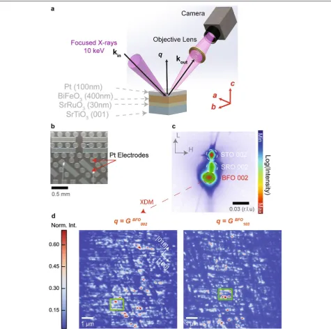
Fig. 1 X‑ray diffraction imaging of buried ferroelectric domains in a micro‑capacitor configuration. a Schematic of the X‑ray diffraction microscope (XDM), the scattering geometry, and characteristics of the sample (not drawn to scale). The imaging contrast of XDM is determined by the scatter‑ ing vector, q=kout−kin, where k (|k| =2π/) is the wavevector of the X‑ray wavefield (≈1.2 Å). A side view of the device indicates the thick‑
ness of the metallic electrodes [top Pt, bottom SrRuO3 (SRO)], and the ferroelectric thin‑film BiFeO3 (BFO) that was grown on single crystal SrTiO3
(001). b Optical image of the device showing the Pt electrode patterning (top view). c Reciprocal space map (RSM) near STO 002 Bragg reflection. All reciprocal space coordinates are expressed in terms of SrTiO3 reciprocal lattice units (r.l.u). The BFO 002 Bragg reflection is offset in the HK‑plane
with respect to STO due to growth on a substrate with a high miscut angle (~4°, direction along STO [110]). d XDM images taken at different Bragg reflections of BFO (left: 002, right: 103). Spatial variations in the diffracted intensities are due to the presence of considerable lattice rotations (mosaicity) and epitaxial strain relaxation due to the large thickness of the film. Boxes in the images outline different mosaic blocks. The similarity in diffraction contrast between XDM images at G002 and G103 provide direct evidence for the mono‑domain configuration of the ferroelectric thin‑film
samples has an out-of-plane component that is parallel to [001] and in-plane component that is parallel to [ ¯110]¯ . We verified the mono-domain property of the BFO sam-ples by RSM of BFO 103 and 113 reflections, showing no reflection peak splitting associated with a multi-domain configuration (Additional file 1: Figure S1) [24].
X‑ray diffraction microscopy
Structural imaging of the samples was performed at the Advanced Photon Source (XRIM instrument, 33ID-D). X-ray diffraction microscopy is a full-field imaging tech-nique with an optical configuration that is composed of: (1) a condenser lens to illuminate the sample; (2) objec-tive lens to form an image out of the Bragg diffracted wavefield. The condenser lens is composed of a pair of dynamically bendable Kirkpatrick–Baez mirrors that focus the X-ray beam (10 keV, 15 × 15 μm2) on the
sam-ple surface. The objective lens is a Fresnel zone plate (FZP) with 60 nm outermost zone width, that pro-jects the image onto a sCMOS camera with a pixel size of 6.5 μm (Neo 5.5, Andor) that can be operated up to 100 frames per second (i.e., 100 Hz). The sCMOS cam-era is coupled to a scintillator for conversion from X-ray to optical, in addition to an oil-immersion lens (Nikon) for 20× optical magnification. The total magnification of XDM (~440×) is the product of FZP magnification (~22) and optical magnification, producing an effective pixel size of 15 nm on the sample and a field of view of ~15 × 15 μm2. The lateral resolution of XDM is ideally
60 nm and limited by the outermost zone width of the FZP. However, due to persistent mechanical vibrations in the instrument, the lateral resolution has been previously determined at ~70 nm. Additional experimental details on XDM have been reported elsewhere [12].
In this current configuration, XDM can acquire real space images of crystalline thin-films with Bragg diffraction intensities of thin-films on the order of 10−5 × I
o with signal-to-noise ratios of 10:1 in 1 s, where Io ∼1012 photons/s is the incident flux on the sample.
Due to the scaling of thin-film diffraction as N2, where N is the number of coherently scattering thin-film lay-ers, thicker films inherently lead to stronger signals and images with field of view and lateral resolution specified above can be acquired in 10s of milliseconds (see below).
The contrast in XDM images is determined entirely by the scattering vector qHKL, where HKL are the Miller
indices (see Fig. 1a). Representative images of BFO acquired at the 002 and 103 Bragg reflections are shown in Fig. 1d, with q=G002 and q=G103, respectively. For every image pixel (x,y) is associated a diffracted inten-sity, Iq (x,y), from a region of the film whose real space location on the sample surface is (x,y). Due to the depth penetration of 10-keV X-rays (~microns), an XDM image
contains information that is sensitive to the full three-dimensional spatial distribution of (HKL) planes, with a lateral spatial resolution that is on the order of ~70 nm (5 × pixels) but with imaging contrast that is diffrac-tion limited (resoludiffrac-tion ~ dHKL/2). Both XDM images in Fig. 1d show the presence of mosaic blocks on the order of a micron (outlined in Fig. 1d). The intensity variations across the images originate from (002) and (103) lattice plane rotations introduced by various epitaxial strain relaxation mechanisms, which moves their scattering out of the Bragg condition. The spatial variations in these lat-tice rotations from one mosaic block to another can be directly extracted from XDM images [16]. Furthermore, note that the similarity in XDM image contrast between the 002 and 103 reflections is further confirmation that the BFO samples are indeed in a mono-domain config-uration, since splitting of the 103 reflection by multiple domain variants would substantially modify the XDM contrast, leading to the appearance in XDM images of real space ferroelastic domain patterns along preferred crystallographic orientations, to satisfy mechanical com-patibility conditions of BiFeO3 [25] (e.g., see [12] for
XDM imaging of ferroelastic domain walls).
Results
Imaging of the out‑of‑plane ferroelectric response
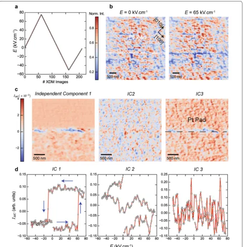
Taking advantage of the depth penetration of hard X-rays, we acquired images of the changes in the local structure of BFO buried underneath the 100 nm Pt pads during electrical poling. The electric field E was applied between Pt and SRO and is oriented along the c-axis of the sample. A full poling cycle was performed (Fig. 2a), during which an XDM image was acquired at each value of E.
Ferroelectric materials such as BFO also exhibit a con-verse piezoelectric effect, whereby an applied electric field leads to expansion/contraction of the material [26]. This change in the material causes a shift in the scat-tering angle (2θ) at a Bragg reflection (e.g., 002) and is one method by which to achieve imaging contrast (see below). Here, we suppressed XDM contrast sensitivity to the converse piezoelectric by offsetting the scattering vector to q0,0,2−δ, with δ ≈ 10−1. XDM images taken at
this scattering condition under zero field and 65 kV cm−1
Page 5 of 12 Laanait et al. Adv Struct Chem Imag (2017) 3:11
Fig. 2 Imaging the ferroelectric switching of BiFeO3. a The poling cycle applied in the presented XDM dataset, where E is the electric field between
the Pt and SRO electrodes and is oriented along [001]. At each point an electric pulse lasting 0.5 s is applied, followed by acquisition of an XDM image (acquisition time 0.2 s) with q0,0,2−δ, where δ≈ 10−1. b Representative XDM images taken at different values of the electric field cycle in a.
The dashed line in the right panel indicates the edge of the Pt electrodes. After poling the BFO film underneath the Pt electrode, the domain‑wall between two regions of the film with opposite out‑of‑plane polarization vectors produces amplitude contrast (negative) in diffraction imaging. The entire collection of XDM images acquired during the electric field cycle (~200 images) are unmixed using independent component analysis (ICA), assuming three independent components or sources. In c the XDM collection is projected onto these three different basis vectors and reshaped into images, while d shows the corresponding evolution of these independent components (IC) as a function of electric field. The landmark hyster‑ esis polarization loop of BFO is obtained directly from IC1 and its spatial map in c shows the domain wall between the two opposite polarization states. The arrows in d indicate the direction of the poling cycle. The other two ICA components IC2, three are mostly closely associated with extrin‑ sic instrumental factors that enter the data such as X‑ray beam intensity fluctuations or drift, given that their evolution during the poling cycle is not physically relatable to ferroelectric behavior. IMC represents the mean‑centered intensity, whereby the mean intensity in each image in the original
the polarization direction changes). The offset from the Bragg condition, δ≈10−1
, was empirically tuned to max-imize intensity contrast for the domain wall, but could be determined, in principle, from a full analysis of diffrac-tion contrast as well as optical responses of XDM.
To extract the fundamental properties of the system’s ferroelectric response from the XDM images, the field-driven changes in image contrast must be analyzed. Note that over the course of a single poling cycle, more than 200 images were acquired at increments of 1.25 kV cm−1;
such a fine resolution is needed given the abrupt change in polarization. To mine such large data sets in an unsu-pervised and statistically rigorous manner we used inde-pendent component analysis (ICA) [28]. ICA is a matrix decomposition technique that is commonly used for blind source separation of different statistically (linearly) independent source signals present in a dataset [29]. The main assumption of ICA, namely, linear independence between sources is of wide applicability and has been successful in extracting artifacts from the imaging of neu-ronal activities [30], as well as extracting hidden structure from financial data [31].
In applying ICA to our data, we note that material responses due to an electric field should exhibit hystere-sis, while extrinsic sources not associated with ferroelec-tricity will not display hysteretic behavior as a function of an electric field. As such, the main assumption of statisti-cal independence of ICA, should allow blind source sepa-ration between these different signal classes, without any a priori information or model-dependent analysis.
We denote the field-dependent XDM images by X(r,E), then ICA performs the following decomposition:
where r = (x,y) are the sample spatial positions, Ai are column vectors of the mixing matrix A, and Si are the independent sources or components (IC). Note that with each source Si is associated an image Ai, which can be thought of as a projection of the full data set X onto the basis vector of the pure source Si. Therefore, Ai provides a representative image that encapsulates the main spatial features or information associated with source i.
The results from the independent component analysis on the field-dependent XDM data are shown in Fig. 2c, d, which represent the spatial projections of the source [i.e., Ai(r) in Eq. 1] and the field-evolution of the sources [i.e., Si(E)], respectively. The first IC projection shows the domain wall that is formed as the polarization is switched while its field dependence shows the classic polarization hysteresis loop. Interestingly, the hyster-esis loop is not centered around the zero-field condition,
(1)
X(r,E)=
N
i=1
Ai(r)Si(E),
indicating that the Pt/BFO and SRO/BFO interfaces con-tains trapped charges that preferentially screen the polar-ization. Screening of ferroelectric polarization by charges and associated modulations in the polarization hysteresis curve due to the Schottky barrier formed at the metal/ semiconductor (ferroelectric) junction is a notorious problem in thin-film ferroelectrics, and is one of the most actively investigated topics in thin-film ferroics [32].
The remaining components, IC2(3) are associated with sources whose field-dependence is not directly relatable to polarization switching and are likely artifacts present in the raw data such as X-ray beam intensity fluctuations or sample drift. Note that analysis of the XDM data by using an explicit model would have been heavily influ-enced by IC2 and IC3. The advantage of ICA resides in the un-mixing of statistically independent sources in an automated, and statistically unbiased fashion. In addi-tion, ICA can also be viewed as a dimensionality reduc-tion technique, where each data point in plots of the independent components was originally an XDM image with 1024 × 1024 pixels.
Imaging of the in‑plane ferroelectric response
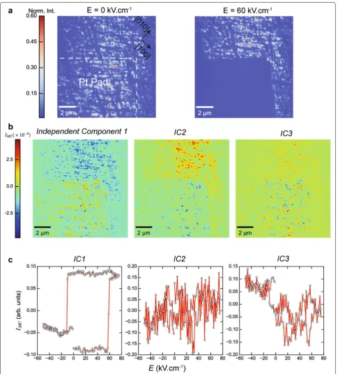
We repeated the same poling studies shown earlier, but instead acquired XDM images at a different scattering condition q=GBFO103. At this scattering condition, XDM imaging contrast is sensitive to both in-plane and out-plane changes in the structure of BFO. Given that the BFO film is strain relaxed and its polarization vector is along [ ¯111]¯ , we expect that the applied electric field (along [001]) will couple not only to piezoelectric coefficients along the c-axis (i.e., d33,dij is the piezoelectric strain tensor), but also to shear strains (e.g., d13) that we can image by XDM.
Remarkably, at a field of 65 kV cm−1 all contrast from
BFO domains underneath the Pt pad disappears entirely (Fig. 3a). Despite the presence of significant lattice rota-tions by epitaxial strain relaxation near the boundaries of the mosaic blocks, the polarization response of the sam-ple is found to be homogeneous over distances that are an order of magnitude larger than the size of a mosaic block. The field-dependent XDM data are analyzed by ICA with Fig. 3b, c displaying the spatial maps associated with the independent components and the latter’s dependence on the electric field, respectively. Similarly to the inde-pendent sources found in XDM data acquired at q002 , we find that one of the components produces the hysteresis loop (IC1) with identical physical properties such as the ferroelectric coercive fields (65, −15 kV cm−1) as well
Page 7 of 12 Laanait et al. Adv Struct Chem Imag (2017) 3:11
Fig. 3 Imaging the in‑plane piezoelectric response of BiFeO3. XDM images were acquired with q=GBFO103, during the poling cycle in Fig. 2a. Rep‑
resentative images taken at different values of the electric field during the cycle are shown in a. The dashed line represents the boundary of the Pt electrode. At E= 60 kV cm−1, the 103 Bragg planes of BFO underneath the electrode are rotated as a consequence of ferroelastic switching by shear
strains, and consequently they no longer satisfy the Bragg condition at q=GBFO
103 and appear in the XDM image with dark contrast (left panel). b
applied electric field, leading to ferroelastic switching. The changes in XDM imaging contrast due to these different material responses is indistinguishable, if measurements are taken at a single scattering vector q, as was performed
here. However, by independent reciprocal space measure-ments of the BFO 113 Bragg reflection as a function of electric field (see Additional file 1: Figure S2), we are able to determine that the observed changes in XDM contrast are mainly due to changes in d13.
Dynamic imaging of the piezoelectric response
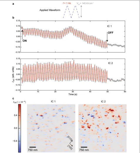
In addition to the static imaging presented so far, we dynamically imaged the field-driven structural responses of the film during the application of multiple triangular waveform cycles with varying frequencies. In Fig. 4a, an example of the applied waveform is shown while XDM images at the BFO 002 Bragg reflection were acquired at a frame rate of 5 Hz. This results in a time-dependent XDM set, X(r,t). Some of the information that can be extracted from this data is the nanoscale spatial inhomogeneity in the response of BFO domains, as well as temporal varia-tions in their response, for instance due to device fatigue or influence of localized defects near domain boundaries. As such, all of the presented dynamic data were taken on a pristine micro-capacitor and the total number of pol-ing cycles applied to the device was recorded. We extract these information channels by independent component analysis in the time-domain as follows:
where the independent components Si(t) now acquire time-dependence, and associated with each is a spa-tial feature map Ai(r). By decomposing X(r,t) into two
pure sources, we extracted the main characteristics of the applied waveform (i.e., frequency, slope) without a priori knowledge of the applied waveform. The observed oscil-lations in the intensity correspond to shifts in the scatter-ing angle 2θ due to the converse piezoelectric effect. We found two types of time-dependent piezoresponses in the BFO film, with IC2 showing a constant amplitude as a function of time that closely tracks the alternating field, while IC1 displays a response with an amplitude that is modulated over longer times (~10 s) but over shorter time scales displays the same frequency as IC1 and the applied waveform. Interestingly, the spatial feature map that is associated with IC1 shows that BFO domains whose piezoresponse is modulated with a longer period are largely oriented parallel to the miscut direction [110]. These modulations could be indicative of the presence of different strain gradients or local defects in BFO near
X(r,t)=
N
i=1
Ai(r)Si(t),
film domain boundaries oriented along the miscut direc-tion which would surely affect the piezoelectric response of the system.
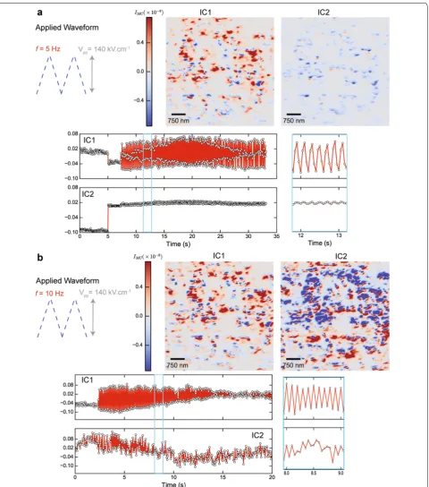
Following the same procedure as above, we applied waveforms with frequencies of 5 and 10 Hz, while cap-turing images at frame rates of 20 Hz (see Fig. 5a, b). In the first case (5 Hz), no transient dynamics were detected; the piezoelectric response of the film reflects one-to-one the field modulation (IC1). Note that this is in contrast to the behavior observed in the pristine state (Fig. 4b), and indicates that the modulated piezoelectric response found in Fig. 4b (top) is likely due to charge defects and not strain gradients due to this irreversible behavior. The second independent component describes the behavior of regions of the film that are on the order of ~100 nm that show no response to the electric field (IC2).
After poling the device continuously with nearly 3 × 10³ cycles, we applied a 10-Hz waveform (Fig. 5b).
During the first 5 s of poling the film, the measured pie-zoelectric response was synchronous with the waveform (as shown in the close-up). Progressively, however, the total amplitude of the response was observed to dimin-ish and became barely detectable at t > 12 s. Note that the spatial feature map of IC1 closely resembles that of IC1 from the 5-Hz waveform, indicating that no changes in the spatial configuration of BFO domains with strong piezoelectric response has occurred. Moreover, we find that much larger fluctuations in IC2 are present, as can be clearly seen by comparing their time series. Furthermore, the spatial features map (IC2 in Fig. 5b) now displays a much larger density of BFO domains whose response fluctuates substantially and in a transient fashion. These observations point to the onset of polarization fatigue, and was immediately confirmed by electrical measure-ments on this device, showing an increase of three orders of magnitude in resistance from ~100 MΩ to ~100 kΩ.
Discussion
Through the judicious application of model-independent matrix decomposition techniques, such as independ-ent componindepend-ent analysis, we were able to effectively mine the large datasets produced by XDM, thereby extract-ing many of the static physical characteristics of ferro-electric phenomena in bismuth ferrite thin-films such as the coercive fields, and to infer the presence of prefer-ential electrostatic screening at the Pt/BiFeO3 interface.
Page 9 of 12 Laanait et al. Adv Struct Chem Imag (2017) 3:11
Fig. 4 Dynamic imaging of the poling response. a An electric field modulated with a triangular waveform is applied across the BFO film. Simultane‑ ously, XDM images were acquired at q=GBFO
002 at a frame rate of 5 Hz. By decomposition of the XDM collection with ICA, the correct characteristics
Page 11 of 12 Laanait et al. Adv Struct Chem Imag (2017) 3:11
the miscut crystallographic orientation. After repeated polarization cycling, we were also able to detect the onset of transient piezoelectric switching that is indica-tive of the onset of polarization fatigue. In each case, spatially resolved maps of the changes in the structure of BFO, associated with each observed response, were also obtained, facilitating not only the interpretation of the observed phenomena but also served as a meaningful method by which to visualize the main spatial informa-tion that is essentially spread out over ~102–103 images,
each with 1024 × 1024 pixels.
The main advantage of the presented analysis is clearly its model-independent nature; no assumptions were made regarding the presence of: (i) hysteretic signals in the static imaging (Figs. 2, 3); (ii) oscillatory piezoelectric responses during the dynamic imaging (Figs. 4, 5). Note also that in each case of dynamic imaging, through the use of ICA we were able to extract the applied waveforms without implicit knowledge of the latter. More impor-tantly, the extracted material response signals were dis-cerned from spurious sources contained in the data, simply by their (linear) statistical independence, leading to the un-mixing of the two classes of signals and essen-tially producing material responses that are artifact-free. The latter is an important attribute of this decompo-sition technique, and one can therefore consider its application as an exploratory data mining technique in high-throughput X-ray imaging, followed by more phys-ics-based model-dependent analysis. Note that for nearly all matrix decomposition techniques their robustness and applicability can only be measured by their empiri-cal performance by subsequent comparisons to physics-based modeling to establish their utility in a particular class of problems.
The decorrelation of extrinsic sources from intrinsic signals present in the large datasets produced by full-field X-ray diffraction microscopy is an indispensable component in further development of X-ray diffrac-tion-based imaging techniques and their application to materials physics. By their very nature, synchrotron sources are noisy environments, and consequently an X-ray microscope that extends over tens of meters (from monochromator to detector) in this environment will invariably produce datasets that contain extrinsic signals. These signals have been consistently identified in the presented results (e.g., Fig. 2d) and can consist of increased variations in the spatial distributions of the X-ray beam or mechanical instabilities. It would be interesting in future work to incorporate matrix decom-position models that explicitly incorporate different noise models (e.g., noisy ICA [28]) for a more robust un-mixing of material responses from instrumental responses.
Conclusion
We have presented full-field Bragg diffraction imaging studies of the field-driven responses in epitaxial thin-films at unprecedented spatiotemporal resolutions. We also demonstrated how model-independent analysis techniques facilitate mining these immense datasets for the salient material responses and their spatiotemporal evolution. Future developments in this type of microscopy and asso-ciated data-intensive algorithms to mine its large datasets, promise to enable access to a host of field-driven structural responses in materials at the nanoscale and in real-time.
Abbreviations
XDM: X‑ray diffraction microscopy; ICA: independent component analysis; STO: SrTiO3; BFO: BiFeO3; SRO: SrRuO3.
Authors’ contributions
NL conceived and designed the research, and performed the analysis. NL, HZ, and ZZ performed the X‑ray measurements. WS and CBE synthesized the samples and fabricated the devices. NL wrote the manuscript with input from all the authors. All authors read and approved the final manuscript.
Author details
1 Center for Nanophase Materials Sciences, Oak Ridge National Laboratory,
Oak Ridge, TN 37831, USA. 2 Institute for Functional Imaging of Materials, Oak
Ridge National Laboratory, Oak Ridge, TN 37831, USA. 3 Department of Materi‑
als Sciences and Engineering, University of Wisconsin‑Madison, Madison, WI 53706, USA. 4 X‑ray Science Division, Argonne National Laboratory, Lemont, IL
60439, USA.
Acknowledgements Not applicable.
This manuscript has been authored by UT‑Battelle, LLC under Contract No. DE‑AC05‑00OR22725 with the U.S. Department of Energy. The United States Government retains and the publisher, by accepting the article for publication, acknowledges that the United States Government retains a non‑ exclusive, paid‑up, irrevocable, world‑wide license to publish or reproduce the published form of this manuscript, or allow others to do so, for United States Government purposes. The Department of Energy will provide public access to these results of federally sponsored research in accordance with the DOE Public Access Plan (http://energy.gov/downloads/doe‑public‑access‑plan).
Competing interests
The authors declare that they have no competing interests.
Availability of data and materials
Data are available upon request from N. Laanait ([email protected]).
Funding
This work was supported by the Eugene P. Wigner Fellowship program (NL) at Oak Ridge National Lab. The work at University of Wisconsin‑Madison (C‑B. Eom) was supported by the Army Research Office through grant W911NF‑13‑1‑0486.
Received: 25 October 2016 Accepted: 26 February 2017 Additional file
Additional file 1: Figure S1. Reciprocal space mapping of BiFeO3/
SrRuO3/SrTiO3 at the 103 and 113 Bragg reflection in the pristine state
(i.e., zero applied electric fields). Figure S2. Reciprocal space mapping of BiFeO3/SrRuO3/SrTiO3 at the 113 Bragg reflection as a function of applied
References
1. Pennycook, S.J., Kalinin, S.V.: Microscopy: Hasten high resolution. Nature
515, 487–488 (2014)
2. Holt, M., et al.: Nanoscale hard X‑ray microscopy methods for materials studies. Annu. Rev. Mater. Res. 43(1), 183–211 (2013)
3. Li, L., Jokisaari, J.R., Pan, X.: In situ electron microscopy of ferroelectric domains. MRS Bull. 40(1), 53–61 (2015)
4. Ice, G.E., Budai, J.D., Pang, J.W.L.: The race to X‑ray microbeam and nano‑ beam science. Science 334(6060), 1234 (2011)
5. Cartlidge, E.: European XFEL to shine as brightest, fastest X‑ray source. Science 354(6308), 22 (2016)
6. Miao, J., et al.: Beyond crystallography: diffractive imaging using coherent X‑ray light sources. Science 348, 530–535 (2015)
7. Evans, P.G., et al.: X‑ray microdiffraction images of antiferromagnetic domain evolution in chromium. Science 295, 1042–1045 (2002) 8. Hofmann, F., Abbey, B., Liu, W., Xu, R., Usher, B.F., Balaur, E., Liu, Y.: X‑ray
micro‑beam characterization of lattice rotations and distortions due to an individual dislocation. Nat. Commun. 4, 2774 (2013). doi:10.1038/ ncomms3774
9. Larson, B.C., et al.: Three‑dimensional X‑ray structural microscopy with submicrometre resolution. Nature 415(6874), 887–890 (2002) 10. Holt, M.V., et al.: Strain imaging of nanoscale semiconductor heterostruc‑
tures with X‑ray bragg projection ptychography. Phys. Rev. Lett. 112(16), 165502 (2014)
11. Hruszkewycz, S.O., et al.: Imaging local polarization in ferroelectric thin films by coherent X‑ray Bragg projection ptychography. Phys. Rev. Lett.
110, 177601 (2013)
12. Laanait, N., et al.: Full‑field X‑ray reflection microscopy of epitaxial thin‑ films. J. Synchrotron Radiat. 21(6), 1252–1261 (2014)
13. Simons, H., et al.: Dark‑field X‑ray microscopy for multiscale structural characterization. Nat. Commun. 6, 6098 (2015)
14. Fenter, P., et al.: Observation of subnanometre‑high surface topogra‑ phy with X‑ray reflection phase‑contrast microscopy. Nat. Phys. 2(10), 700–704 (2006)
15. Laanait, N., et al.: X‑ray‑driven reaction front dynamics at calcite‑water interfaces. Science 349(6254), 1330–1334 (2015)
16. Laanait, N., Zhang, Z., Schlepütz, C.M.: Imaging nanoscale lattice varia‑ tions by machine learning of X‑ray diffraction microscopy data. Nano‑ technology 27(37), 1–10 (2016)
17. Baek, S.H., et al.: Ferroelastic switching for nanoscale non‑volatile magne‑ toelectric devices. Nat. Mater. 9(4), 309–314 (2010)
18. Das, R.R., et al.: Synthesis and ferroelectric properties of epitaxial BiFeO3
thin films grown by sputtering. Appl. Phys. Lett. 88(24), 242904 (2006) 19. Eom, C.B., et al.: Epitaxial thin films of the isotropic metallic oxides. Sci‑
ence 258(5089), 1766 (1992)
20. Schlepütz, C.M., et al.: Angle calculations for a (2 + 3)‑type diffractometer: focus on area detectors. J. Appl. Crystallogr. 44, 73–83 (2010)
21. Zavaliche, F., et al.: Multiferroic BiFeO3 films: domain structure and polari‑
zation dynamics. Phase Transit 79(12), 991–1017 (2006)
22. Streiffer, S.K., et al.: Domain patterns in epitaxial rhombohedral ferroelec‑ tric films. I. Geometry and experiments. J. Appl. Phys. 83(5), 2742–2753 (1998)
23. Fong, D.D., et al.: Stabilization of monodomain polarization in ultrathin PbTiO3 films. Phys. Rev. Lett. 96(12), 127601 (2006)
24. Christen, H.M., et al.: Stress‑induced R‑MA‑MC‑T symmetry changes in BiFeO3 films. Phys. Rev. B 83(14), 144107 (2011)
25. Streiffer, S.K., et al.: Domain patterns in epitaxial rhombohedral ferro‑ electric films. I. Geometry and experiments. J. Appl. Phys. 83, 2742–2753 (1998)
26. Physics of ferroelectrics: a modern perspective, 1st ed. Springer Publish‑ ing Company, Incorporated, Berlin (2007)
27. Goodman, J.W.: Introduction to Fourier optics, 3rd ed. Roberts & Co, Englewood (2005)
28. Hyvärinen, A., Karhunen, J., Oja, E.: Independent component analysis, vol. 46. Wiley, New York (2004)
29. Hastie, T., Tobshirani, R., Friedman, J.: The elements of statistical learning: data mining, inference, and prediction. In: Springer Series in Statistics. Springer Science + Business Media, New York (2009)
30. Vigário, R., et al.: Independent component analysis for identification of artifacts in magnetoencephalographic recordings. In: Advances in neural information processing systems. MIT Press, Cambridge (1998)
31. Back, A.D., Weigend, A.S.: A first application of independent component analysis to extracting structure from stock returns. Int. J. Neural Syst. 8(4), 473–484 (1997)