Highly Efficient Grating Coupler for SOI Integrated
Photonics label free Bio-sensing Application
Mohammad Mohiuddin Uzzal
Electrical and Electronic Engineering, Ahsanullah University of Science and Technology (AUST), Dhaka, Bangladesh Email: [email protected]
Abstract- Integrated photonics based on silicon on insulator (SOl) using CMOS manufacturing process is a promising candidate for level free bio-sensing application. In this article we discuss on the principle and importance of level free bio-sensing. Then we present the design process and the finite difference time domain (FDTD) simulation result of building blocks for a typical optical ring resonator based integrated photonic bio-sensor operating at 1550nm. The resonance frequency of the design is 1550nm which experiences very low loss. Our designed ring has a radius of 10um, coupling gap between ring and waveguide of 150nm and waveguide width of 500nm. Input grating coupler has a period of 600nm with duty cycle of 0.67. The grating height is 175nm with 38 total periods. The output coupler has filling factor of 0.35 and period of 550nm with grating height of 250nm. There are total 25 periodic structure at output coupler. The SOI wafer has a silicon thickness of 340nm and buried oxide layer thickness of 1000nm. The overall efficiency of the grating coupler from input to output of the sensor is 42 percent.
Index Term— Label free, bio-sensor, ring resonator, coupling, optical sensor, Grating Coupler, Integrated Photonics, bio fictionalization, FDTD
I. INTRODUCTION
Due to the high refractive index contrast, Silicon-on-Insulator (SOI) technology is an attractive platform for compact integrated photonic circuits. SOI is also CMOS compatible and has created widespread interest not only in the photonics community, but also in the electronics world to integrate photonic functions in the next generation of high speed processors. However, efficient coupling in and out of a silicon circuit remains a challenge, due to a huge mismatch between the optical fiber mode and the nano-photonic waveguide mode [1]. Several attempts were made to find a solution to this problem. Grating couplers are an attractive solution, since light can be coupled out of plane through vertical coupling.
Having fast, efficient, and reliable sensing devices is essential in many fields, such as medical diagnostics, food safety control, environmental control, and drug detection [2]. Optical biosensors are a powerful detection and analysis tool that has vast applications in biomedical research, healthcare, pharmaceuticals, environmental monitoring, homeland security, and the battlefield. They are immune to electromagnetic interference, capable of performing remote sensing, and can provide multiplexed detection within a single device. Generally, there are two detection protocols that can be implemented in optical bio-sensing: fluorescence-based detection and label-free detection. In fluorescence-based
detection, either target molecules or bio-recognition molecules are labeled with fluorescent tags, such as dyes; the intensity of the fluorescence indicates the presence of the target molecules and the interaction strength between target and bio-recognition molecules. While fluorescence-based detection is extremely sensitive, with the detection limit down to a single molecule, it suffers from laborious labeling processes that may also interfere with the function of a biomolecule. In contrast, in label-free detection, target molecules are not labeled or altered, and are detected in their natural forms. Label free optical biosensors are becoming more and more important as they facilitate real time monitoring with high sensitivity. This type of detection is relatively easy and cheap to perform, and allows for quantitative and kinetic measurement of molecular interaction. Additionally, some label-free detection mechanisms measure refractive index (RI) change induced by molecular interactions, which is related to the sample concentration or surface density, instead of total sample mass. As a result, the detection signal does not scale down with the sample volume. This characteristic is particularly attractive when ultra-small detection volume is involved and is advantageous over fluorescence-based detection whose signal usually depends on the total number of analytes in the detection volume or on the detection surface.
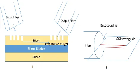
Fig. 1. Illustration of Integration of Light on SOI technology 1) Vertical coupling through grating coupler 2) Butt/edge coupling
In this paper, we present the design of an integrated photonics bio-sensor based on SOI ring resonator and grating coupler. In Section II, we discuss of fiber to SOI chip light coupling problem. In Section III, we give an overview on bio-sensing based on SOI ring resonator. The details design of the SOI integrated Bio-sensor is presented in Section IV. Section V gives an introduction on FDTD simulator. Finally, the conclusion is discussed in Section VI.
II. FIBER TO CHIP COUPLING PROBLEM
Conventional single mode SOI strip waveguides are about 220 nm thick and 500 nm wide. Because of their small dimensions, and also because the related fabrication tolerances are in the nanometer range, we use the term nano-photonic waveguides. However, standard single mode fibers (SMF) are very large size compared to nano-photonic SOI waveguides. Typical core diameter size of a standard SMF is about 8μm. Thus, injecting (coupling) light from an optical fiber to a nano-photonic waveguide becomes a difficult task as depicted in Figure 1. The high difference in the dimensions between the fiber and the waveguide causes a high mismatch between their optical modes. Due to this mismatch, a coupling structure is needed to adapt a wide fiber to a narrow silicon waveguide improving the coupling loss. Typically, a direct butt coupling between a single mode fiber (mode field diameter MFD=10 μm) and a nano-photonic waveguide (MFD <1 μm) leads to more than 20dB insertion (coupling) loss [13].
In vertical coupling through grating coupler, light is injected onto the surface of the waveguide at a specific angle, vertically. A grating coupler, is basically a one dimensional (1D) diffractive structure that can be designed for coupling light onto the waveguide surface by means of one of its orders of diffraction. Even though grating couplers are relatively narrowband in comparison with edge coupling, they provide additional benefits. The first advantage is the simplicity of fabrication. The grating couplers can be defined in the same process module as other photonic devices. This module comprises a lithography and an etch step and leads to significantly lower cost than other approaches that employ exotic and complex processing. An obvious benefit of vertical coupling is that it provides flexibility in placing the optical interface anywhere on the chip surface. This allows increasing the density of optical interfaces and frees the chip edge to be used for low- and high-speed electrical signal pads. Surface
before costly packaging steps. Another major cost advantage is the elimination of polishing and other surface preparation steps. Finally, grating couplers are fully CMOS compatible and have been used in commercial products based on CMOS photonics dies [14]. Grating coupler based coupling is the solution to overcome the integration issue in fiber-chip coupling scenario.
III. WORKING PRINCIPLE OF SOIINTEGRATED BIO-SENSOR This SOI ring resonator based sensing technique works on sensing of spectral shift with background refractive index change. The spectral shift is due to interaction of evanescent field with the medium. The more the interaction with the evanescent field the more is the spectral shift and the more sensitive the sensor becomes.
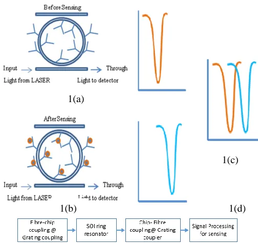
Figure 2, shows the working principle of evanescent based sensing principle in details. Here, Bio-recognition molecules, such as antibodies are immobilized onto the surface of the waveguide. The evanescent field of the guided light in the waveguide extends into the surrounding medium and interacts with the bio-molecules near the waveguide surface. A small change in refractive index near the waveguide surface when target analytes are captured causes modifications in the optical signal at the output, which acts as the sensing signal. Since the sensing signal is accumulative in nature, a longer light-analyte interaction length results in a higher sensitive sensor. In contrast to the straight waveguide, the effective light–analyte interaction length of a ring resonator sensor is no longer determined by the sensor’s physical size, but rather by the number of revolutions of the light supported by the resonator, which is characterized by the resonator quality factor, or the Q-factor. The effective length, Leff, is related to the Q-factor by: Leff =Qλ/2∏n, where λ is the resonant wavelength and n is the RI of the ring resonator [2]. The higher the Q factor the better is the sensor precision in determination of spectral shift.
From the shift in resonance point due to effective refractive index change, the concentration of the analyte and kinetic information about the binding of the analyte to the receptor can be determined. Typically, a Lorentzian function is fitted to each measured resonance dip or peak in order to precisely determine the resonance wavelength. Our focus in this paper is the design and simulation of a low loss SOI optical micro-ring resonator for label free bio-sensing application.
IV. DESIGNDIMESIONSANDFDTDSIMULATION
RESULTS
A. OPTICAL RING RESONATOR:
Fig. 2. Evanescent wave based sensing principle using SOI optical micro ring resonator. 1(a) shows the sensing structure and spectral response before sensing. 1(b) shows the sensing structure and the spectral response after sensing 1(c) shows the relative position of the two spectrum and also the resulting shift due to attachment of bio-molecules on sensor surface and 1(d)
summarizes the signal flow during SOI ring resonator based integrated photonic bio-sensing.
When light of desired wavelength that can produce resonance, is passed through the optical ring loop, intensity is enhanced after the multiple round trips because of constructive interference. This Optical sensor with known frequency response can be used as add-drop filters, switches, isolators, delay line, memory devices, logic gates, environmental sensors, bio-sensors, mechanical sensors etc. Optical coupling of the sensor can be controlled by three controlling parameters -1) distance - with this optical coupling is inversely proportional, 2) coupling length - with it optical coupling is directly proportional and 3) Refractive Index between the waveguide and optical resonator [12].
Fig. 3. Top view of the SOI ring resonator. Ring is separated from the wave-guide by a gap d. C-C’ is the plane for cross-sectional view at figure (3)
Fig. 4. Cross-sectional view of the designed SOI ring resonator. The coupling gap, d=150nm , waveguide width, w=500nm, Si layer thickness is 340nm and
Oxide layer thickness is 1000nm and the ring Radius R=10um
If the ring and the waveguide are close enough, the light in the waveguide will be transmitted into the ring. There are three aspects that affect the optical coupling: i) the distance, ii) the coupling length and iii) the refractive indices between the waveguide and the optical ring resonator. In order to optimize the coupling, it is usually the case to narrow the distance between the ring resonator and the waveguide. The closer the distance, the easier the optical coupling happens. The coupling length represents the effective curve length of the ring resonator for the coupling phenomenon to happen with the waveguide. Generally as the optical coupling length increases, the difficulty with the coupling to happen decreases. The refractive index of the waveguide material, the ring resonator material and the medium material in between the waveguide and the ring resonator also affect the optical coupling. The medium material is usually the important one been studied since it has a great effect on the transmission of the light wave. The refractive index of the medium can be either large or small according to various applications and purposes.
The behavior of optical ring resonator is dictated by the following equations. The Quality factor, Q of the ring resonator determines how precisely the resonance wavelength can be measured and hence the shift from the sensing application. Generally, the higher the Q -factor, the better is the resonator. For a ring resonator Leff is very high as the optical wave circulates across the ring for numerous times and makes Q very high with a very small physical dimension.
)
2
4
1
arccos(
2
2
)
(
2 20 3
0
t
t
t
L
n
Q
gr effdb
…….(1)where λ0 is the resonant wavelength, ngr is the group index,
Leff is the effective length, τ is the field attenuation and ׀t׀ is
the field transmission coefficient.
Free spectral range (FSR) is the distance between resonance peaks or dips. It depends on the radius of the ring as well as wavelength. Generally, the lower the radius of the ring the higher is the free spectral range and for micro resonator FSR is very high.
1(a)
1(b)
1(c)
Fig. 5. LUMERICAL finite difference time domain (FDTD) simulation setup of the Grating Coupler for Integrated Photonic Applications
Fig. 6. Input coupling efficiency of grating coupler as the position of the Optical source is varied.
R
n
FSR
gr
2
2
….. …… …………...…. …… (2)
Where R is the radius of the ring, λ is the operating wavelength and ngr is the group index
The group index ngr takes into account the dispersion of the waveguide and is defined by –
d
dn
n
n
gr
eff
0 eff ………(3)Where neff is the effective refractive index, λ0 is the resonant wavelength
B. GRATING COUPLER:
The simplest coupler design is based on a grating that is periodic in one dimension along the propagation of the light in the waveguide. Figure 5 shows a schematic cross-sectional view of a grating coupler as input to LUMERICAL FDTD simulator. As light propagates through the grating, it is scattered coherently toward an angle-polished fiber with its polished face parallel to the chip.
The design process on a CMOS photonics platform must carefully balance performance with manufacturability. Once the wafer structure and the etch depth are chosen, there are
grating, and the layout of the grating in the direction perpendicular to the propagation of the light.
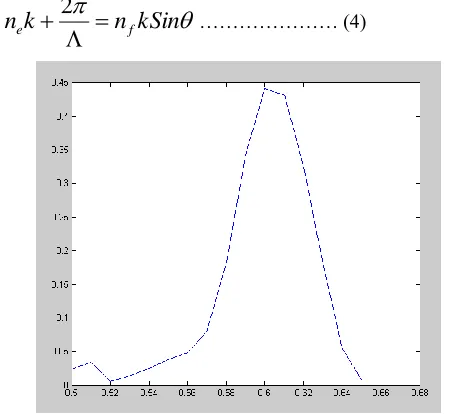
The grating periodicity determines the phase-matching condition to the fiber mode that is incident on the surface of the chip at a certain angle. Let us denote the effective index of the mode propagating inside the grating by ne, the effective index of the fiber mode by nf , the pitch of the grating by Λ, the free-space wavevector by k = 2π/λ, where λ is the free free-space wavelength, and the angle enclosed by the optical axis of the fiber and the normal to the chip by θ. The phase matching condition then can be written as follows [14]:
kSin
n
k
n
e
f
2
……… (4)Fig. 7. Coupling efficiency as the period of the grating structure is varied. It illustrates that a maximum coupling efficiency occurs at 60% grating period.
Fig. 9. Number of Period Vs Coupling efficiency. It illustrates that as the period no increases, efficiency increases BUT optimum is need for space and
cost.
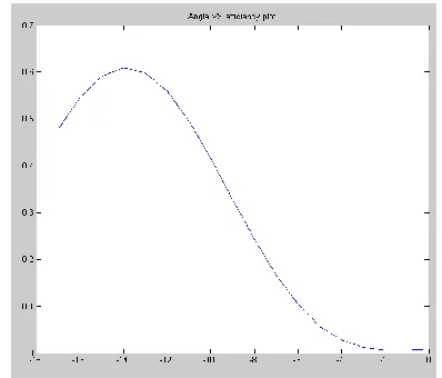
Fig. 10. Optical source insertion angle VS efficiency. It shows that maximum efficiency occurs at 14 degree insertion angle.
There are several considerations when selecting the optimal fiber angle. Importantly, we must consider how the light that is scattered by the grating propagates through the dielectric backend present on the CMOS chip. For even simple electronic circuits, there are six to ninemetal layers needed for connections between the circuit building blocks and subcircuits as well as for top-level routing. These metal interconnects are embedded in dielectric layers that are made of different types of silicon nitride and oxide materials. Although these materials are transparent at optical communication wavelengths, their refractive indices vary from layer to layer.
Fig. 11. Coupling efficiency (optical light intensity along the grating coupler after efficient coupling)
Fig. 12. Filling factor VS efficiency of output grating coupler
Fig. 13. Grating period VS efficiency of output grating coupler
A uniform grating produces an exponential scattered intensity profile, with a maximum theoretical efficiency of approximately 80%. Therefore, we can expect that a nonuniform, or apodized, grating can increase the coupling efficiency by up to 1 dB.
However, the available design space is restricted by the capability of the lithography node available in the CMOS process. The process is capable of producing features only down to a minimum size specified by a design rule. If the device utilizes features below this feature size, it will be susceptible to process excursions, where for some process corners, the device performance can be significantly degraded.
formulation in [16]. Mathematical theorems for the FDTD formulation, concerning issues such as accuracy, convergence, dispersion, computational complexity and stability are provided in [17] and [18]. The FDTD method has been extensively applied to simulate and analyze WGM of isolated micro-disks, micro-disks and micro-rings. The general FDTD simulation method considers a two-dimensional (2D) problem where the z-directed optical field is normal to the x-y plane of the grid. In the simulation, the perfectly matched layer (PML) absorbing boundary condition (ABC) were introduced, providing the means to terminate the calculated grid space with extremely low reflection [19]. The accuracy of the FDTD method for problems in linear optics was first demonstrated for the directional coupler [20].
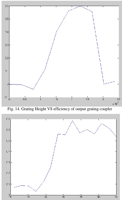
Fig. 14. Grating Height VS efficiency of output grating coupler
Fig. 15. Number of period VS efficiency of Output grating coupler
For accurate FDTD simulations, there are some challenges that we should note: (i) The computation time required for accurate simulation of light recirculation in WGM cavities is
numerical boundary conditions is very small within PML ABC, its effects can adversely affect the simulation results. The errors in FDTD simulations are negligibly small if the grid size of the computing space is on the order of λ/10 to λ/20 and this requirement is valid only for simulation of simple systems such as scattering problems in which there is no recirculation of resonant light. Generally, the smaller the grid size is, the better the results. But tradeoff is the simulation time goes up as the grid size goes down [21].
We had optimized our design in LUMERICAN FDTD and the optimization process of the design is shown in Figure 6, 7, 8, 9, 10, 11, 12, 13, 14, 15, 16 and 17. The simulation result shows that there are some optimum value that gives us the maximum efficiency in coupling. The optimum design dimensions are summarized below:
Fig. 16. Intensity of light along the output grating coupler
Fig. 17. Through port and drop port transmission spectrum of the Optical ring resonator. We can see that resonance occurs only at certain frequency and the
FSR (distance between two resonance wavelength) of the ring.
Input Grating Coupler: i) duty cycle 0.67 ii) grating height 175nm iii) grating period 600nm iv) total period 38
Output Grating Coupler: i) filling factor 0.35 ii) grating period 550nm iii) grating height 225nm iv) total period 25
Drop port Spectrum Through Port Spectrum
Wavelength (nm)
M
a
g
nitude (
o
utput
/in
pu
Photonic Ring Resonator: i) ring radius 10um ii) Coupling gap 150nm iii) waveguide width 500nm
Our FDTD simulation result shows that the input grating coupler gives us a coupling efficiency of 60% whereas the output grating coupler’s efficiency is 70%. Therefore the overall efficiency from the integrated grating coupler (from input to output) is about 42%.
VI. CONCLUSION
Grating couplers are essential building blocks in CMOS photonics circuits and provide an attractive option over edge coupling schemes. Edge-coupling approaches have inherent cost implications, such as process complexity, accurate dicing requirements, and optical-grade facet polishing. In addition, breaking the guard ring of the CMOS chip introduces reliability risks. In summary, here we present the design, simulation results of grating coupler that are essential for integrated photonic sensor frequently used in bio-sensing application. The coupling efficiency that we get from input to output of the bio-sensor through grating coupler is 42%. The SOI ring resonator which is an integral part of this integrated photonic sensor, has a radius of 10um and so an area of approximately 400um2. So the required footprint for sensing is ultra low amount and hence it is very suitable for sensing of analytes whose sample size is very small i.e. DNA, RNA, blood etc.
REFERENCES
[1] S.K. Selvaraja et.al.,"Highly efficient grating coupler between optical fiber and silicon photonic circuit",Department of Information Technology, Gent, Belgium
[2] Xudong Fan, Ian M. White, Siyka I. Shopova, Hongying Zhu,Jonathan D. Suter, Yuze Sun -"Sensitive optical biosensors for unlabeled targets: A review" - analytica chimica acta ( 2008 )
[3] M. E. Stewart, C. R. Anderton, L. B. Thompson, J. Maria, S. K. Gray, J. A. Rogers, and R. G. Nuzzo, “Nanostructured plasmonic sensors,” Chem. Rev. 108(2), 494–521 (2008).
[4] J. Homola, Surface Plasmon Resonance Based Sensors (Springer, 2006). [5] B. J. Luff, J. S. Wilkinson, J. Piehler, U. Hollenbach, J. Ingenhoff, and N. Fabricius, “Integrated Optical Mach–Zehnder Biosensor,” J. Lightwave Technol. 16(4), 583–592 (1998).
[6] A. Brandenburg, “Differential refractometry by an integrated-optical Young interferometer,” Sens. Actuator B-Chem. 39(1-3), 266–271 (1997)
[7] M. E. Bosch, A. J. Ruiz Sánchez, F. S. Rojas, and C. B. Ojeda, “Recent Development in Optical Fiber Biosensors,” Sensors (Basel Switzerland) 7(6), 797–859 (2007)
[8] D. J. Monk and D. R. Walt, “Optical fiber-based biosensors,” Anal. Bioanal. Chem. 379(7-8), 931–945 (2004)
[9] B. Cunningham, P. Li, B. Lin, and J. Pepper, “Colorimetric resonant reflection as a direct biochemical assay technique,” Sens. Actuator B-Chem. 81(2-3), 316–328 (2002)
[10] M. R. Lee and P. M. Fauchet, “Two-dimensional silicon photonic crystal based biosensing platform for protein detection,” Opt. Express 15(8), 4530–4535 (2007).
[11] F. Vollmer and S. Arnold, “Whispering-gallery-mode biosensing: label-free detection down to single molecules,” Nat. Methods 5(7), 591–596 (2008).
[12] D.-X. Xu, M. Vachon, A. Densmore, R. Ma, A. Delâge, S. Janz, J. Lapointe, Y. Li, G. Lopinski, D. Zhang, Q. Y. Liu, P. Cheben, and J. H. Schmid, “Label-free biosensor array based on silicon-on-insulator ring resonators addressed using a WDM approach,” Opt. Lett. 35(16), 2771– 2773 (2010)
[13] F.V.Laere et. al.,"Compact and Highly Efficient Grating Couplers Between Optical Fiber and Nanophotonic Waveguides", Journal of Lightwave Technology, Vol. 25, No. 1, Jan 2007, pp.151-156
[14] Attila Mekis et.al.,"A Grating-Coupler-Enabled CMOS Photonics Platform", IEEE Journal of selected topics in Quantum Electronics, Vol. 17, No. 3, May 2011, pp. 597-608
[15] Ishita Bharl, Tapolina Jha, Priya,Sabitabrata Dey, "Design and Simulation of Integrated Optic Ring Resonator based Devices" 2012 International Conference on Communications, Devices and Intelligent Systems (CODIS), pp. 453-456
[16] Yee, K. S., “Numerical solution of initial boundary value problems involving Maxwell’s equations in isotropic media,” IEEE Trans. Antennas and Propagation, Vol. 14, 302–307, May 1966.
[17] Taflove, A., Computational Electrodynamics- The finite differencetime-domain method, Artech House, 1995.
[18] Strikwerda, J. C., Finite Difference Schemes and Partial Differential Equations, Wadsworth & Brooks/Cole Mathematics Series, 1989. [19] J.-P. Berenger “A perfectly matched layer for the absorption of
electromagnetic waves,” J.Comput Phys. 114(2), 185–200 (1994) [20] S.-T. Chu and S. K. Chaudhuri, “A finite-difference time-domain
method for the design and analysis of guidedwave optical structures,” J. Lightwave Technol. 7(12), 2033–2038 (1989)