Process Variation Aware Transistor Sizing for
Load Balance of Multiple Paths in Dynamic
CMOS for Timing Optimization
Kumar Yelamarthi and Chien-In Henry Chen
Department of Electrical Engineering, Wright State University, Dayton, OH, USA Email: {yelamarthi.2, henry.chen}@wright.edu
Abstract— The complexity in timing optimization of high-performance microprocessors has been increasing with the number of channel-connected transistors in various paths of dynamic CMOS circuits and the rising magnitude of process variations in nanometer CMOS process. In this paper, a process variation aware transistor sizing algorithm for dynamic CMOS circuits while considering the Load Balance of Multiple Paths (LBMP) is proposed. The proposed iterative optimization algorithm is a deterministic approach and is illustrated first by a 2-b weighted binary-to-thermometric converter (WBTC) and of which the critical path was optimized from an initial delay of 355 ps to an optimal delay of 157 ps, which accounts for a 55.77% delay improvement. A 4-b unity weight binary-to-thermometric converter (UWBTC) was also designed and of which the critical path was optimized from an initial delay of 152 ps to an optimal delay of 103 ps, which accounts for a 32.23% delay improvement. Finally, a 64-b parallel binary adder was partitioned to a mixed dynamic-static CMOS style and the critical path and the power delay product were optimized to 632 ps and 84.17 pJ respectively.
Index Terms— dynamic CMOS logic, transistor sizing, timing optimization, process variations, binary-to-thermometer decoder, parallel binary adders.
I. INTRODUCTION
The performance of microprocessors has been driven traditionally by dynamic CMOS technology and micro architectural improvements [1], and can be enhanced at the circuit level through design and physical organization. At the circuit level, dynamic logic style has been pre-dominantly used in microprocessors, and the use of custom dynamic circuits in microprocessors has increased timing performance significantly over static CMOS circuits [1-2]. One of the challenges in timing optimization of dynamic CMOS circuits is transistor sizing due to charge sharing, noise-immunity, process variations and leakage, etc.
Research has demonstrated that process variations have caused about 30% variation in chip frequency, along with 20X variation in chip leakage [17]. Integrated circuits have always been vulnerable to inherent die-to-die (inter-die-to-die) and within-die-to-die (intra-die-to-die) parameter variations during the fabrication process [12]. With the
continued scaling of CMOS technology towards the 45 nanometer (nm) transistor channel length, the magnitude of relevant sources of environmental and semiconductor process variations have been increasing rapidly. This increased magnitude of process variations could lower the performance of a circuit by one generation [12], and might even result in design failure [13]. The magnitude of intra-die channel length variations has been estimated to increase from 35% of total variation in 130 nm, to 60% in 70 nm CMOS process. And, variations in wire width, height, and thickness are also estimated to increase from 25% to 35% at the 70nm CMOS process [13].
Transistor sizing and optimization affects delay and power of dynamic CMOS logic. However, designs optimized for power by transistor sizing are more susceptible to frequency impact due to within-die variations as they sharpen path delay distributions making a large number of paths and transistors critical [20]. This further highlights the importance of considering process variations while optimizing delay and power.
II. PREVIOUS WORK
Many literatures exist on automating transistor sizing [3-9]. Most of the proposed methods focus on static CMOS circuits and technologies using multiple threshold voltages. TILOS [4] presented an algorithm used for iteratively sizing transistors by a factor in the critical path. This algorithm does not guarantee a convergence of timing optimization and is not a deterministic approach. MINFLOTRANSIT [5] is an algorithm proposed for transistor sizing based on iterative relaxation method but requires generation of directed acyclic graphs iteratively for timing optimization.
method does not address the intra-die variations issue as each block in the design requires a unique bias voltage. Another limitation of this method is the increased leakage power due to reduction of threshold voltage. Using keepers to compensate for process variations was proposed in [18]. This method works for designs with large number of parallel stacks similar to NOR gates, but is not optimal for designs without parallel stacks as it requires additional hardware to program the keeper transistors.
Selecting multiple corners to simulate a design accounts for systematic variations but not random variations. Monte Carlo method considers both systematic and random variations [23]. As variations in
D
L and WDare random and predicted to be major contributors towards total variations [13], Monte Carlo simulation results are promising when delay is the constraint. Although there are misconceptions that Monte Carlo method is slow, it is ideal when the number of sources of variations is significantly high [21]. The advantage of using Monte Carlo method is its theoretical accuracy. This method is also commonly used as a golden reference. Monte Carlo method can be used to clearly explain the behavior of a circuit. It can be easily extended to incorporate crosstalk and IR drop effects in simulation [21].
Research has shown intra-die variations primarily impact the mean delay, and inter-die variations primarily impact the variance of delay [12]. So, design tools aimed towards optimization of timing and yield should consider both inter-die and intra-die variations. In addition to timing optimization by reducing delay, performance has to be improved by reducing the delay uncertainty and sensitivity due to process variations as depicted in (1) and (2), where TMax is the worst-case delay and TMin is the
best-case delay, ȝ is the mean delay, ı is the standard deviation from Monte Carlo simulations.
Tuncertainty TMaxTMin (1) Ws V/P (2)
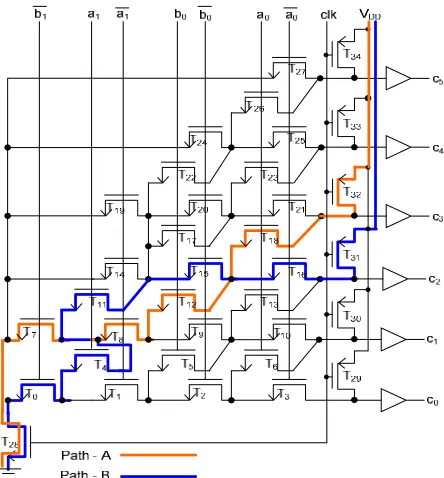
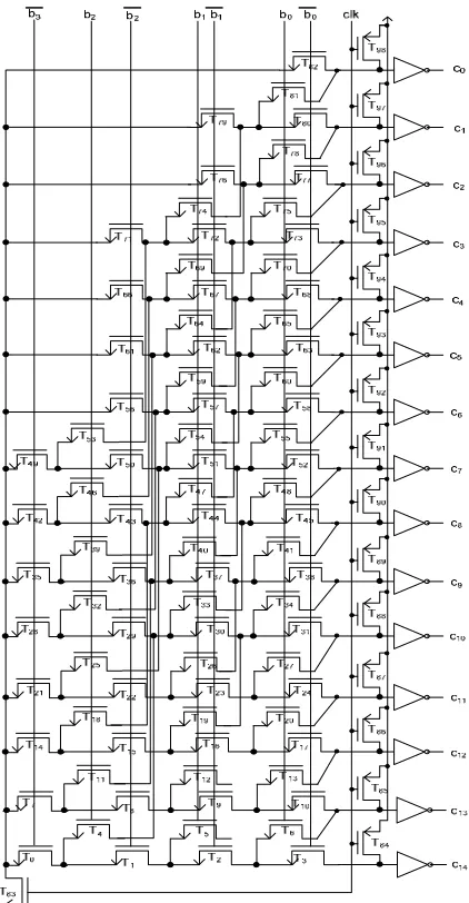
III. LOAD BALANCE OF MULTIPLE PATHS (LBMP) The delay of dynamic CMOS circuit is highly dependent on the number and size of transistors in the critical path. Increasing size of transistors in a path will increase the discharging current and reduce the output pull-down path delay. However, increasing the size of transistors to reduce one path delay may also increase the capacitive load of channel-connected transistors on other paths and substantially increase delays of respective paths. This level of complexity increases along with the number of paths in the design. In this paper, a 2-b Weighted Binary-to-Thermometric Converter (WBTC) as shown in Fig. 1 is used as a first benchmark to explain the path delay optimization complexity while considering process variations.
Fig. 1 highlights two timing paths: path-A (T28 -T7 - T8
- T12 - T18 – T32) and path-B (T28 - T0 - T4 - T11 - T15 – T16
– T31). A test was performed to optimize path-A by
gradually increasing sizes of T7, T8, T12 and T18. It was
observed that the delay of path-A reduced by 4%, but delay of path-B increased by 9.3%. This is a result of transistors on path-B being channel-connected to transistors on path-A. For instance, T4 and T11 are
channel-connected to T7 and T8, and T15 and T16 are
channel-connected to T12 and T18. Increasing widths of
T7, T8, T12 and T18 in path-A causes the capacitive load of
T4, T11, T15 and T16 to increase and therefore increase
delay of path-B. This shows that increasing size of transistors on one path to reduce its delay increases the capacitive load and delays of other paths.
Conventionally, worst-case path is identified based on the mean P from delay distribution which accounts only for intra-die variations. As inter-die variations are equally important, standard deviation V needs to be considered as well. Consider two paths (path-1 and path-2) with different delay distribution as shown in Fig. 2. Path-2 has a high mean delay and path-1 has a high standard deviation. While considering only the mean (P) delay, path-2 would be chosen as the critical path for timing optimization. Optimizing the design by increasing size of transistors on path-2 may reduce the mean delay(P), but may not reduce the standard deviation(V). However, by considering the worst scenario,
P
V
, path-1 would be the critical path to be optimized. As both inter-die and intra-die variations are to be considered during optimization, the proposed timing optimization algorithm ranks the critical path delays based on the sum of mean delay and standard deviation,P
V
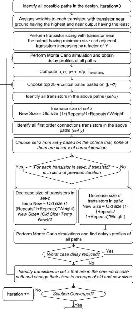
.The LBMP algorithm proposed for transistor sizing of dynamic CMOS circuits while considering process variations is depicted in Fig. 3. As shown in Fig. 1, discharge time of transistors near Gnd is longer compared to the transistors near outputs, as transistors near Gnd are usually driven by many paths. Therefore, path delay is optimized by increasing the size of transistors near Gnd the most and the size of transistors near outputs the least.
As increasing the size of transistor that appears in the most number of paths reduces delays of most paths, the number of paths a transistor is present in is computed and denoted as “repeats”. The initial step in LBMP algorithm is to size adjacent transistors on every path with a fixed size ratio, e.g., 1.1, for optimization convergence. Thereafter, a weight is assigned to each transistor with the one near Gnd having the highest value and the one near the output having the least value. Once the repeats and the weights of all transistors are computed, Monte Carlo simulations while considering process variation are performed to obtain delay profiles of each path. The transistors on the top 20% critical paths are grouped to
set-x, and their sizes are increased and calculated by (3).
As delay of the critical path is dependent on the capacitive load of channel-connected transistors, reducing this capacitive load reduces the overall delay. The 1st order connection transistors in the set-x are identified and grouped to set-y. Then, transistors in set-y that are not in
set-x of the current iteration are grouped to set-z. For
each transistor in set-z, it is checked if the transistor is present in set-x of previous iteration. If so, its size is decreased and calculated by (4) and (5). If not, its size is decreased and calculated by (6).
¸ ¸ ¹ · ¨
¨ © §
u ¸¸ ¹ · ¨¨
© §
u Weight
Repeats 1
Repeats Size
Old Size
New_ _ 1 (3)
¸ ¸ ¹ · ¨
¨ © §
u ¸¸ ¹ · ¨¨
© §
Weight
Repeats 1
Repeats Size
Old New
Temp _ 1 (4)
2 _
_size Old Size TempNew
New (5)
¸ ¸ ¹ · ¨
¨ © §
u ¸¸ ¹ · ¨¨
© §
u Weight
Repeats 1
Repeats Size
Old Size
New_ _ 1 (6)
Once new transistor sizes are determined, Monte Carlo simulations are performed to identify the new top 20% critical paths. If the new worst-case path delay is higher than the delay in the previous iteration, sizes of transistors in set-z of the new worst-case path are changed to the average of old and new sizes. Iterations are repeated until the solution converges to an optimum.
IV. TIMING OPTIMIZATION OF 2-BWEIGHTED BTC Fig. 1 depicts a 2-b Weighted Binary-to-Thermometric Converter (WBTC) used in parallel adders [24]. The 2-b WBTC has two 2-b inputs, (a1 a0) and (b1 b0) and of each
the LSB a0 and b0has a unity weight and the MSB a1and
b1 has a weight of two. The 6-b thermometric output can
represent any number from 0 to 6. This design adds two 2-b binary values and generates a thermometric output and of which the number of ‘1’ equals to its binary input. For an input, (a1 a0) = (1 0) and (b1 b0) = (0 1), the output
is (c5 c4 c3 c2 c1 c0) = (0 0 0 1 1 1). The 2-b WBTC is
TABLE I. TIMING PATHS IN 2-BWBTC
Path
No. Transistors
Path
No. Transistors
1 T28, T0, T4, T11, T22, T26 18 T28, T7, T8, T12, T18
2 T28, T7, T11, T22, T26 19 T28, T7, T11, T15, T18
3 T28, T19, T22, T26 20 T28, T7, T11, T17, T21
4 T28, T24, T26 21 T28, T7, T11, T20, T21
5 T28, T0, T4, T11, T17, T23 22 T28, T14, T15, T18
6 T28, T0, T4, T11, T20, T23 23 T28, T14, T17, T21
7 T28, T0, T4, T11, T22, T25 24 T28, T19, T20, T21
8 T28, T7, T11, T17, T23 25 T28, T0, T1, T5, T13
9 T28, T7, T11, T20, T23 26 T28, T0, T4, T11, T15, T16
10 T28, T7, T11, T22, T25 27 T28, T7, T8, T9, T13
11 T28, T14, T17, T23 28 T28, T7, T8, T12, T16
12 T28, T19, T20, T23 29 T28, T7, T11, T15, T16
13 T28, T19, T22, T25 30 T28, T14, T15, T16
14 T28, T24, T25 31 T28, T0, T1, T2, T6
15 T28, T0, T4, T11, T15, T18 32 T28, T0, T1, T5, T10
16 T28, T0, T4, T11, T17, T21 33 T28, T7, T8, T9, T10
17 T28, T0, T4, T11, T20, T21 34 T28, T0, T1, T2, T3
TABLE II. REPEAT AND WEIGHT OF TRANSISTORS IN 2-BWBTC
Rep-eats
Near Gnd
Near Output
16 T11
12 T0,T7
8 T4
6 T17,
T22 T15, T20 T23 T21
4 T1, T8, T14, T19
2 T5,
T12
T2, T9, T24
T13 T10
1 T6 T3, T27
Wei-
ghts 0.5 0.4 0.3 0.2 0.15 0.1 0.05
The 34 timing paths in 2-b WBTC are presented in Table I. The transistor repeat and weight profiles are shown in Table II. Using minimum size transistors, the worst-case delay of 2-b WBTC was 355 ps from path-1. Sizes of all transistors are initially increased by a ratio of 1.1 and simulations are performed to identify the critical paths. The top 20% critical paths are path-1, 2, 5, 8, 26, and 29. The set-x transistors and their initial sizes on these critical paths are T0 (311 nm), T4 (283 nm), T7 (311
nm), T11 (283 nm), T15 (212 nm), T16 (176 nm), T17 (234
nm), T22 (234 nm), T23 (193 nm), and T26 (193 nm). With
these set-x transistors identified, based on repeat and weight profiles of transistors in 2-b WBTC as shown in Table II, these set-x transistor sizes are increased by (3) to T0 (454 nm), T4 (383 nm), T7 (454 nm), T11 (389 nm), T15
(239 nm), T16 (183 nm), T17 (274 nm), T22 (274 nm), T23
(209 nm), and T26 (208 nm). The 1st order connection
transistors of set-x that are not in the top 20% critical paths are grouped to set-z. They are T1(257 nm), T8(257
TABLE III. CRITICAL PATH ORDER IN 2-BWBTC
Min.
size Iter-1 Iter-2 Iter-4 Iter-6 Iter-9 Path
Rank
Path # Path # Path # Path # Path # Path #
1 1 1 1 25 15 25 2 2 2 2 31 19 31 3 5 17 18 3 5 30 4 8 21 17 34 8 34 5 26 15 21 23 26 32 6 29 19 15 24 29 26 7 17 16 19 22 18 29 8 21 20 16 11 22 22 9 15 5 20 30 33 4 10 19 8 25 32 30 24 11 6 26 5 18 1 14 12 9 29 8 1 2 13
13 20 6 26 2 31 5
14 16 9 29 33 11 8 15 7 7 3 5 25 23 16 10 10 33 8 27 33 17 25 18 27 13 34 15 18 18 25 7 27 16 19 19 33 33 10 15 20 11 20 31 3 31 19 17 27 21 27 31 28 4 21 1 22 34 27 34 16 32 2 23 28 32 32 20 23 3 24 32 34 24 12 3 7 25 3 28 6 17 28 10
26 11 24 9 21 4 18
27 30 22 22 26 7 17
28 24 23 23 29 10 21 29 12 30 30 28 24 16 30 22 11 13 7 6 20 31 4 4 11 10 9 28 32 23 12 12 14 13 12 33 13 13 4 6 12 6 34 14 14 14 9 14 9
Delay
(ps) 355 244 185 170 166 157
nm), T12 (234 nm), T13 (193 nm), T14 (257 nm), T18 (193
nm), T19 (257 nm), T20 (212 nm), T21 (176 nm), T24 (212
nm), T25 (176 nm), and T27 (176 nm). Based on the repeat
and weight profiles of each transistor from Table II, these transistor sizes are reduced by (4) to T1(195 nm), T8(195
nm), T12 (202 nm), T13 (180 nm), T14 (195 nm), T18 (177
nm), T19 (195 nm), T20 (184 nm), T21 (168 nm), T24 (190
nm), T25 (168 nm), and T27 (171 nm). After the transistor
sizing is complete, Monte Carlo simulations are performed to obtain the new critical path order.
The critical path order profile over a few iterations is shown in Table III. With minimum size transistors, the worst-case path is path-1. After the first iteration of LBMP algorithm, its delay is reduced from 355 ps to 244 ps. However, path-17 of which the transistor (T20, T21)
Table IV shows the 2-b WBTC delay convergence profile over 10 iterations. The first column represents the iteration number, the second column represents the worst-case critical path number based on the delay of ȝ + ı, the third column represents the minimum delay of the worst-case path due to process variations, the fourth column represents the maximum delay of the worst-case path due to process variations, and the fifth column represents the delay
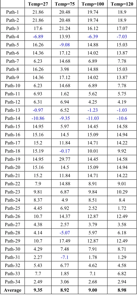
PV of the worst-case path.Efficiency of the LBMP algorithm is illustrated through reduction in delay sensitivity as shown in (2). Table V lists the percentage reduction in delay sensitivity at four different temperatures from 27 oC to 120 oC. Table V shows that although delay sensitivity has reduced in majority of the paths, it has also slightly increased for some paths (4, 5, 13 14, 18, 28 and 31). The ranks of these paths based on their delays are shown in Table VI. The increase in delay sensitivity of these paths is very much acceptable as most of the paths except path-31 do not fall in the set of critical paths.
A comparison of applying the LBMP algorithm to a 2-b WBTC with and without consideration of process variation during the timing optimization is shown in the Table VII. The 2-b WBTC designed without considering process variations has the delay of 161.37 ps [24], while occupying an area of 2.054 ȝm2. By accounting for process variations, the delay was reduced from 161.37 ps to 144 ps, and area occupied reduced from 2.054 ȝm2 to 1.695 ȝm2. This accounts for 10.8% of delay improvement and 17.4% of area improvement.
V. LBMP FOR 4-BUNITY WEIGHT BINARY-TO-THERMOMETRIC CONVERTER
Another circuit used to validate the LBMP algorithm is the 4-b Unity Weight BTC (UWBTC) used in digital-to-analog-converters as shown in Fig. 4. The UWBTC takes a 4-b binary input and generates a thermometric output and of which the number of ‘1’ equals to its binary input. For example, for a binary input (b3 b2 b1 b0) = (0 1 0 1),
the 4-b UWBTC generates an output (c14 c13 c12 c11 c10 c9
c8 c7 c6 c5 c4 c3 c2 c1 c0) = (0 0 0 0 0 0 0 0 0 1 1 1 1 1 1).
Along with the increase in the number of transistors in this 4-b UWBTC, the number of timing paths has also increased to 83. With minimum size transistors, the worst-case delay of the 4-b UWBTC was 152 ps.
After the first iteration of the LBMP algorithm, the worst-case delay reduced from 152 ps to 114 ps. Repeated iterations of the algorithm has reduced its delay to 103 ps, which accounts for 32.23% delay improvement. Table VIII shows the delay convergence profile of the 4-b UWBTC demonstrating that LBMP algorithm works effectively for complex designs with large number of timing paths.
TABLE IV. 2-BWBTC DELAY CONVERGENCE PROFILE
Iteration Critical Path
Min Delay (ps)
Max Delay (ps)
ȝ + ı (ps)
0 1 178 290 355
1 1 156 236 244
2 3 131 215 185
3 25 124 201 171
4 19 119 195 170
5 25 121 193 166
6 21 126 191 166
7 25 119 186 161
8 8 119 176 157
9 25 117 179 157
TABLE V. PERCENTAGE OF DELAY SENSITIVITY (V/P)
REDUCTION IN 2-BWBTC PATHS AT DIFFERENT TEMPERATURES
Temp=27 Temp=75 Temp=100 Temp=120
Path-1 21.86 20.48 19.74 18.9
Path-2 21.86 20.48 19.74 18.9
Path-3 17.6 21.24 16.12 17.07
Path-4 -6.89 13.93 -6.39 -7.03
Path-5 16.26 -9.08 14.88 15.03
Path-6 14.36 17.12 14.02 13.87
Path-7 6.23 14.68 6.89 7.78
Path-8 16.26 3.98 14.88 15.03
Path-9 14.36 17.12 14.02 13.87
Path-10 6.23 14.68 6.89 7.78
Path-11 6.93 1.62 5.62 5.75
Path-12 6.31 6.94 4.25 4.19
Path-13 -0.97 6.52 -1.23 -1.03
Path-14 -10.86 -9.35 -11.03 -10.6
Path-15 14.95 5.97 14.45 14.58
Path-16 15.16 14.5 15.09 14.94
Path-17 15.2 11.84 14.71 14.22
Path-18 15.19 -0.17 10.01 9.92
Path-19 14.95 29.77 14.45 14.58
Path-20 15.16 14.5 15.09 14.94
Path-21 15.2 11.84 14.71 14.22
Path-22 7.9 14.88 8.91 9.01
Path-23 9.81 6.87 9.84 10.29
Path-24 8.37 4.9 8.51 8.4
Path-25 4.45 6.92 2.52 1.72
Path-26 10.7 14.37 12.87 12.49
Path-27 4.38 2.57 3.79 3.58
Path-28 4.14 -5.07 5.97 6.18
Path-29 10.7 17.49 12.87 12.49
Path-30 4.29 7.48 7.91 8.71
Path-31 2.27 -7.1 1.78 1.29
Path-32 5.43 6.77 4.62 4.58
Path-33 7.7 1.85 7.1 6.82
Path-34 2.49 3.06 2.68 2.94
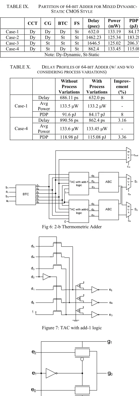
VI. LBMP FOR A MIXED DYNAMIC-STATIC ADDER An optimal balance of delay and power can be achieved by partitioning the design to a mixed dynamic-static circuit style [3]. A 64-b adder architecture used as a test case for timing optimization is shown in Fig. 5, and is divided into two blocks operating in parallel for performance in timing [24]. Block-1 comprises of a 64-b Carry Convergent Tree (CCT) and a Carry Generator (CG) and block-2 comprises of eight 8-b carry-select adders. Each 8-b carry select adder comprises of four 2-b Thermometric Adders (TA) as shown in Fig. 6. Block-1 of 64-b adder computes the seven intermediate carry outputs (C8, C16, C24, C32, C40, C48, C56) which are the
select lines of carry-select adders in block-2. Upon receiving the intermediate carry inputs from block-1, block-2 selects the corresponding pre-computed partial sum as the end result. The 2-b TA consists of an improved Binary to Thermometric Converter (BTC) [11] and a Final Sum (FS) block. The FS block is comprised of a Thermometric-to-Abacus Converter with add-1 logic (Fig. 7), a Thermometric-to-Abacus Converter with add-0 logic, two Abacus-to-Binary Converters (Fig. 8), and multiplexers.
Figure 4: 4-b Unity Weight Binary-to-Thermometric Converter
TABLE VI. 2-BWBTC PATH RANKS AT DIFFERENT ITERATIONS AND TEMPERATURES
Temp=27 Temp=75 Temp=100 Temp=120
Iter-1
Iter-10
Iter-1
Iter-10
Iter-1
Iter-10
Iter-1
Iter-10
Path-4 23 8 24 9 25 10 25 10
Path-5 5 12 5 15 5 16 5 17
Path-13 25 11 25 10 24 9 24 9
Path-14 26 10 26 11 26 11 26 13
Path-18 9 21 9 22 9 4 9 4
Path-28 17 24 17 24 17 23 17 23
Path-31 13 2 13 2 13 2 14 2
Ratio did not decrease Ratio decreased and path became critical
TABLE VII. LBMP IMPLEMENTATION ON 2-BWBTC
w/o Process Variations
w/ Process Variations
Improvement (%)
Delay 161.37 ps 144 ps 10.8
Senstivity 7.87 % 7.4 % 6.0
Area 2.054 ȝm2 1.695 ȝm2 17.4 Average
Power 16.9 ȝW 16.4 ȝW 3.0
TABLE VIII. 4-BUWBTC DELAY CONVERGENCE PROFILE
Iteration Critical Path
ȝ + ı (ps)
Tuncertainty
(ps)
0 28 152 75
1 36 114 27
2 28 111 28
3 27 110 34
4 51 109 29
5 52 107 42
6 58 103 28
7 35 103 27
8 35 104 28
9 35 103 28
10 35 103 27.3
Improvement (%) 32.23 63.6
power is 133.45 mw. However, delay increased from 632 to 862.4 ps, which accounts for a 36.45% increase.
A comparison of applying the LBMP algorithm to the CCT blocks and BTC of the 64-b adder with and without consideration of process variation in the timing optimization is shown in Table X. When the CCT block and BTC are optimized without considering process variations, the worst-case delay of 64-b adder in case-1 was 686 ps. Considering process variations in LBMP resulted in further reduction of delay from 686 ps to 632 ps, and power delay product from 91.6 pJ to 84.17 pJ, which accounts for an 8% improvement in both delay and power delay product. Similarly, accounting for process variations resulted in the worst-case delay of 64-b adder in case-4 to reduce from 890.56 ps to 862.4 ps, and power delay product reduced from 118.98 pJ to 115.08 pJ, which accounts for a 3.16% improvement in delay and a 3.36% improvement in power delay product.
VII. CONCLUSION
In this paper, it is shown that the importance and complexity in timing optimization of dynamic CMOS circuits increases as the number of timing paths and the number and magnitude of process variation increases. A solution addressing these issues is presented through a process variation aware transistor sizing algorithm for dynamic CMOS circuits while considering the load balance of multiple paths in a design.
A 2-b weighted binary-to-thermometric converter was first analyzed, and the worst-case delay was reduced from 355 ps to 157 ps while accounting for 55.77% delay improvement. In addition to reducing the worst-case path delay, it was shown that the proposed LBMP algorithm also reduces the sensitivity and uncertainty due to process variations. A 4-b unity weight binary-to-thermometric converter used in digital-to-analog converters was also analyzed, and the worst-case path delay was reduced through the LBMP algorithm from 152 ps to 103 ps, while accounting for 32.23% delay improvement. Furthermore, through implementation on a 64-b parallel binary adder and partitioning the design to a mixed dynamic-static CMOS logic, the critical path delay was optimized to 632 ps and the power delay product was optimized to 84.17 pJ.
Fig 5: 64-b Adder Block Diagram
TABLE IX. PARTITION OF 64-BITADDER FOR MIXED DYNAMIC -STATIC CMOS STYLE
CCT CG BTC FS Delay (psec)
Power (mW)
PDP (pJ)
Case-1 Dy Dy Dy St 632.0 133.19 84.17 Case-2 Dy Dy St St 1462.23 125.34 183.28 Case-3 Dy St St St 1646.5 125.02 206.37 Case-4 Dy St Dy St 862.4 133.45 115.08
Note: Dy-Dynamic, St-Static
TABLE X. DELAY PROFILES OF 64-BITADDER (W/ AND W/O CONSIDERING PROCESS VARIATIONS)
Without Process Variations
With Process Variations
Improv-ement
(%)
Delay 686.11 ps 632.0 ps 8 Avg
Power 133.5 ȝW 133.2 ȝW - Case-1
PDP 91.6 pJ 84.17 pJ 8 Delay 890.56 ps 862.4 ps 3.16
Avg
Power 133.6 ȝW 133.45 ȝW - Case-4
PDP 118.98 pJ 115.08 pJ 3.36
Fig 6: 2-b Thermometric Adder
Figure 7: TAC with add-1 logic
REFERENCES
[1] D. H. Allen, S. H. Dhong, H. P. Hofstee, J. Leenstra, K. J. Nowka, D. L. Stasiak, and D. F.Wendel, “Custom Circuit Design as a Driver of Microprocessor Performance,” IBM Journal of Research and Development, vol. 44, no. 6, pp. 799-822, Nov 2000.
[2] P. E. Gronowski, W. J. Bowhill, R. P. Preston, M. K. Gowan, and R. L. Allmon, "High-Performance Microprocessor Design," IEEE J. Solid-State Circuits, vol. 33, no. 5, pp. 676 – 686, May 1998.
[3] M. Zhao and S. S. Sapatnekar, “Timing-driven Partitioning and Timing Optimization of Mixed Static-Domino Implementations,” IEEE Trans. CAD of Integrated Circuits and Systems, vol. 19, no. 11, pp. 1322 – 1336, Nov 2000. [4] J. P. Fishburn, and A. E. Dunlop, “TILOS: A Posynomial
Programming Approach to Transistor Sizing,” International Conf. Computer Aided Design, pp. 326-328, 1985.
[5] V. Sundararajan. S. S. Sapatnekar, and K. K. Parhi, “Fast and Exact Transistor Sizing Based on Iterative Relaxation,” IEEE Trans. CAD, vol. 21, no. 5, pp. 568-581, May 2002.
[6] M. Borah, R. M. Owens, and M. J. Irwin, “Transistor Sizing for Minimizing Power consumption of CMOS Circuits under Delay Constraint,” International Symposium on Low Power Design, pp.167-172, 1995. [7] S-O. Jung, K-W. Kim, and S-M. Kang, “Transistor Sizing
for Reliable domino Logic Design in Dual Threshold Voltage Technologies,” GLSVLSI, pp. 133-138, 2001. [8] Z. Luo, “General Transistor-Level Methodology on VLSI
Low-Power Design,” GLSVLSI, pp. 115-118, 2006. [9] A. R. Conn, I. M. Elfadel, W. W. Molzen, Jr., P. R.
O'Brien, P. N. Strenski, C. Visweswariah, and C. B. Whan, "Gradient-based Optimization of Custom Circuits Using a Static-Timing Formulation," Design Automation Conference, pp. 452-459, Jun 1999.
[10] B. Fu, Q. Yu, and P. Ampadu, “Energy-Delay Minimization in Nanoscale Domino Logic,” GLSVLSI, pp. 316-319, 2006.
[11] F. Maloberti, and C. Gang, “Performing Arithmetic Functions Using Chinese Abacus Approach,” IEEE Trans. Circuits and Systems-II, vol. 46, no.12, pp. 1512-1515, Dec 1999.
[12] K. A. Bowman, S. G. Duvall, and J. D. Meindl, “Impact of die-to-die and within-die parameter fluctuations on the maximum clock frequency distribution for gigascale integration,”IEEE J. Solid-State Circuits, vol. 37, no. 2, pp. 183-190, Feb 2002.
[13] P. S. Zuchowski, P. A. Habitz , J. D. Hayes, J. H. Oppold, “Process and Environmental Variation Impacts on ASIC Timing,” IEEE/ACM International Conference on Computer Aided Design, pp.336-342, Nov 2004.
[14] M. Orshansky, “Increasing Circuit Performance through Statistical Design Techniques,” Closing the Gap Between ASIC & Custom, Kluwer Academic Publishers, 2003. [15] D. Burnett, K. Erington, C. Subramanian, K. Baker,
“Implications of fundamental threshold voltage variations for high-density SRAM and logic circuits,” Symposium on VLSI Technology, pp. 15-16, Jun 1994.
[16] K. Takeuchi, T. Tatsumi, and A. Furukawa, “Channel engineering for the reduction of random-dopant-placement-induced threshold voltage fluctuations,” International Electron Devices Meeting, Digest of Technical Papers, 1997
[17] S. Borkar, T. Karnik, S. Narendra, J. Tschanz, A. Keshavarzi, V. De, “Parameter Variations and Impact on
Circuits and Microarchitecture,” Design Automation Conference, June 2003.
[18] C.H. Kim, K. Roy, S. Hsu, R. Krishnamurthy, S. Borkar, “A process variation compensating technique with an on-die leakage current sensor for nanometer scale dynamic circuits,” IEEE Trans. VLSI Systems, vol. 14, no. 6, pp. 646-649, June 2006.
[19] J. Tschanz, K. Bowman, V. De, “Variation-tolerant circuits: circuit solutions and techniques,” Design Automation Conference, pp. 762-763, 2005
[20] C. Piguet, “Low-Power Electronics Design”, CRC Press, 2004.
[21] L. Scheffer, “The Count of Monte Carlo”, ACM/IEEE TAU Workshop, Feb 2004.
[22] J. A. G. Jess, K. Kalafala, S. R. Naidu, R. H. J. M. Otten, and C. Visweswariah, “Statistical timing for parametric yield prediction of digital integrated circuits”, Design Automation Conference, pp. 932-937, 2003.
[23] G. Jensen, B. Lund, T. A. Fjeldly, and M. Shur, “Monte Carlo Simulation of Semiconductor Devices”, Computer Physics Communications, vol. 67, Issue 1, pp. 1-61, Aug 1991.
[24] K. Yelamarthi and C-I. H. Chen, “Transistor Sizing for Load Balance of Multiple Paths in Dynamic CMOS for Timing Optimization,” IEEE/ACM International Symposium on Quality Electronic Design, pp. 426-431, Mar 2007.
Kumar Yelamarthi received his B.E degree from University of Madras, India in 2000 and M.S degree from Wright State University in 2004. Currently, he is working towards the Ph.D. degree in the Department of Electrical Engineering at Wright State University. His research focus is timing analysis and optimization, computer aided design, low-power design, VLSI design flow, arithmetic circuits, and engineering education. He has served as a technical reviewer for several IEEE international conferences and has published over 30 papers in both technical and educational fields. He is a member of Tau Beta Pi engineering honor society, and Omicron Delta Kappa national leadership honor society.