RARE EARTH DOPING OF SILICON
Jasmine Pradissitto
Department of Electrical and Electronic Engineering, University College, London
A thesis submitted to University College, University of London for the degree of Doctor of Philosophy
All rights reserved
INFORMATION TO ALL USERS
The quality of this reproduction is dependent upon the quality of the copy submitted.
In the unlikely event that the author did not send a complete manuscript and there are missing pages, these will be noted. Also, if material had to be removed,
a note will indicate the deletion.
uest.
ProQuest 10042907
Published by ProQuest LLC(2016). Copyright of the Dissertation is held by the Author.
All rights reserved.
This work is protected against unauthorized copying under Title 17, United States Code. Microform Edition © ProQuest LLC.
ProQuest LLC
789 East Eisenhower Parkway P.O. Box 1346
" The highest reward for a person's toil is not what they get for it, but what they become by it."
Glasses have long been successfully doped with erbium ions for amplification at 1.53|im. There is also, however, great interest in doping silicon with erbium for the purpose of integration of optical and electronic devices. However, from the work carried out to date, it is clear that the erbium ion does not interact significantly with the host. This implies that the emission cross-section therefore remains unchanged at approximately lO’^l cm^ resulting in a small gain coefficient in comparison to gains obtained from band to band transitions in III-V's. Thus, if doped material is to provide significant gain and be electrically activated, either the emission cross-section of the ion must be increased or the concentration of active erbium ions be in excess of 1Q20 ions/cm^. An enhancement of the emission cross-section may be achieved by increasing the degree of mixing between the 4 / and 5d levels and electrical activation becomes feasible if the erbium ion is forced into a 'mixed valence' state.
This thesis presents the results of an investigation into the possibility of increasing the radiative cross-section (and therefore, the electrical activation efficiency) in erbium doped silicon. The energy levels of the isolated erbium ion have been theoretically predicted by employing the Thomas-Fermi method. The behaviour of these levels in silicon was then investigated using a Kronig-Penney approach. The results show that fluorine, in addition to erbium in silicon, doubles the radiative cross-section of the rare earth ion by enhancing the mixing of the 4 f and 5d
levels of erbium.
Acknowledgements
For the financial support of this project I would like to thank:
Prof. William Stewart from GEC-Marconi Materials Technology Ltd., Caswell.
The Optical Interdisciplinary Research Council (CIRC).
The Engineering and Physical Sciences Research Council (EPSRC).
I am particularly grateful to Dott. M arco Federighi and Prof. Chris Pitt for their supervision and also their encouragement at the times when it was most needed.
To Dr. Bill Gillin go my thanks for all his practical and verbal assistance, his endless good will and the use of his optical laboratory at the University of Surrey when I was stranded.
A special mention must go to my colleagues at UCL who went before me and who helped me see the wood for the trees: Mr. Andrew James for all his help at the start of the project: Dr. liana Massarek for many an interesting conversation; Dr. Tony Kenyon who also assisted me with the preliminary optical measurements and my thanks to Mr. Fred Stride and Mr. David Prescott for their help in the cleanroom and all their practical advice. I would also like to thank Mrs. Mavis Small for all her encouragement.
The following people have contributed to the fabrication and analysis of the material used during this project:
Dr. Mike Wilson and Dr. Chris Jeynes at the University of Surrey for implantation .
Dr. Odowoly for use of his equipment at Queen Mary and Westfield College.
Dr. Alison Chew of Loughborough Consultants for the SIMS measurements.
reading this thesis, and to Dr. Heng Tan for the loan of his printer over the last year.
Table of contents
Chapter l:Erbium doped silicon base opto electronics
Abstract
^
Acknowledgements
4
Table of contents
6
List of illustrations
11
List of tables
15
16
Abstract 16
Introduction 17
1.1 General Introduction 17
1.2 Rare earths in silicon 18
1.3 Erbium in silicon 19
1.4 Mixed valence 21
1.5 The reduction of Er^"*" to Er^+ 22
1.6 Possible device applications 22
1.6.1 The emission cross-section and gain 24
1.7 Fabrication methods for silicon 26
1.7.1 Ion implantation 26
1.7.2 Other methods 27
1.7.3 Conclusions 27
1.8 The effects of co-dopants 28
1.8.1 Fluorine co-doping 30
1.8.2 Oxygen doping 31
1.8.3 SIPOS 32
1.8.4 Solid Phase Epitaxy (SPE) 33
1.9 Summary 33
1.10 Thesis outline 34
References 37
Chapter 2: Properties of the rare earths
39Abstract 39
2.2 Energy levels of erbium
2.2.1 Pump wavelengths 44
2.3 Stark Splittings 45
2.4 Radiative transitions 45
2.5 Nonradiative transitions 47
2.6 Line broadening mechanisms 47
2.7 lon-ion interactions 48
2.8 Level mixing and co-doping 49
2.8.1 An introduction to the modelling in Chapters 3 and 4 50
Conclusion 51
References 52
Chapter 3: Theoretical modelling of emission cross-sections
53Abstract 53
Introduction 54
3.1 Summary of the steps in the modelling 55
3.2 The isolated erbium atom 57
3.3 The radial wave function 59
3.4 The Thomas-Fermi theory 59
3.4.1 Use of the Thomas-Fermi equation 61
3.4.1.1 Results 62
3.5 Calculation of the radial wave function 63
3.5.1 Results 65
3.6 The angular wave functions 65
3.6.1 The angular wave functions for the erbium ion 65
3.6.2 The application for L-S coupling to the 4/levels of the erbium ion 66
3.7 The erbium atom in a complex 66
3.8 The angular wave functions for the atom in a complex 67
3.8.1 Group theory 67
3.8.2 Results 68
3.9 Calculation of the crystal potential 69
3.9.1 Impurity states in semiconductors 69
3.9.2 Calculation of the silicon crystal potential 70
3.11 Generation of spectra 3.11.1 Introduction
3.11.2 Calculation of the emission cross-section 73
3.11.3 The selection rules 74
3.11.4 Generation of spectral plots 7 5
3.12 Results 76
Conclusion 79
References 81
Chapter 4: The effect of co-dopants on the erbium ion
82Abstract 82
Introduction 83
The model 84
4.1 Mixed valence 85
4.1.1 Pressure and co-doping 90
4.1.2 Level crossing 91
4.2 The band structure of atoms 92
4.2.1 The single quantum well 93
4.3 Parity 96
4.4 Results 97
4.4.1 Eigenvalue solutions with the corresponding Radial wave functions 97 4.4.2 The emission cross-sections and energy levels for co-doped erbium 100
4.4.3 Mixing 102
Conclusion 103
References 105
Chapter 5: Material fabrication and analysis techniques
106
Abstract 106
Introduction 107
5.1 Material fabrication 108
5.2 Ion implantation 109
5.2.1 The MeV ion implanter 109
5.2.2 Ion distribution 110
5.2.5 Annealing
5.2.6 Solid Phase Epitaxy (SPE) 1
5.3 Thermal diffusion ^ ^ ^
5.4 Compositional analysis 11 ^
5.4.1 Secondary ion mass spectrometry 113
5.5 Optical characterisation 114
5.5.1 Fluorescence spectrometer 114
5.5.2 Fluorescence lifetimes 116
Conclusion 116
References 117
Chapter 6: Experimental results
iis
Abstract 118
Introduction 119
6.1 Sample implantation parameters 120
6.2 The effect of fluorine 121
Introduction 121
6.2.1 M ethod 121
6.2.2 Results 122
6.2.2.1 Photoluminescence spectra 122
6.2.2.2 SIMS profiles 127
6.3 Temperature and pump power dependencies 129
Introduction 129
6.3.1 T emperature dependence 129
Method 129
6.3.1.1 Results 129
6.3.2 Pump dependence 131
6.3.2.1 Results 131
6.4 Post-amorphisation and solid phase epitaxial regrowth 134
6.4.1 M ethod 134
6.4.1.1 Results 135
6.4.1.2 Discussion 138
6.5 Thermal diffusion of erbium into silicon 139
Introduction 139
6.5.1 Experimental details 139
6.6 Summary and discussion
6.6.1 Possible excitation mechanisms 143
Conclusion
References 14^
Chapter 7: Conclusions
1487.1 Objectives 148
7.2 Summary of research 149
7.3 Applications 151
7.4 Future work 152
7.5 Final conclusion 153
References 155
Appendix One: Derivation of the Thomas-Fermi equation
156Appendix Two: Simplification of the radial wave function
160Chapter 1
Figure 1.1.1 The energy bands of silicon. 18
Figure 1.2.1 The photoluminescence spectrum of a sample of erbium doped silicon annealed at 900°C for 30 minutes. The inset diagram illustrates the relevant manifold
for the peak transition (1) seen in the spectrum. 19
Figure 1.3.1 A schematic diagram o f the change in the isolated erbium ion's electronic states and emission cross-sections due to the host and a co-dopant. 20 Figure 1.4.1 A schematic diagram of the silicon bands indicating where the erbium
manifold would be sited to enable the 1.535pm transition to occur. 21
Figure 1.6.1 An electrically pumped rare earth laser. 24
Figure 1.6.2 A wavelength conversion device. 24
Figure 1.8.1 The effect of co-implantation in CZ and FZ silicon. 29
Figure 1.8.2 Annealing temperature dependence of erbium PL at 4.2K for FZ and
CZ silicon. 29
Figure 1.8.1.1 PL peak intensity vs. anneal temperatures as a function of fluorine
level during heat treatment. 30
Figure 1.8.2.1 Temperature dependence of the PL intensity for both undoped and
oxygen-doped samples. 32
Chapter Two
Figure 2.1.1 The radial wave functions for Ce^+ in units of the Bohr radius, ao. 41
Figure 2.2.1 The energy levels of the isolated Er^+ ion. 43
Figure 2.2.2 Energy levels of Er^+ labelled with Russell-Saunders ^Lj terms. 44 Figure 2.4.1 1500nm stimulated cross-section for different glass typesÜ. 46
Chapter 3
Figure 3.1.1 Flow diagram depicting the steps taken to calculate the Stark splittings
and emission cross-sections. 56
Figure 3.4.1.1.1 Graph of the screening, %, due to inter electronic repulsion vs.
distance from the nucleus for the erbium atom. 62
Figure 3.5.1.1 A plot of the radial wave function against distance for an electron in
Figure 3.8.2.1 A diagram of the Stark splittings for the ground and first excited
states for Er^+ in a site of cubic symmetry. 69
Figure 3.10.1. Stark split levels with calculated transition wavelengths. 72 Figure 3.12.1 Spectrum of Er3+ in silicon with an (10) factor corresponding to
an ionic silicon lattice. 77
Figure 3.12.2 Spectrum of Er^+ in silicon with an A^ factor (0.1) corresponding to a
predominantly ionic silicon lattice. 77
Figure 3.12.3 Spectrum of Er^+ in silicon with an A^ factor (0.01) corresponding to
a predominantly covalent silicon lattice. 78
Figure 3.12.4 PL spectrum o f Er^+ in silicon with an A^ f a c to r (0 .0 1 3 )
corresponding to a covalent silicon lattice. 78
Figure 3.12.5 Measured PL spectrum of Er^+ in siliconH. 79
Chapter 4
Figure 4.1 A schematic breakdown of the steps undertaken in the modelling. 85 Figure 4.1.1 Schematic diagram of the electronic structure for samarium sulphide in
the semiconducting phase. 86
Figure 4.1.2 A Hubbard diagram for the electronic energy levels of mixed valence
rare earths. 87
Figure 4.1.3 The density of states corresponding to 3n f-d hybrid. 88 Figure 4.1.4 A schematic representation of the conduction {5d ) and the 4 / bands
crossing. 89
Figure 4.1.1.1 The structure of the cation-anion spheres in samarium chalcogenides. 91
Figure 4.2.1.1 A one-dimensional periodic square-well potential. 93
Figure 4.4.1.1 The"^/;5/2 ground level and first excited state normalised wave functions for an electron in an isolated erbium well. The depth and diameter o f the well
are 6.25eV and 2Â respectively. 99
Figure 4.4.1.2 The"^/yy/2 ground level and first excited state "^775/2 normalised wave functions for an electron in an erbium well at a distance of 3.05Â from an adjacent
fluorine well. 99
Figure 4.4.2.1 A plot of emission cross-sections vs. the inter-well distance for three sets of double quantum wells. Erbium has been combined with either erbium,
fluorine or ytterbium. 101
Figure 4.4.2.2 A plot of the emission cross-sections(a) vs. the inter-well distance
for the erbium/fluorine double well system. 103
Chapter 5
Figure 5.2.1.1 A schematic diagram of the system for MeV implantation. 109 Figure 5.2.3.1 A graph of the spreads, ranges and doses associated with implants of
a peak concentration of IxlO^^/cm^. I l l
Figure 5.5.1.2 A block diagram of the fluorescence measurement system. 115
Chapter 6
Figure 6.2.2.1.1 A comparison of the PL spectra for im planted «-type silicon
samples. 123
Figure 6.2.2.1.2 A comparison of the PL spectra for im planted p-typ e silicon
samples. 123
Figure 6.2.2.1.3 PL spectra taken at 80K of Er^+ in «, «+, p and intrinsic silicon. 124 Figure 6.2.2.1.4 PL spectra taken at 80K of fluorine doped Er^+ in «, « + , p and
intrinsic silicon. 125
Figure 6.2.2.1.5 PL spectra taken at 80K for two different fluences of fluorine
doped Er^+ in « -type silicon. 126
Figure 6.2.2.1.6 PL spectra taken at 80K for two different fluences of fluorine
doped Er^+ inp-type silicon. 126
Figure 6.2.2.2.1 SIMS profiles of erbium and fluorine in doped and undoped «-type
silicon. This material had not been annealed. 127
Figure 6.2.2.2.2 SIMS profiles of erbium and fluorine for annealed doped and
undoped «-type silicon. 127
Figure 6.3.1.1.1 PL spectra for erbium in IMP INF taken at temperatures from 80K
to 180K. 130
Figure 6.3.1.1.2 A plot of the total integrated PL intensity for the spectra in Fig.
6.3.1.1.1 vs. l/tem perature(l/K ). 130
Figure 6.3.2.1.1 PL spectra taken from the front and back surfaces o f the fluorine
doped «-type sample. 132
Figure 6.3.2.1.2 A plot of pump power vs. total PL intensity. 133
Figure 6.4.1.1.1 Erbium PL spectra taken at 80 K for undoped « and p -ty p e
Figure 6.4.1.1.2 PL spectra taken at 80 K for fluorine doped n and p-type substrates implanted with two different fluences of erbium and fluorine and regrown by SPE.
136 Figure 6.4.1.1.3 PL spectra taken at 80 K for both fluorine doped and undoped
n-type substrates implanted with low concentrations of erbium and fluorine, which have
been subjected to both the single and two step (SPE) anneals. 137
Figure 6.4.1.1.4 PL spectra taken at 80 K for both fluorine doped and undoped
n-type substrates implanted with high concentration of erbium and fluorine which have
been subjected to both the single and two step (SPE) anneal. 137
Figure 6.4.1.1.5 PL spectra taken at 80 K for both fluorine doped and undoped
p-type substrates implanted with high concentrations of erbium and fluorine which have
been subjected to both the single and two step (SPE) anneal. 138
Figure 6.5.2.1.1 SIMS profile for erbium diffused into silicon for a period of 16
hours. 140
Figure 6.5.2.1.2 Photoluminescence spectrum taken at 80K for erbium diffused into
silicon. 141
Chapter 2
Table 2.1 The elements of the lanthanide series. 40
Table 2.2 Emission cross-sections and peak positions for the 1535nm transition in
erbium. 49
Chapter 4
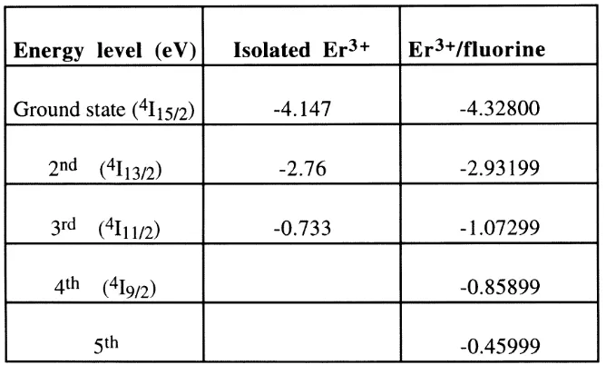
Table 4.1 Calculated eigenvalues for erbium. 98
Chapter 6
Chapter 1: Erbium doped silicon based opto-electronics
Chapter 1:
Erbium doped silicon based opto
electronics
Abstract
Introduction
1.1 General Introduction
Photonic technology may be a driving force for many technological developments in the coming years. The enormous speed and bandwidth may enable, a wealth of sophisticated telecommunication services. Future information highways will also be based on photonic technology. The challenge therefore lies in the integration of both electrical and photonic technologies into one opto-electronic system. This would allow information to be generated, transported, switched and received as light or electrons. Opto-electronics could also lead to revolutionary developments in medicine in the applications of laser surgery, blood sensing and optical imaging.
For the developm ent of this technology new opto-electronic materials are required for the waveguiding, switching, multiplexing and amplification of lighth2. In turn, these com ponents demand light sources operating at the appropriate wavelengths. The dominant material in the microelectronics industry is silicon, and one potential approach to the integration of higher levels of optics and electronics is to combine the different functions on a common silicon substrate.
Silicon has a number of attractive properties as a substrate for integrated optics. It is relatively low in cost and available in large quantities. It has high thermal conductivity and useful electronic properties. Unfortunately, bulk-crystalline silicon exhibits very inefficient light emission due to its indirect energy gap (Fig. 1.1.1). Indeed, the radiative recombination of an electron excited into the conduction band with a hole in the valence band, occurs with an efficiency of less than 10'^; i.e. one photon is em itted per every m illion electrons injected^. Consequently, crystalline silicon has long been considered unsuitable for certain opto electronic applications, and III-V semiconductors have been the preferred materials of use. However, silicon technology, being mature, and the material being both cheap and highly integratable, suggests that silicon may be a more attractive host for lasing ions than glasses and III-V semiconductors.
Chapter 1: Erbium doped silicon based opto-electronics
silicon and from silicon clusters^, while the latter consists mainly of light emission from rare earth doped s i l i c o n 5 , 6 . This thesis will focus upon the latter approach.
conduction band
electrons
holes
valence band
Crystal momentum p
Figure 1.1.1 The energy bands of silicon. The dashed arrow represents the recombination of an electron with a hole and requires a phonon to be supplied before a photonic transition can occur^.
1.2 Rare earths in silicon
The luminescence properties of rare earth ions in solids in the visible and infrared spectral regions were extensively studied in the 1960's and 1970's^. This work was almost entirely concerned with the optical properties of rare earth ions in ionic host crystals such as oxides and halides^’ However, rare earth ions in their 3+ state present an incomplete 4 / shell shielded by the outer 5s and 5p electrons: because of this shielding process, the spectrum which arises from the in tra-^ / transitions is almost entirely independent of the host matrix. In particular, erbium ions emit light from the "^Ii3 /2 to 11 5 /2 transition at about 1.54pm (Fig. 1.2.1). This is the standard wavelength utilised in the communication industry as it falls within the window of minimum loss for optical fibres
M olecular Physics These groups have concentrated upon the fact that the luminescence intensity of the erbium ion increases if part of a complex with other impurity atoms such as oxygen, fluorine, nitrogen and carbon. However, these complexes are little understood in their formation, dissociation and structure.
T=80K
1.500 1.550 1.600
WAVELENGTH (urn)
1.650 1.700
hv=1.535|im
15/2
Figure 1.2.1 The photoluminescence spectrum of a sample of erbium doped silicon annealed at 900°C for 30 minutes The inset diagram illustrates the relevant manifold for the peak transition (1) seen in the spectrum on the left.
1.3 Erbium in silicon
The recombination energy of an electron-hole pair in silicon is sufficient to excite an electron from the ground manifold to the first excited manifold in erbium. Therefore it is energetically possible to excite the erbium ion by carriers injected into silicon in, for example, a p-n diode structure. This was first demonstrated by Ennen
et al. at tem peratures below 77K in 1983^. M ore recently, room tem perature electroluminescence has been demonstrated^^.
Chapter 1: Erbium doped silicon based opto-electronics
ions/cm^. U nfortunately, the latter is difficult to achieve in silicon, because significant lattice damage is likely to occur at higher dopant concentrations^O. In addition, erbium begins to cluster at concentrations greater than 10^^ ions/cm^ and to form erbium silicide (ErztSig)^!. With this limitation on the concentration, the way forward would appear to be to try to increase the radiative cross-section of the ion.
Selection rules forbid electric dipole transitions within the 4 / band, but the radiative cross-section is not zero, for two reasons: 1) the existence of a magnetic dipole interaction and 2) the mixing between the 4 / and 5d energy states. If it were possible to modify the wave function in such a way that this 4 f-5 d mixing was enhanced (Fig. 1.3.1), the result might be to increase the cross-section without a significant alteration in wavelengths of emission and absorption (which are primarily determined by spin-orbit interactions)^9. The same alteration of the wave function may further result in an improved interaction between erbium and the semiconductor host. Thus, the electrical activation of the dopant may be enhanced.
Single. electron
electron__ repulsion
Spin-orbik
coupling Host
7/2
I
a= 0 cm2
Tailoring of
host with
co-dopant?
(f-d mixing)
I
a=10“2icm2 a = 1 0 “‘^cm2
1.4 Mixed valence
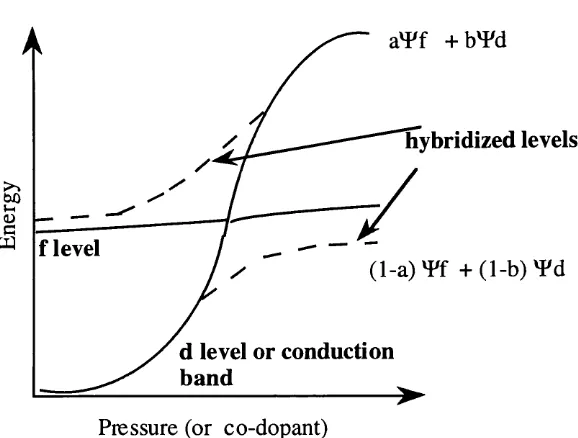
4f-5d mixing has been shown to occur in the rare earths due to their 'mixed valence' p r o p e r t i e s ^ 2 , 2 3 The energy levels may be made to overlap by applying pressure to the material containing the rare earth ions. This pressure can be applied either mechanically or structurally by co-doping with an ion of appropriate size or electronegativity24, in the latter case, the degree of mixing will depend upon both the ionic species and the concentration of ions present. This is equivalent to modifying the distance between the erbium and co-dopant ions.
conduction band electro n s
/
11/2
*13/2
hv=1.535|J.m%
15/2
holesvalence band
Crystal momentum (p)
Figure 1.4.1 A schematic diagram of the silicon bands indicating where the 4/ erbium manifold would be sited to enable the 1.535|i.m transition to occur. Note that in comparison to Fig. 1.1.1, no phonon is required for electron-hole recombination. The Er^+ electronic states provide intermediate levels for electrons to fall into on their way to the valence band. For this to occur, the erbium ion would have to fluctuate between the 2+ and 3+ states.
Chapter 1: Erbium doped silicon based opto-electronics
being reduced to a 2+ ion, Fig 1.4.1). 'Fluctuating' or 'mixed' valence is a property unique to the rare earths and is discussed in detail in Chapter 5.
1.5 The reduction of Er^+ to Er^+
The reduction o f the Er^+ ion to Er^+ has been extensively studied in ionic crystals, including alkaline-earth halides^^. Doping of a salt such as calcium fluoride with an ion that differs from the calcium or fluorine valence by a value of one (i.e. 3+ or 2"), has been used to study crystal imperfections^^. For example, consider oxygen diffusing into calcium fluoride. The necessity for charge neutrality inevitably suggests that an electron trap vacancy (an F centre) will form in the crystal. This is one possible mechanism for maintaining electrical neutrality; another is to change the valence of the dopant ions to match the corresponding ions in the host. Therefore, Er^+ would accept an extra electron to become Er^+. In this case, no charge compensators such as F centres are required.
The different methods of reducing the rare earth ion in alkaline-earth halides include gamma irradiation^^, and solid state electrolysis^^. The latter results in a permanent change of valence and a visible colour change within the sample crystal. Numerous spectra of stable divalent rare earths in ionic crystalline hosts are provided in reference^^. However, all transitions fall within the absorption band of silicon and, for this reason, even if Er^+ ions were present, their identification by means of luminescence would be difficult. In Sec. 1.8, the effect of co-dopants on Er^+ in silicon is addressed. V arious papers suggest that the reason for increased luminescence upon the introduction of electronegative ions, such as fluorine, is due to Er^+ undergoing oxidation to a 3+ state (the reverse o f the process given in the paragraph above). Thus, the fluctuating valence property o f the rare earths is probably already being employed in the luminescence mechanism within silicon. However, due to the enormous problems associated with the identification of the 2+ ion in silicon, it is not addressed further within this thesis.
1.6 Possible device applications
practical terms, with the direct current injection used to power semiconductor-based optical amplifiers and lasers. Clearly, integration with electronic devices on silicon substrates would be much more difficult to realise if optical pumping were the only option. In semiconductors, on the other hand, the optical transitions used for am plification are 'band to band' transitions. These are ideal for w ide band amplification but not for applications in which high spectral purity is a requirement, such as wavelength division multiplexing. Spectral purity can be obtained by using a single-mode semiconductor laser which employs an external cavity, or a distributed- feedback laser (DFB) using an etched diffraction grating^^. If the in tra-4 / shell transitions in rare earths could be combined with the direct electrical pumping offered by semiconductors, then we would have some interesting possibilities for realising spectral purity. Indeed, with all the different rare earths that exist, it becomes possible to have one material em itting light at various different w avelengths depending upon the dopant ions being activated. lon-ion interactions between different dopants could be used to transfer energy from one frequency to another without dissipating it into the phonon structure; an effect already successfully demonstrated in glass hosts (Chapter 2).
There exists very little literature on the nature o f potential device
a p p l i c a t i o n s b u t all the possibilities will have one thing in common: the use of 4 f
shell transitions in place of, or in addition to, inter-band transitions provided by the semiconductor host. Wide band optical amplification is clearly not an objective, but selective amplification of certain wavelengths is. Since semiconductor lasers and am plifiers already exist, use of the rare earths is only justified for reasons of wavelength selection or spectral purity. The following are two suggestions for possible device applications:
1. an electrically pumped rare earth laser (Fig. 1.6.1);
2. a device for wavelength conversion (Fig. 1.6.2);
C hapter 1: Erbium doped silicon based opto electronics
conduction band Current injection
valence band
1535nm
Figure 1.6.1 An electrically pumped rare earth laser. A second upper excited state is precluded as the electrons come directly from the conduction band of the semiconductor. This would also improve the efficiency of the electron-hole recombination in silicon as a phonon would no longer be required for the photonic transition to occur.
conduction band Optical pump
valence band
1535nm
F igure 1.6.2 A wavelength conversion device. In this application, the excitation of the silicon conduction-to-valence band transition is still by optical means. However, the resultant emission is no longer due to the intra-band transitions in the semiconductor. Instead the intermediate atomic rare earth levels dictate the emitted wavelengths. The emission cross-section is unknown.
1.6.1 The emission cross-section and gain
The maximum gain g, at 1535nm (which arises upon a transition from the first excited state (2) to the ground state (1), where 2 and 1 represent bands almost equivalent to discrete energy levels) is defined as
8 = (^2l^a (1.6.1.1)
where Na is the number of active atoms (or ions) and 0 2 1 is known as the emission cross-section and has the dimensions of area i.e. cm^. In addition, the probability
{P2 1), of a transition per second, occurring from the first excited state to the ground level can be shown to be
P ll = <y2\VNa
(1
.6
.1
.2
)where v is the group velocity of the incident photons in the material {P2 1 is also inversely proportional to the lifetime of the transition, x). Thus, for increased gain in the material, either: 1) the emission cross section must increase, which will require an increase in the probability of a transition occurring (hence, x must decrease), or 2) the concentration of erbium ions must be increased. The maximum concentration has been shown to be limited (Sec. 1.3) and therefore it is the former approach which has been investigated in this project. The value of this direction is confirmed by results obtained from m o d e l l i n g ^ ^ which have shown that, even with a concentration of approximately IxlO^Ocm'^, the maximum gain possible (independent of the host material) is of the order of IdBcm k From E q .(l.6.1.1) the gain of different active materials can be calculated and compared to the maximum possible gain from erbium in a silicon host. In III-V materials such as InGaAsP, the gain possible from intra band transitions is 200cm" ^ or 860dB cm "k However, at a concentration of
C hapter 1; Erbium doped silicon based opto-electronics
1.7 Fabrication methods for silicon
Various methods of fabrication have produced optically active erbium doped silicon, e.g. molecular beam epitaxy (MBE) and ion implantation. The following is a brief summary of the experimental conditions under which material has been obtained as described in recent papers. Due to the limited facilities available for this project, ion implantation was the selected method.
1.7.1 Ion implantation
In 19835, it was reported that well-resolved, sharp lum inescence peaks at 1.54|Lim could be observed in erbium implanted silicon if it was prepared in the following manner: ion implanted at 350keV using concentrations of erbium varying from 5x10¹³ to 5xlOT4 ions cm'^. For spectral characterisation, the specimens were cooled to 20K and excited with the 514.5nm or 457.9nm line of an argon ion laser. Similar results were obtained in 1989, when l^^Er was implanted into silicon at 250keVl5 in concentrations between 1x10^3 and lxlQ l5 cm ‘^.
The work conducted in 1983 was the first to draw some conclusions as to the effect of the dopant concentration, the annealing time, and the temperature, upon photolum inescence intensity. It was found that as the ion dose increased, the em ission intensity decreased in the m aterial prepared at the low er annealing temperatures. One suggested explanation for this was that the increased ion dose would cause increased lattice damage. Therefore, the number of sites with tetrahedral (T) symmetry (which corresponds to a substitutional position) would be diminished. The effect of the annealing temperature could be explained by the erbium tending to occupy non-T symmetry sites. These are not thermally stable at lower temperatures. As the temperature is raised, more erbium ions revert to T positions but, if annealed for too long, they begin to diffuse to the surface. Since so few ions are initially in T sites, the implication is that they are in interstitial positions. This paper suggests that the production of material with optimal photoluminescence, requires an anneal at 900°C for a period of 30 minutes, and an incorporated erbium concentration of
pairs, rather than direct optical excitation. This hypothesis was tested by illuminating the sample from the rear face^^. This effectively blocks out the direct excitation beam so that only photo-generated carriers can travel the necessary 500|im, through the sample thickness, to exite the erbium centres. The observed photoluminescence decreased by only 20% compared to the front illum inated case, confirm ing the hypothesis suggested. If photo-generated electron-hole pairs are responsible for the excitation then injected carriers in a p-n diode should have a similar effect^^.
1.7.2 Other methods
Ion im plantation has been the preferred method for m ost o f the groups working in this field, but methods such as molecular beam epitaxy (MBE)^^ and thermal diffusion^^ have also been studied. A few papers describe methods by which rare earths, including erbium, were made to diffuse into silicon. It was found that the rare earths possess diffusion properties similar to those of other group III elements, in that they migrate between crystal lattice sites. In none of these papers, however, was erbium reported to luminesce.
In 19856, erbium doped silicon light emitting diodes (LEDs) were produced by MBE. p-n junctions were formed by growing an erbium doped p-type epitaxial silicon layer onto an «-type silicon substrate. When the diodes were biased in the forward direction, and m easurem ents taken at 77K, sharp electrolum inescence emissions at 1.54|xm were obtained. It appears that the erbium ion may have been excited by (free) carriers within the p-n junction region. The problem remained that the quantum efficiency of the process was found to be merely 5x10"^ at 77K and not observable at room temperature.
1.7.3 Conclusions
Chapter 1; Erbium doped silicon based opto-electronics
process has the effect of not only repairing crystal damage but providing the impurity ions with enough energy to migrate to substitutional positions^^.
1.8 The effects of co-dopants
The effects of impurity co-doping in erbium implanted silicon were first studied in 1991 by J. Michel et a l at AT&T and their paper was the starting point for much of the experimental work conducted during this study 12 (although, at this time, the material fabrication parameters had not yet been optimised). The results of their work demonstrated that emission would only be observed in silicon if the erbium ions formed some kind of complex, mainly with oxygen. They found that unless the silicon used was Czochralski-grown (CZ), in which the concentration of oxygen is of the order of IxlQl^cm"^, the intensity of the emitted fluorescence was significantly lower than in the case of float-zone (FZ)-silicon, in which the oxygen concentration is -Ix lQ l^cm '^ . The AT&T paper also discusses the effects o f co-im plants. A significant variation in the intensity of the erbium emission was observed for different co-implant atoms. The conclusion drawn was that impurities modify the chemical environment around the ion and are essential for the formation of optically active Er^+ centres.
100
6 0
CO c: d)
n
n
20
F Z l
A1 Si P S Cl
Er B C N 0 F
I m p l a n t e d I m p u r i t i e s
F igure 1.8.1 The effect o f co-im plantation in CZ and FZ silicon. The peak concentration o f all the
elem ents was 1x10^^/cc. A ll the sam ples were annealed at 900°C for 30 mins^^.
C
^ 10'
JD CO
M IQ-
C
(V
10 J L
^ C Z - S i \
\
^ \ A
\
F Z - S i
o
J L
6 0 0 7 0 0 8 0 0 9 0 0 1 0 0 0 1 1 0 0
T e m p e r a t u r e (C)
Figure 1.8.2 A nnealing temperature dependence o f erbium photolum inescence at 4.2K for FZ and CZ
silicon. The peak concentration w as 1x10*^ fee. The FZ data provided is that from sam ples with
additional oxygen implants. The annealing time was 30 m in s’^.
Chapter 1: Erbium doped silicon based opto electronics
1.8.1 Fluorine co-doping
In another very recent paper from the same group at AT&T, fluorine enhanced Er^+ light emission was studied in d e t a i l T h e main conclusion drawn was that the erbium -fluorine com plex is 100 times m ore effective than the erbium -oxygen complex in generating light emission at 1.54)j.m in silicon. The luminescence light intensity was found to be linearly proportional to the total number of retained fluorine atoms in silicon after heat treatment (Fig. 1.8.1.1). It is eventually limited by the damage associated with the higher doses of fluorine implantation. The optimum annealing temperature which achieves the maximum intensity was found to decrease from 1000°C to 800°C (for a 30 minute anneal) as the fluorine im plantation concentration increases. Thus, the silicon/erbium anneal and the optimum processing window are determined by the interaction of three processes occurring during heat treatment: 1) dam age recovery/complex form ation; 2) fluorine out-diffusion; 3) erbium-fluorine complex dissociation.
1 0'
lo '
1 0"
1 0'
Damage
Recovery F G ut-dirT uslon Er-F Complex Dissociation
^ d is . = 2.4 cV
5x10** ► 3x10** O I x l O '*
4x10** A 2x10** A 5x10*7 J ________I________I________I_____
700 800 900 1000 1100
A nnealing T e m p e r a tu r e (C)
Figure 1.8.1.1 Photoluminescence peak intensity vs. anneal temperatures as a function of the fluorine level during the heat treatment process*^.
1.8.2 Oxygen doping
In several p a p e r s ^ 4 , 4 0 , 2 0 luminescence was reported to be stronger in CZ silicon (which contains an average concentration of IxlO^^cm"^ of oxygen centres), than in FZ silicon. Some p a p e r s ^ 4 , 4 0 explored the direct role played by oxygen impurities in the optical activation of the 1.54pm luminescence by implanting oxygen into erbium-doped silicon at concentrations comparable to those of the rare earth.
In a review of the effect of oxygen co-doping^O, it was suggested that the reason for an increase in the luminescence intensity is that erbium behaves as a donor in the presence of oxygen, which therefore has the effect of enhancing the electrically active population by several orders of magnitude. This suggests that the local environment around the erbium ion is changed in the presence of oxygen. This is supported by Extended X-ray Absorption Fine Structure (EXAFS) measurements from erbium implanted CZ-silicon, which reveal a local six fold co-ordination of oxygen atoms around each erbium ion^T By contrast, similar concentrations of erbium in FZ-silicon, which are essentially optically inactive, show that erbium is co ordinated to twelve silicon atoms. This paper also concludes that erbium in silicon behaves as an oxygen getter, only reacting with silicon when either the amount, or the accessibility of oxygen is limited.
The enhancement in both erbium donor behaviour and luminescence in the presence of oxygen suggest that these two quantities may be correlated. The donor levels might be associated with an optically active 3+ state. In addition, a slight shift in the peak of the luminescence spectrum from 1.538pm to 1.534pm suggests that oxygen modifies the local erbium environment. Further experiments showed that the shape of the spectrum is not sensitive to the absolute concentrations of erbium and oxygen, but rather to the erbium/oxygen ratio.
C hapter 1: Erbium doped silicon based opto-electronics
temperature increases, the erbium ion may be losing energy nonradiatively through the crystal (Chapter 6).
Temperature (K)
300250 200 150 100
■ 0 —doped O Undoped
JO
O
CO
c
0)
c
CL
>-2
1 0 0 0 /T (K’ O
Figure 1.8.2.1 Temperature dependence of the photoluminescence intensity for both the undoped (circles) and oxygen-doped (squares) samples'^^.
The co-doping of erbium has also led to recent m easurem ents of room temperature electroluminescence ( E L ) 4 3 . p-n diodes were fabricated and it appears that the electroluminescence intensity increases linearly with the current passing through the device. The limiting steps were suggested to be nonradiative decay processes and limited pumping efficiency.
1.8.3 Semi-insulating polycrystalline silicon
The concept of oxygen doping has been successfully extended to other m aterials such as SIPOS (sem i-insulating polycrystalline silicon), which is a semiconductor fabricated using low-pressure chemical vapour deposition from SiH^ and N2O. This material combines the advantages of silicon as a semiconductor, in which carriers can be generated, and Si0 2, which is a good host for erbium (i.e. can activate a high fraction and is subject to limited temperature quenching). Lombardo
1.8.4 Solid phase epitaxy
In an effort to limit both the number of implantation induced defects and increase the concentrations within silicon without the onset of precipitation, various groups have been w orking on the solid phase epitaxy (SPE) re growth of erbium im planted crystalline silicon (c-Si) which has been post-am orphised in the im planted r e g i o n l 2 , 3 4 , 4 2 , 4 5 , 4 6 Polman et have incorporated erbium in silicon at high co n ce n tra tio n s,-10^®cm~^. This concentration is some two orders of m agnitude higher than previously achieved. If the total amount of erbium incorporated in c- silicon could be optically activated (as opposed to the 1-2% actually activated)^^, the fabrication of silicon based optical devices would become feasible.
1.9 Summary
To summarise, the im portant points that arise from the literature can be separated into two main categories. The first category listed below under headings (1) to (5), addresses the factors affecting the process of Er^+ luminescence in silicon. The second category, listed (6) to (9), involves possible device fabrication and increased electrical activation. The conclusion that is immediately apparent is that firstly, the fraction of optically active centres must be increased from the present 1- 2% and secondly, that all the noted features must be optimised if material of device quality is to be realised. The limiting factors are:
1) erbium must be in the optically active 3+ state;
2) erbium must be incorporated within silicon in concentrations avoiding precipitation i.e. presently at IxlO^^/cc^;
3) the pumping efficiency of the Er^+ sites through electron-hole processes should be as high as possible;
4) the crystalline quality of the silicon host matrix must remain high to avoid alternative nonradiative recombination routes to the electron-hole pairs;
5) the routes for nonradiative de-excitation of the pum ped Er^+ sites should be minimised;
6) m aterials doped with rare earth ions do not exhibit an increase in carrier concentration. The rare earth ions are therefore electrically inactive;
Chapter 1: Erbium doped silicon based opto-electronics
8) the spectra of incorporated ions and their radiative cross-sections are largely unaffected by the host (except for Stark splittings) and are similar to those of the isolated ion (lO'^^cm'^ for the emission cross-section). Hence the gain for silicon doped material is small (less than 6cm'^), which is two orders of magnitude lower than the compound semiconductor counterpart;
9) the sites at which the dopant ions are located are dependent upon the method of fabrication.
1.10 Thesis Outline
From the summary above, the objective of this project was to investigate points (1), (4), (7), and (8). The emission cross section (8) in particular, appears to be one of the most limiting factors. Even with a significant increase in the optically active fraction, the carrier concentration and the material quality, the gain would not be large enough for a lasing material to be feasible (see Sec 1.6.1).
The organisation of this thesis is as follows: C hapter 2 discusses the properties of the rare earths with particular attention to Er^+ and the factors affecting luminescence. In order to study the behaviour of the emission cross-section, a model has been developed of the Er^+ energy levels based upon the Thom as-Ferm i approximation for the radial component of the 4 f wave function, and on symmetry group theory for the angular part of the wave function. This is discussed in Chapter 3. The treatm ent is less rigorous than, for exam ple, the H artree-Fock approach; nevertheless, as we expect to find a large change in the radiative cross-section - and electrical activation energy - the accuracy is adequate for the present purpose. The validity of the model was tested by theoretically calculating fluorescence spectra for Er3+ and com paring to experimental measurements. The ion was situated both interstitially and substitutionally within a silicon host.
Chapter 4, discusses how the above model was expanded to study the effect of co-dopants on the levels of erbium. This was achieved by constructing a two dimensional, quantum well system with the parameters pertaining to the Er^+ ion and a co-dopant such as fluorine. Emission cross-sections calculated from Chapter 3 and 4 show that the presence of fluorine does increase both the level of mixing and the emission cross-section. The concept of 'mixed valence' is also discussed.
The experimental investigation (Chapters 5 and 6) centres upon the use and effect of co-dopants on the luminescence intensity of erbium in silicon. This was investigated for different types of silicon {n, p n+ and intrinsic), to examine the effect that different levels of carriers had on the luminescence. In addition, methods of introducing erbium into silicon in a less destructive manner than ion implantation, were explored, such as thermal diffusion. The first photoluminescence spectrum of doped material created in this manner has been published. Solid phase epitaxial re growth of fluorine doped material has also been carried out in an attempt to decrease emission lost due to nonradiative processes.
Chapter 1: Erbium doped silicon based opto-electronics
References
1. H, Koglenik, Theory o f dielectric waveguides' in 'Integrated Optics', T. Tamir (ed.), Springer-Verlag (1979).
2. R.Soref, IEEE J. o f Quant. Elec., Vol. QE-22, No. 6, (June 1968). 3. F. Priolo et a l. Mat. Res. Soc. Symp. Proc., Vol.
316,
397, (1994). 4. H.A. Atwater et a l. Mat. Res. Soc. Symp. Proc., Vol.316,
(1994). 5. H. Ennen et a l, Appl. Phys. Lett.43,
943, (1983).6. H. Ennen et a l, A p p l Phys. Lett.
46,
381, (1985).7. S.M. Sze, Semiconductor devices, Physics and Technology, Wiley, (1985). 8. R. Reisfeld, Lasers and excited states o f rare earths, (1977).
9. G.S. Ofelt, J. ofC hem. Phys., Vol.
37,
No.3, 511, (1962). 10. B.R. Judd, Phys. Rev. Vol.127,
No.3, 750, (1962). 11. P. Urquhart, lE E Proc.,135,
385, (1988).12. J. Michel, J.L. Benton, R.F. Ferrante, D.C. Jacobson, D.J. Eaglesham, F A. Fitzgerald, Y.H. Xie, J.M. Poate, and L.C. Kimerling, J. A p p l Phys.
70
(5), 2672,(1991).13. F.Y.G. Ren et a l. Mat. Res. Soc. Symp. Proc. Vol
316,
493, (1994). 14. A. Polman et a l. Nue. Inst. A nd Methods in Physics Research , (1992). 15. A. Polman et a l, J. A p p l Phys.77
(3) 1256, (1995).16. Y.S. Tang, K. C. Heasman, W. P. Gillin, and B.J. Sealy, Appl. Phys. Lett.
55
(5), 4 32 (1989).17. B Zheng et a l and D.C. Jacobson and J.M. Poate, A p p l Phys. Lett.
64
(21), 2842,(1994)18. Y. H. Xie et a l, J.Appl Phys. 70, (6), 3223, (1991).
19. W. Miniscalco, Erbium-doped glasses for fibre amplifiers at 1500nm, IEEE J. Lightwave Technol, 9, 2, 234, (1991).
20. F. Priolo, S. Coffa, G. Franzo, C. Spinella, A. Cam era and V. Bellani,
J.Appl.Phys.
74
(8), 4936, (1993).21. D.J. Eaglesham, J. Michel, E. A. Fitzgerald, D.C. Jacobson, J.M. Poate, J.L. Benton, A. Polman, Y.H. Xie and L.C. Kimerling, A p p l Phys. Lett.
48,
2797, (1991).22. R.D. Cowan, Nuc. Inst, and Methods,
110,
173, (1973).Chapter 1: Erbium doped silicon based opto-electronics
28. G.H. Dieke, Spectra and energy levels o f rare earth ions in crystals, Wiley- Interscience, New York, (1968).
29. S.M. Sze, Physics o f Semiconductor Devices, 2"^ ed., Wiley (1981). 30 J. Michel et a l. Mat. Sci. Forum, Vols
143-147,
707, (1994).31. M.A. Lonso and H. Valck, Quantum mechanics. Applications 77 (1981). 32. Private communication from Dott. M.Federighi at UCL.
33. J. Senior, Optical Fibre Communications, Prentice Hall International, (1984). 34. S. Coffa et al, Phys. Rev. B Vol
48,
No.16,
11782, (1993).35. F.Priolo et a l, J. A p p l Phys.
78
(6), 3874, (1995). 36. H. Efeoglu et a l, MRS Proc., Vol220,
(1991).37. D.E. Nazyrov, G.S. Kulikov, and R. Sh. Malkovich Sov. Phys. Semicon.
25(9), 997,(1991)
38. H. Przybylinska et al.. Mats. S c l Forum ,Vols
143-147,
715 (1994). 39. Private communication from Dr. W. Gillin at the University of Surrey. 40. P.N. Favennec et a l, Jap.J. o f A p p l Phys. Vol29,
No.4, L524, (1990). 41. D.L. AdX&v et a l, A p p l Phys. Lett.61
(18) 2181, (1992).Chapter 2:
Properties of the rare earths
Abstract
Chapter 2: Properties of the rare earths
Introduction
This chapter summarises the properties of rare earths both as isolated ions and in the context of a dopant within a host. W here certain properties have not been measured within silicon, examples are given from glass hosts. Glasses have been successfully doped with rare earth ions by a variety o f methods, leading to the developm ent o f optically pumped fibre lasers and amplifiers. One of the most important points discussed is the effect that the host crystal field has upon the shape and magnitude of the emission spectra.
2.1 The rare earths
The rare earths, or lanthanides, form a group of 15 chem ically sim ilar elements occupying the penultimate row of the periodic table T They have an unfilled 4 / shell in common. The name and chemical symbol of the each of the elements in the lanthanide series are shown in Tab.2.1.
Rare-earth Chemical
symbol lanthanum ^^La cerium 58Ce praseodymium 59pr neodymium 60Nd promethium 61pm samarium 62Sm europium 63Eu
gadolinium 64cd terbium 65xb dysprosium 66Dy holmium 67Ho
erbium 68£r thulium 69jm ytterbium 70yb lutetium 21Lu
Table 2.1 The elements of the lanthanide series with their atomic numbers^.
communications. As stated earlier, the 5s and 5p shells shield the 4 f orbitals of the rare earth ions from host lattice effects. Thus, the absorption and emission spectra of the ions are largely unaffected by the host material. Since it is the properties o f the unfilled 4 f shell that are of interest, further discussion is confined to these. Fig.2.1.1 depicts the radial parts of the 5s, 5p and 6s wave functions for Ce3+ and illustrates the extent to which the 4fv/av& functions lie within the closed 5s^5p^ shelP.
1
UJ o 3
1-0
2
<
■1
1 5
0 2 3 4
Figure 2.1.1 The radial wave functions for Ce^+ in units of the Bohr radius, aqi^l.
Consequently, the energy levels are: 1) relatively insensitive to the host crystal; 2) possess small host-induced splittings; 3) are only weakly m ixed with higher energy states (i.e. 5d and 6s)\ 4) are subject to weak nonradiative relaxation of excited states, which occur through phonon emission^. Thus, the optical transitions between the 4 f states manifest themselves as narrow lines, typical of isolated atom spectra. Furthermore, in silicon, the rare earth ions do not contribute significantly to the carrier concentration (Chapter 1). This is another consequence o f the lack of interaction with the host and its valence and conduction bands. Increasing this interaction w ould require an alteration to the wave function of the ion and is discussed in Chapter 3.
As the 4 f electrons interact only weakly with electrons on other ions, the Hamiltonian (parts of which are discussed in more detail in Chapter 3), can be written for an individual rare earth ion as"^
Chapter 2: Properties of the rare earths
where is the Hamiltonian for the ion in complete isolation. ^^e
H am iltonian for the interaction between the ion and the host. treats the interaction of the ion with an electromagnetic field and the last term describes the interaction between rare earth ions. Interactions other than small and will therefore be treated as perturbations.
2.2 Energy levels of erbium
The ground state configuration for the erbium atom is [Xe)4fi^5s^5p^6s^5d^.
W hen it becomes ionised, the final four shells become 4 fi^5 s^5 p ^, the 5 d and 6s
shells being empty. The first two terms in Eq.(2.1.1) determ ine the electronic structure. The approach to treating is to em ploy the central field approximation^ (Chapter 3). The solutions to the problem can be split into a product of radial and angular functions. While the radial function depends upon the potential formed by the nucleus and all other electrons in the shell, the spherical symmetry ensures that the angular component is identical to that of the hydrogen atom and can therefore be expressed as a sum of spherical harmonics. The solutions are labelled by the quantum numbers, L and 5. L is the total orbital quantum number and S is the total spin quantum number. Linear conibinations of states described by L and S serve as the basis states for evaluating the electron-electron interaction. This interaction splits the single-electron configuration into separate levels The allowed values of L, which are 0, 1, 2, 3...6, are expressed by the capital letters S, P, D , F, G, H , and I,
respectively. The electronic structure of rare earth ions is dominated by this factor followed by the spin-orbit interaction next in importance. Spin-orbit interaction lifts the degeneracy in total angular momentum and splits the L S terms into J multiplets (where J is the total spin)^.
This splitting into multiplets means that the energy of a state depends upon the total momentum quantum number J, where J=(L+S), (L+S-1), (L+S-2), ...(L-5). The level notation is based upon the 'Russell-Saunders' nomenclature, and provides the symbol characterising each level. This is calculated from W hile both the electrostatic and spin-orbit interactions increase with rising atomic number, spin-orbit increases more rapidly, so that LS mixing is more significant for high-Z rare earths such as Er^+.
difference arises when ordering the levels, as holes possess a positive charge. The ground state of an atom is the state with the highest value of S and L, in this order. For the ground state o f Er^+, the sum of the individual spins for each vacancy is
S = S ] + S 2 + S 3 = \ / 2 + \ / 2 + \ / 2 = 3 / 2 . The highest value of L compatible with the exclusion principle is L=/7+/2+ / i= l+2+3=6. According to Hund's rule, if an atom has more electrons than vacancies in the valence shell, the ground state has the highest value of y, where y=L+5=15/2. The ground state is "^1,5/2- The other levels of the multiplet are, in ascending energy, 7=13/2, 11/2, and 9/2.
The complete configuration of Er^+ can be calculated from all the possible values of L = l, 2, 3, 4, 5, 6, with 6"= 1/2 and 3/2. Multiplets of close levels can overlap to a certain extent. The energy level diagram of Er^+ is shown in Fig.2.2.1. The energy levels are labelled by their Russell-Saunders S U terms^.
7 / 2
1/2
3 / 2
9 / 2
1 3 / 2
1 5 / 2
Spin-No ► electron
electron interaction
repulsion orbit
coupling
Figure 2.2.1. The energy levels of the isolated Er^+^^1.
C hapter 2: Properties of the rare earths
2.2.1 Pump wavelengths
The first four levels have all been successfully used as optical pump levels for Er^+ in glass. The most efficient pump is in the 980nm range, corresponding to the third, \ ^ i2 level (Fig 2.2.2). An ion in the ground state is excited by 980nm to the third excited level. It then decays nonradiatively to the ^ Ii3 /2 metastable state. This is the initial level for the transition producing gain at 1500nm. Any process which removes ions from this state, other than by stim ulated em ission, decreases the luminescence efficiency. When the rare earth is in silicon, however, the case is different. The pump wavelengths used must be within the host band-gap to ensure absorption i.e. 514nm , 488nm , 476nm , and 457nm . The only one of these corresponding to direct optical excitation of the Er^+ is 476nm thus, excitation in silicon is believed to occur by indirect means^. The exact mechanism is not known, but as m entioned in C hapter 1, the excitation is believed to result from the recombination of an electron and hole at, or near, a rare earth ion.
4 1/2
S 3 / 2
490 nm
520 nm
550 nm
9/2
650 nm
92-
800 nm
11/2
^ 13^2
Pump At
980 nm
15/2
\
980 nm
Non Radiative
Transition
1535 nm
/ \ / v
Ground State
2.3 Stark splittings
As explained in Chapter 1, the host has little effect on the position of the energy levels but can produce large changes in transition strengths. The effect of the host may be represented by a potential field. The constituent ions are represented by point charges which may be expanded in a spherical harmonic s e r i e s ( T h i s is dealt with in more detail in Chapter 3). In practice, only the nearest neighbours need be considered. The even terms in the expansion produce shifts in the energy levels and split the free ion J multiplets into 'Stark' components. The odd terms admix higher states of opposite parity e.g. and 5d^. This permits the otherwise forbidden electric-dipole transitions between the 4 f levels to occur. This has a far reaching effect upon the optical emission cross-sections. Individual dopant ions may occupy different sites within the host crystal, leading to a distribution of Stark energies. The disorder that this causes in the odd terms of the host potential produces variations in em ission cross-sections between a given pair of levels. Transitions are also broadened by electron-phonon interactions and are therefore strongly temperature dependent, particularly in silicon.
Stark splittings lead to a degenerate seven-fold manifold for the "^Iis/ 2 level and an eight-fold manifold for the lower '^lis/ 2 level. At low temperatures, in glass most of these states may be resolved^k Fewer can be spectroscopically resolved in the case of silicon. At room temperature in glasses, even the highest components have some therm al occupation, and the em ission and absorption spectra are composites of fifty-six largely unresolved Stark transitions. In silicon, a room temperature spectrum was not measured until recently - and even then, was observed only in the presence of certain co-doping s p e c i e s F r o m the work performed in this research programme, emission ceases at temperatures greater than 180K and reaches a maximum at 4K. The lack of emission above 180K is mainly due to nonradiative losses in the crystal (Sect. 2.5).
2.4 Radiative transitions
Chapter 2: Properties of the rare earths
m ay be trea ted u sin g tim e -d e p e n d e n t perturbation theory A transition in v o lv es two interactions: 1) b e tw e e n the electric cha rge and the p e rtu rb in g e lec tric field (electric dipole) an d 2) b e tw e e n th e electron spin and the p ertu rb in g m a g n e tic field (m a g n e tic dipole). E lec tric dipole transitions are about seven tim es s tro n g e r than their m agnetic dipole e q u iv a le n t. In silicon, how e v er, b ec au se o f the in c re a se d a d m ix tu re b etw e en levels w ithin the shell, these tw o terms are com parable.
T h e solutions to th ese equations contain superp o sitio n s o f the w a v e functions, as m e n tio n e d ab o v e ; th e ir tim e -d e p e n d e n c e m ay be in te rp re te d as a tra n sitio n from one state to another, w ith a rate which reflects the transition p ro b a b ility p e r unit time and hen c e, the c r o s s - s e c tio n ( a ) . F rom e x p e rim e n t the e m issio n cro ss sec tio n can be a p p r o x im a te d to be the p ro d u c t o f the lifetime and the lin ew id th o f the transition*'^. V alues for lifetim es o f e r b iu m in pure silicon have proven im p o ssib le to attain to date, but the effec t o f host c o m p o s itio n upon the em issio n c ro ss-se c tio n can be illustrated for d iffe rent glass types as sh o w n in F ig.2.4.1 *5. This will be d isc u sse d in m o re detail in S e c .2.8.
Al P S i lic a
E
S i h c a l e L 2 2
Z o I-o UJ CO CO CO o tr o z o CO CO 1650 1600 1550
W A V E L E N G T H ( n m )
1500 1450
F ig u re 2.4.1 1500nm stimulated cross-section for different glass ty p e sF ^ f
It s h o u ld be n o te d that the silicate spec tra are n arro w a n d sharp, w h e re a s the A l/P silic a s p e c tr a are m u c h broader. T h e ad dition o f a l u m in iu m o r p h o s p h o r u s inc re a se s the n u m b e r o f p o ssib le physical sites o f the e r b iu m ion w ith in the host. This results in a b ro a d e n in g o f the spectra.