APPLICATION BASED COMPARISON OF
DIFFERENT ANALOG TO DIGITAL
CONVERTER ARCHITECTURES
VEEPSA BHATIADept. of Electronics and Communication Engineering, Delhi Technological University, Delhi, India
NEETA PANDEY
Dept. of Electronics and Communication Engineering, Delhi Technological University, Delhi, India
ASOK BHATTACHARYYA
Dept. of Electronics and Communication Engineering, Delhi Technological University, Delhi, India
Abstract :
A review study of the most popular type of Analog to Digital Converters- successive approximations, flash, pipelined and sigma-delta has been performed in this paper. The paper elaborates the fundamental operating principles of these architectures and the sources of error experienced in each of these architectures. Further, design considerations and implications, for each architecture, have been put forth. An application based comparison has also been drawn for these architectures with the help of examples.
Keywords: Flash ADC, Sigma Delta ADC, Pipelined ADC, Successive Approximation ADC
1.
IntroductionOver the last few decades, digital computing power has exponentially increased at ever smaller, incremental costs. With this powerful abundance, many applications formerly performed with analog are being performed in the digital realm real-world applications are still analog. To bring digital processing to real-world applications, the analog signal of interest must be translated into a digital format. This is the function of an Analog-to- Digital Converter (ADC) [1]-[4].
2.
Converter ArchitecturesA wide variety of ADCs exist with differing resolutions, bandwidths, accuracies, architectures, packaging, power requirements, and temperature ranges, as well as hosts of specifications, covering a broad range of performance needs. For some applications any architecture could work well while for others, there may be a "best choice". In some cases the choice is simple because there is a clear advantage of using one architecture over the other [5].
Fig.1 Comparison of different architectures
3.
Types of ADCs3.1 Flash ADC
Flash or parallel ADCs, are the fastest way to convert an analog signal to a digital signal. They are suitable for applications requiring very large bandwidths. However, flash converters consume a lot of power, have relatively low resolution, and can be quite expensive. This limits them to high frequency applications such as data acquisition, satellite communication, radar processing, sampling oscilloscopes, and high-density disk drives. To save the power consumption, quite an amount of power reduction techniques have been published for flash ADC, such as folding and interpolating, pipelined look-ahead architecture, distortion correction and so on [7]-[13].
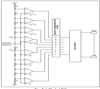
Conceptually, in the flash architecture (Fig. 2), a set of 2n-1 comparators is used to directly measure an analog signal to a resolution of n bits. For a 4-bit flash ADC, the analog input is fed into 15 comparators, each of which is biased to compare the input to a discrete transition value. These values are spaced one least-significant bit (LSB=FS/2n) apart. The comparator outputs simultaneously present 2n-1 discrete digital output states.
For an N-bit converter, the circuit has 2N-1 comparators. A resistive divider network with 2N resistors provides the reference voltage. Each comparator produces a 1 when its analog input voltage is higher than the reference voltage applied to it. Otherwise, the comparator output is "0". A regenerative latch at each comparator output stores the result.
Fig. 2 A Flash ADC
3.1.1 Sources of error
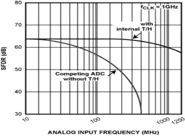
When the input signal changes before all the comparators have completed their decision, the ADC performance is adversely impacted. The most serious impact is a drop-off in signal-to-noise ratio plus distortion (SINAD) as the frequency of the analog input frequency increases. This can be removed by adding a track-and-hold (T/H) circuit in front of the ADC. This effect has been discussed in [5]. It allows dramatic improvement, especially when input frequencies approach the Nyquist frequency, as shown in Fig. 3
Fig. 3 SFDR as a function of input Frequency
Sparkle Codes
Normally, the comparator outputs form a thermometer code, such as 00011111. Errors may cause an output like 00010111. The spurious "0" in the result sequence is called a sparkle. This can be due to imperfect input settling or comparator timing mismatch. The magnitude of the error can be quite large and can be avoided by employing an input track-and-hold in front of the ADC along with an encoding technique that suppresses sparkle codes [14].
Metastability
When a digital output of a comparator is ambiguous i.e. neither a one nor a zero, the output is defined as metastable. Metastability can be reduced by allowing more time for regeneration. Gray-code encoding can be used to improve metastability. Gray-code encoding allows only one bit in the output to change at a time. The comparator outputs are first converted to gray-code encoding and then later decoded to binary. Another problem occurs when a metastable output drives two distinct circuits. It is possible for one circuit to declare the input a "1" while assumes it's a "0". This can create major errors. To avoid this, only one circuit should sense a potentially metastable output.
Clock Jitter
Signal-to-noise ratio (SNR) is degraded when there is jitter in the sampling clock. This becomes noticeable for high analog input frequencies. To achieve accurate results, it is critical to provide the ADC with a low-jitter, sampling clock source [13].
3.1.2 Design Considerations and Implications
The flash architecture has the advantage of being very fast, because the conversion occurs in a single ADC cycle. The disadvantage of this approach is that it requires a large number of comparators that are carefully matched and properly biased to ensure that the results are linear. Since the number of comparators needed for an n-bit resolution ADC is equal to 2n-1, limits of physical integration and input loading keep the maximum resolution fairly low. 3.2 Pipelined ADC
desired resolution. In principle, a pipelined converter with p pipelined stages, each with an m-bit flash converter, can produce a high-speed ADC with a resolution of n = p*m bits using p*(2m-1) comparators.
Fig. 4 A Single Pipelined Converter Stage
Target applications for pipeline ADCs include communication systems, in which total harmonic distortion (THD), spurious-free dynamic range (SFDR), and other frequency-domain specifications are significant; CCD-based imaging systems, in which favorable time-domain specifications for noise, bandwidth, and fast transient response guarantee quick settling; and data-acquisition systems, in which time and frequency domain characteristics are both important. Fast and accurate N-bit conversions can be accomplished using at least two or more steps of pipelining. 3.2.1. Sources of error
Overlapping
The following condition should be met to correct for overlapping errors: L × M+K > N
where L is the number of stages, M is the coarse resolution of subsequent stages in the ADC circuit, K is the fine resolution of the final ADC stage, and N is the pipeline ADC's overall resolution. [15] [17] have put forth methods to implement this technique.
Most pipeline ADCs include digital error-correction circuitry that operates between the stages. Some pipeline quantizers have a calibration unit that compensates for unwanted side effects such as temperature drift or capacitor mismatch in the multiplying DAC.
Other difficulties:
Complex reference circuitry and biasing schemes.
Pipeline latency, caused by the number of stages through which the input signal must pass. Critical latch timing, needed for synchronization of all outputs.
Sensitivity to process imperfections that cause nonlinearities in gain, offset, and other parameters. Greater sensitivity to board layout, compared with other architectures.
3.2.2 Design Considerations and Implications
Pipelined converters achieve higher resolutions than flash converters containing a similar number of comparators. However this comes at the price of increasing the total conversion time from one cycle to p cycles. But since each stage samples and holds its input, p conversions can be carried out simultaneously. The total throughput can therefore be equal to the throughput of a flash converter, i.e. one conversion per cycle. The difference is that for the pipelined converter, latency equal to p cycles is introduced. Another limitation of the pipelined architecture is that the conversion process generally requires a clock with a fixed period. Converting rapidly varying non-periodic signals on a traditional pipelined converter can be difficult because the pipeline typically runs at a periodic rate. Some aspects to overcome these practical design considerations have been discussed in [3] [4] [15]-[17].
3.3. Successive Approximation ADC
SAR ADCs most commonly range in resolution from 8 to 16 bits and provide low power consumption as well as a small form factor [1] [2] [4]. This combination makes them ideal for a wide variety of applications, such as portable/battery powered instruments, pen digitizers, industrial controls, and data/signal acquisition.
Fig 5. Successive-approximations architecture
The SAR ADC implements a binary search algorithm. Therefore, while the internal circuitry may be running at several megahertz (MHz), the ADC sample rate is a fraction of that number due to the successive-approximation algorithm.
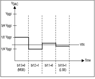
The analog input voltage (VIN) is held on a track/hold. To implement the binary search algorithm, the N-bit register is first set to midscale (that is, 100... .00, where the MSB is set to '1'). This forces the DAC output (VDAC) to be VREF/2, where VREF is the reference voltage provided to the ADC. A comparison is then performed to determine if VIN is less than or greater than VDAC. If VIN is greater than VDAC, the comparator output is a logic high or '1' and the MSB of the N-bit register remains at '1'. If VIN is less than VDAC, the comparator output is a logic low and the MSB of the register is cleared to logic '0'. The SAR control logic then moves to the next bit down, forces that bit high, and does another comparison. The sequence continues all the way down to the LSB. Once this is done, the conversion is complete, and the N-bit digital word is available in the register. Fig 6 illustrates an example of a 4-bit conversion
Fig 6. SAR operation (4-bit ADC example)
3.3.1 Sources of error
A SAR ADC's speed is limited by:
The settling time of the DAC, which must settle to within the resolution of the overall converter, for example, ½ LSB.
The comparator, which must resolve small differences in VIN and VDAC within the specified time.
The logic overhead.
A SAR converter can use a single comparator to realize a high resolution ADC. But it requires n comparison cycles to achieve n-bit resolution, compared to p cycles for a pipelined converter and 1 cycle for a flash converter. Since a successive-approximations converter uses a fairly simple architecture employing a single SAR, comparator, and DAC, and the conversion is not complete until all weights have been tested, only one conversion is processed during n comparison cycles. For this reason, SAR converters are more often used at lower speeds in higher-resolution applications. SAR converters are also well suited for applications that have non-periodic inputs, since conversions can be started at will. This feature makes the SAR architecture ideal for converting a series of time-independent signals [2]. [22]- [23] suggest methods for high-speed low-power structures for SAR ADCs.
Another consideration when using a SAR ADC is aliasing. The process of sampling a signal leads to aliasing - the frequency-domain reflection of signals about the sampling frequency. In most applications, aliasing is an unwanted effect that requires a low-pass anti-alias filter ahead of the ADC to remove high-frequency noise components, which would be aliased into the passband. However, undersampling can put aliasing to good use, most often in communications applications, to convert a high-frequency signal to a lower frequency. Undersampling is effective as long as the total bandwidth of a signal meets the Nyquist criterion (less than one-half the sampling rate), and the converter has sufficient acquisition and signal sampling performance at the higher frequencies where the signal resides. Considerable research is being expended into the SAR architecture based upon these design considerations.
3.4. Sigma-Delta ADC
The sigma-delta architecture takes a fundamentally different approach from the rest of the architectures. Sigma-delta converters offer high resolution, high integration, and low cost, making them a good ADC choice for applications such as process control and weighing scales. Considerably less work has been done on Sigma-delta ADCs as compared to other architectures.
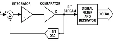
In its most basic form, a sigma-delta converter consists of an integrator, a comparator, and a single-bit DAC, as shown in Fig 7. The output of the DAC is subtracted from the input signal. The resulting signal is then integrated, and the integrator output voltage is converted to a single-bit digital output by the comparator. The resulting bit becomes the input to the DAC, and the DAC's output is subtracted from the ADC input signal, etc. This closed-loop process is carried out at a very high "oversampled" rate. The digital data coming from the ADC is a-stream of ones and zeros, and the value of the signal is proportional to the density of digital ones coming from the comparator. This bit stream data is then digitally filtered and decimated to result in a binary-format output [1]-[5].
Fig 7. Sigma-delta ADC architecture
3.4.1 Sources of Error
3.4.2 Design Considerations and Implications: Oversampling
In the frequency-domain transfer function of a traditional multi-bit ADC with a sine-wave input signal, the input is sampled at a frequency Fs. According to Nyquist criterion, Fs must be at least twice the bandwidth of the input signal. When observing the result of an FFT analysis on the digital output, a single tone and lots of random noise extending from DC to Fs/2 are observed (Fig 8). This effect is known as quantization noise and results from the following consideration: the ADC input is a continuous signal with an infinite number of possible states, but the digital output is a discrete function whose number of different states is determined by the converter's resolution. So, the conversion from analog to digital loses some information and introduces some distortion into the signal. The magnitude of this error is random, with values up to ±LSB [24].
Fig. 8 FFT diagram of a multi-bit ADC with a sampling frequency Fs
When the sampling frequency increased by the oversampling ratio k, to kFs (Fig. 9) the SNR remains unchanged but the noise energy is spread over a wider frequency range. Sigma-delta converters exploit this effect by following the 1-bit ADC with a digital filter. The RMS noise is less, because most of the noise passes through the digital filter. This action enables sigma-delta converters to achieve wide dynamic range from a low-resolution ADC.
Fig. 9 FFT diagram of an oversampled multi-bit ADC
Noise Shaping
One of the most advantageous features of the sigma-delta architecture is the capability of noise shaping, a phenomenon by which much of the low-frequency noise is effectively pushed up to higher frequencies and out of the band of interest. As a result, the sigma-delta architecture has been very popular for designing low-bandwidth high resolution ADCs for precision measurement [24]-[25].
4. Application Examples
Example 1: Multiple inputs, 16-bit resolution
Consider an application that requires 16-bit resolution for 4 independent signals with bandwidths of dc to 15 kHz, 15 kHz, 15 kHz, and 45 kHz.
throughput and effective throughput for each converter and indicates the number of converters of its type that would be needed to serve in this application:
Table 1
Example 2: Single input, 16-bit resolution
To convert a single 90-kHz bandwidth input at 16-bit resolution, all three converters from the first example can work well. Here the choice among converters would be made on other considerations, including ac and dc performance, system-level considerations (e.g. is there a great benefit to the anti-alias performance of sigma-delta converters in this application), latency, and cost.
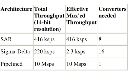
Example 3: Multiple inputs, 14-bit resolution
For an application in which 16 inputs, each with a dc to 100 kHz bandwidth, are converted with a resolution of at least 14 bits, three converters suitable for this application include the SAR-type, the sigma-delta, and the pipelined. The total throughput required under the Nyquist criterion is 2*100 kHz*16 = 3.2 MSPS. Table 2 shows the throughput for each converter.
Of the three converters, only the Pipelined has the throughput needed to convert all 16 channels. The SAR has sufficient throughput for 2 inputs per converter. To use the SAR in this application, 8 converters would be needed. The Sigma-Delta would need to be used in a converter-per-channel implementation; thus 16 converters would be required.
Table 2.
Architecture Total Throughput (16-bit resolution)
Effective Mux'ed Throughput
Converters needed
SAR 200 ksps 200 ksps 1
Sigma-Delta 195 ksps 2.3 ksps 4
Pipelined 2500 ksps 75 ksps 3
Architecture Total Throughput (14-bit resolution)
Effective Mux'ed Throughput
Converters needed
SAR 416 ksps 416 ksps 8
Conclusion
Various types of ADCs have been studied and their architectures have been analyzed. The design constraints and sources of errors for all architectures have been highlighted to draw a fair comparison of all architectures. The Applicability of these different types of ADCs for specific real time applications has also been outlined with the help of some specific examples.
References
[1] Analog-Digital Conversion Handbook (1986): The Engineering Staff of Analog Devices, Inc. Englewood Cliffs, NJ: Prentice Hall,. ISBN
0-13-032848-0.
[2] Practical Analog Design Techniques, (1995) edited by Walt Kester. Norwood, MA: Analog Devices, Inc. ISBN 0-916550-16-8.
[3] High Speed Design Techniques (1996) edited by Walt Kester. Norwood, MA. Analog Devices, Inc., 1996. ISBN 0-916550-17-6.
[4] Bruce, J.W., II.; Meeting the analog world challenge (Dec 1998-Jan 1999): Nyquist-rate analog-to-digital converter architectures,
Potentials, IEEE, Volume 17, Issue 5 pp. 36 – 39.
[5] Soenen E. (2001): Technology Tradeoffs in the Design of High Performance Analog to Digital Converters, IEEE Explore, pp. 7-11.
[6] Kim, S., Song, M. (2001): An 8-bit 200MSPS CMOS A/D converter for analog interface module of TFT-LCD driver. In: IEEE international
symposium on circuits and systems pp. 528– 531.
[7] Srinivas, V., Pavan, S., Lachhwani, A., Sasidhar, N. (2006): A distortion compensating flash analog-to-digital conversion technique, IEEE
Journal of Solid-State Circuits, 41(9), pp. 1959–1969. doi:10.1109/JSSC.2006.880601.
[8] Scholtens, P. C. S., Smola, D., Vertragt, M. (2005): Systematic power reduction and performance analysis of mismatch limited ADC
designs, International symposium on low power electronics and design pp. 78–83.
[9] Yoo, J., Lee, D., Choi, K., Kim, J. (2002): A power and resolution adaptive flash analog-to-digital converter, International symposium on
low power electronics and design pp. 233– 236.
[10] Tangel, A., Choi, K. (2004): The CMOS inverter as a comparator in ADC designs. Analog Integrated Circuits and Signal Processing, 39(2),
pp. 147–155. doi:10.1023/B:ALOG.00000 24062.35941.23.
[11] Sundström, T., Alvandpou, A. (2009): A 6-bit 2.5-GS/s flash ADC using comparator redundancy for low power in 90 nm CMOS, Journal of
Analog Integrated Circuits and Signal Processing, pp 0925-1030 (Print) 1573-1979 (Online).
[12] Hwang, Y., Huang, P., Hwang, B., Chen, J. (2009): An efficient power reduction technique for CMOS flash analog-to-digital converters.
Analog Integrated Circuit Signal Processing 61:pp. 271–278 DOI 10.1007/s10470-009-9309-7.
[13] Zhang, C., Shao, Z., (2009): Analysis and simulation of distributed T/H with averaging technique in folding and interpolating A/D
converters, Int. J. Circ. Theory. Appl. Published online in Wiley InterScience, DOI: 10.1002/cta.603.
[14] Gumenyuk, A. S., Bocharov, Y. I., (2008): Power-Reduction Techniques for CMOS Pipelined ADCs, Russian Microelectronics, Vol. 37,
No. 4, pp. 253–263.
[15] Ross, S.W., Sinha, S. (2007): A Pipeline Analogue to Digital Converter in 0.35 μm CMOS, EUROCON 2007 The International Conference
on “Computer as a Tool”, Warsaw, September 9-12.
[16] Lu, C., Lee, T., (2007): A 10-bit 60-MS/s Low-Power CMOS Pipelined Analog-to-Digital Converter, IEEE Transactions On Circuits And
Systems—II: Express Briefs, VOL. 54, NO. 8.
[17] Hwang, Y., Chen, J., Wu, S., Liao, L., Tsai C (2007): A new pipelined analog-to-digital converter using current conveyors, Analog Integr
Circ Sig Process 50:213–220 DOI 10.1007/s10470-007-9031-2.
[18] Rarbi, F., Dzahini, F. (2008) :A low power 12-bit and 30-MS/s pipeline analog to digital converter in 0.35μm CMOS, IEEExplore.
[19] Behnam, S., Sharif, B.M. (2009): Linearity analysis in pipeline A/D converters, Int. J. Circ. Theory, 37, pp.764–780.
[20] Mingjun, F., Junyan, R., Ning, L., Fan, Y., Jun, X. (2010): A 1.8-V 11-bit 40-MS/s 21-mW pipelined ADC, Analog Integr Circ Sig Process
DOI 10.1007/s10470-010-9453-0.
[21] Siva, R. K., Baghini, S. M., Mukherjee, J. (2009): Current-Mode CMOS Pipelined ADC, IEEExplore.
[22] Khosrov, D., Hadidi, K., Khoei, A. (2004): A New Architecture for Area and Power Efficient, High Conversion Rate Successive
Approximation ADCs, IEEExplore, pp 253-256.
[23] Khosrov, D., Hadidi, K., Khoei, A. (2006): A new successive approximation architecture for high-speed low-power ADCs, Int. J. Electron.
Commun. (AEÜ) 60, pp. 217 – 223.
[24] Sangil, P. (1993): Principles of sigma-delta modulation for Analog to digital converters, The communications Application Manual, Vol.
DL411D/REV1, Motorola Inc., Phoenix, pp. 293-350.
[25] Strak, A., Gothenberg, A., Tenhunen, H. (2004): Analysis of Clock Jitter Effects in Wideband Sigma-Delta Modulators for