222
Design And Development Of S-Band Power
Amplifier Module For Satcom Manpack Terminal
Pratiksha R Matlawar, Shambulinga M, Poornima P
Abstract: Communication via satellite is one of the prominent and widely used method for transmission of data. It is significant as it provides reliable and uninterrupted communication. Satcom Manpack terminal is light weight and portable equipment used in military applications. The operating frequency and output power delivered is the vital point of concern. Communication in remote areas has to be taken into consideration for better transmission between the end users. The module used in the project is selected from Qorvo with part number TGA2830 which provides higher output power, higher gain and low phase noise. This work focuses on the design and development of S-Band Power Amplifier (PA) module for Satcom Manpack terminal. The PA module is simulated, developed and tested for various performance parameters like output power, phase noise and spurious. It was observed that the results were matching the desired specifications.
Index Terms: GaN, Manpack Terminal, Output power, Phase noise, Satcom, S-band, Spurious.
—————————— ——————————
1.
INTRODUCTION
Satellite communication (Satcom) has got a wide range of applications which helps in transmitting and receiving of data via satellite. This kind of infrastructure have been used all around the world including remote and rural areas [1]. Satcom have been used in various applications like military, maritime railways and many more [2]. This development has become widespread in the fields like weather reporting, disaster relief operations and military which was difficult to be carried out in the isolated areas [3], [4]. One such innovation is a Satcom Manpack Terminal. As the name suggests it is a backpack carried by a man on his back, and enables convenient even in remote areas. For any manpack terminal the communication is through satellite which receives the information from the terminal present in the ground station and transmits back the signal to the assigned base station which further passes the signal to the respective terminal. A manpack family includes a modem, RF front end, antenna, interface display and power supply are common subsystems used to establish the communication via satellite. Gallium-nitride-based high-electron mobility transistors (GaN-HEMTs) are proved one of the best candidates for high-power and are used in much higher temperature microwave applications because of their better and attractive material properties which delivers high power 200W but limits the frequency at 430MHz [5], like large bandgap and electron saturation velocity higher than other materials, AlGaN/GaN buffer with large channel thickness effects the DC and RF performances [6]. The depletion mode devices require special bias sequencing to avoid the damage to the device. GaN being one such device requires a positive drain voltage and negative gate voltage to handle the drain current.
Onboard gate pulsing and bias sequencing provides one platform to work with GaN transistors operating at lesser frequency range [7]. In order to overcome the difficulties faced in the military application a portable equipment is developed with better performance. Manpack is suitable for transmission of data at remote location, with the transmitter (Tx) path having GaN based PA module which allows higher output power with less dissipation due to its broad band gap operating at S-Band range [8] In this paper the design and development of PA module operating in S-Band for Manpack terminal used in military application. The PA module TGA2830 from Qorvo operates in S-Band. The modules have been selected based on the required specifications, to study and understand the performance of the opted modules Advance Design System (ADS) CAD tool is used to note the output power levels at each module end. The integrated PA module is tested under laboratory conditions. Section 2 gives the description on the Satcom Manpack terminal, Section 3 provides the design and simulation of the PA module using ADS, Section 4 focuses on the outcomes and its analysis and Section 5 enlightens on the conclusions drawn from the project and future scope and limitations.
2
SATCOM
MANPACK
TERMINAL
A Manpack is a transceiver system which is used either in military or in commercial applications. The Manpack is a portable, light weight and easy to operate system and allows the transmission of data and voice. For any Manpack terminal the communication is via satellite which receives the information from the terminal present in the ground station and transmits back the signal to the assigned base station which further passes the signal to the respective terminal. Any Manpack family includes a digital section, RF front end, antenna, interface display and power supply which are common subsystems used to establish the communication via satellite.
2.1 Subsystems of Manpack Terminal
The module consists of a L-band modem as specified which is the digital section and the output of the modem is fed to the Tx path via diplexer and enters Receiver (Rx) path operating at S-band. fig. 1 shows the Manpack terminal module for S-band with diplexer and Tx-Rx antenna. The Tx path consists of up- converter, PA connected to the diplexer, similarly the Rx consists of LNA and down converter. Mixer is a 3-port device ————————————————
Pratiksha R Matlawar is currently pursuing master’s degree program in Radio Frequency and Microwave engineering in RV College of Engineering, India, PH-8861572331. E-mail: [email protected] Shambulinga M, Assistant Professor, Dept. of Telecommunication, RV
College of Engineering, India, PH-9916292488. E-mail:
Poornima P, Deputy engineer, Dept. of SATCOM, Alpha Design
Technologies, Pvt Ltd., India, PH-8310326610. E-mail:
223 with nomenclature of each port as RF, LO and Intermediate
Frequency (IF). The LO is either sinusoidal or square wave, depending on the application the wave is chosen, for a mixer LO is considered as gateway when the voltage is high it is ON and OFF when the voltage is low. LO is the input port and the other two ports can be interchanged as per the requirements represented as shown in (1). When the output is greater than the second input this process is called up-conversion. Similarly, the Rx section a down converter is used to convert the signal and feed it to the modem [9]. The concept of LO, RF and IF remains the same in up-converter, when the required output is lesser than the second input that method is called as down-conversion where RF and IF are input and output respectively shown (2).
(1) (2)
The next component in the system is GaN PA which requires a bias sequence to operate as the device is in depletion mode which means the device is always in the ON condition. In order to protect the device from damaging it requires a bias sequence, PA requires negative gate voltage and positive drain voltage. To make sure that the device does not affect any other components in the circuit the bias has to be followed for GaN PA [7], the negative gate voltage is applied first and then positive drain voltage is applied if this sequence is not followed before applying RF signal the transistor will draw more drain current through the supply which increases the thermal dissipation and damages the device. A diplexer is a 3-port device which separates the signal from the common port to the other 2 ports depending on the frequency. Diplexer can be used to show paths to two dissimilar receivers grounded on frequency, it can also be used as a bias tee to feed an active device through DC power. Diplexers designs provide high isolation which is appropriate for many applications, it allows a common channel for communication and makes the usage economical and low cost.
Fig 1: General block diagram satcom manpack terminal
Satellite communication has encouraged the wireless communication applications which uses an antenna as an important component which helps in proper communication between the Tx and Rx. Antennas are used by radio Tx or Rx for the coupling of electrical linking to the EM field. Antennas are basically directional which radiate in a single direction or omnidirectional which means radiating equally in all direction which is not practically possible. In any receiver a key component that is used is LNA to amplify the incoming signal from the antenna to reduce the noise, and a down converter stage. LNA is used in the received path enhances the signal strength and reduces the noise in satellite communication. As
the name suggests it adds very less noise to the received signal, the accepted signal is converted to information and it is placed near to the Rx to reduce the noise owed to interference. When the signal-to-noise ratio (SNR) is higher and requests to be tainted by about 50 out of a hundred and power desires to be enhanced, an LNA is used. How much amount of noise is added by the receiver to the signal is an important measurement which is called Signal to Noise Ratio (S/N), noise factor is the measure of how this S/N is tarnished and is given as F (noise factor) (3)
(3)
3
DESIGN
AND
SIMULATION
The design of S-band PA is carried out using ADS tool with the help of specifications provided in the datasheets of each component selected and simulated to analyse the performance of the PA. The design specifications are described in the coming sections and the block diagram representation used in the project is also shown to understand the flow of achieving the required parameters.
3.1 Design and Simulation of S-band PA
The specifications required to design the S-band PA module for Satcom Manpack terminal are shown in the Table 1. The specifications given in the below table are chosen based on the requirement for the application and each of the parameter has its own worth. Fig. 2 shows the block diagram of the S-band PA chain used in Satcom manpack terminal. Each component with their respective gain or loss is mentioned in the figure and the power levels at each component is shown based on component gain or loss. The Single Pole Double Throw (SPDT) switch is the first component in the PA chain with insertion loss (IL) of 2dB, the input to SPDT is the output from the modem. Switch has a single input and can link to and switch between two outputs. This means it has one input terminal and two output terminals. It can assist as an on-off switch, reliant on how the circuit is wired. SPDT switch before Power Amplifier is mainly used to cut off or on the RF path gain to PA.
Fig. 2: Block Diagram of S-band PA
TABLE 1
Design Specifications of PA module
Sl. No. Parameters Specifications
01 Transmit Bandwidth 20 MHz
02 Gain 31-28dB
03 PA Output Power +34 to +40 dBm
04 Phase noise @ 1 kHz offset < -55 dBc/Hz
05 Drain Voltage 28V/ 1A
06 Gate Voltage -5V/-2.7V
-224 50dBc/Hz
The second component in the chain is the driver amplifier (DA), which is used to drive the Power Amplifier. It requires minimum level to amplify, Modem may not generate enough power level to drive PA hence a DA stage is used to give enough power level for the amplifier to amplify. The operating voltage of DA is 5V which is supplied externally and it provides gain of 10dB. Table 2 shows the S-parameters considered for designing of DA. The next component is the BPF which basically filters out unwanted signal and passes only the intended frequency signal with insertion loss of 2dB. The next stage in the chain is the key component of the whole design, the PA module which is a GaN based device TGA2830 from Qorvo is suitable for the required specification. As discussed earlier the GaN requires a bias sequence in order to use the device without any damage. The module uses two power supply voltages one is to provide a negative gate voltage of -5V/-2.7V and other is for a positive drain voltage of 28V, the output of the PA is expected to be 40dBm (10W). The S-parameters of PA is given in Table 3. The PA output is fed to the next component in the chain that is a circulator module which has a very negligible loss of 0.25. As seen in the figure the circulator is a 3-port device which receives input from the PA, output to the directional coupler and the other port is grounded with 50Ω resistance. The circulator is placed after the PA module to make sure that there is no reverse flow of signal to the PA which may cause damage to the device, the circulator assures that the signal flow is always in one direction.
TABLE 2 S-Parameters of DA
S11 S12 S21 S22
-11.393/ 176.053
-18.915/ -13.593
12.670/6 0.538
-15.356/ -176.164
TABLE 3 S-Parameters of PA
S11 S12 S21 S22
-20.443/ -143.003
-59.101/ 82.53
31.269/-132.66
-12.013/ -73.619
Fig. 3: ADS Schematic of PA Module
The final stage used in the PA chain is a directional coupler (DC), which is designed as per the requirement. The DC has a main line (ML) and a coupled line (CL), the EM power in the transmission line is coupled to the enabled port connecting the other circuit. The DC coupling factor is used to provide a better power at the output. The detector placed in the CL is to monitor the voltage and current levels in the PA chain, suppose there is large voltage or current drawn in the circuit it
detects and disables the chain from getting damaged. The microstrip coupled line is designed at center frequency of 2.68GHz for proper coupling and isolation the width (W), spacing (S) and length (L) are optimized as W=1.4mm, S=0.5mm and L=10mm. The dielectric constant (ɛr) is 3.66. The ADS design involves the components in the S-band PA chain module, the chain includes SPDT switch, DA, BPF, Attenuator, PA module, circulator and a directional coupler. Each component is connected in the sequence as shown in Fig. 3 and the power levels at each component is shown and verified with the specifications. The Harmonic simulation is used to give the power levels and S-parameter simulation is for the input output return losses computation.
4
RESULTS
AND
DISCUSSIONS
The simulated design using ADS outcomes are discussed and analyzed in this section. In the later part of the section the implementation of the hardware tested in the laboratory are discussed.
4.1 Simulated Outcomes
The input to the SPDT switch is given from the supply, as the first component present in the PA module is the SPDT switch. The outcome of the SPDT switch shown in Fig. 4 includes the loss of the switch which is 2dB, so the input to the switch undergoes a loss of 2dB at its output. The gain included in the input power the outcome is 8.7dB, x and y axis represent frequency and output power respectively.
Fig. 4: Output of SPDT
Fig. 5: Output of DA
225 which is observed in the Fig. 5. It is also noted that the DA
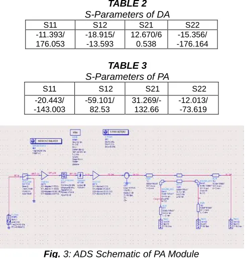
produces harmonics at even and odd multiplies of the fundamental frequency, the output is 19.8dBm can be observed from the figure. The harmonics present in the DA are reduced by using BPF, the outcome is observed to be 17.6dBm which includes the BPF loss of 2dB which means that the power is degraded by 2dB as shown in Fig. 6. It can be observed that the harmonics is reduced when it is compared with the DA outcome.
Fig. 6: Output of BPF
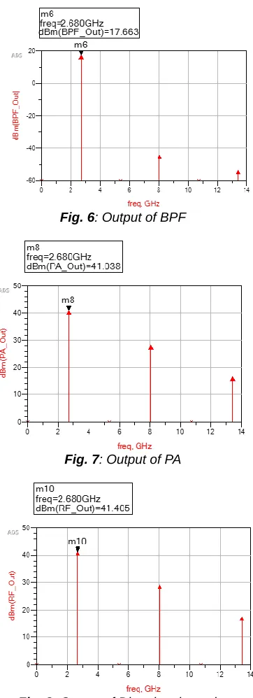
Fig. 7: Output of PA
Fig. 8: Output of Directional coupler
The PA module receives the incoming signal from the attenuator. The signal which as to be given to the diplexer the PA signal has to be improved and the power level should be increased by certain amount. The PA module has a gain of 27dB at the fundamental frequency, the output power level of
the PA is shown in Fig. 7. Coupler has a loss of 0.5dB which does affect the PA output, the coupled port is connected to the detector for voltage detection. The simulated results display that the power level of directional coupler is 41.40dBm as seen in Fig. 8
4.2 Hardware Implementation and Outcomes
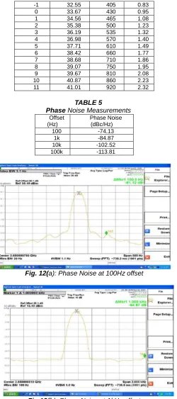
As discussed before the PA module schematic is designed using ADS and the module is fabricated and test results are discussed in the below section. The fabricated module using the specified PCB details are tested in the laboratory, Fig. 9 gives the layout of the PA module generated using PCB Planner software tool. the test setup is shown in Fig. 10For various input power levels, the output power levels of PA are noted down by subtracting the output from the input the gain is observed. Table 4, shows the power output levels of PA module which varies linearly with input power and Fig. 11 shows the output power at 10dBm input displayed on the spectrum analyzer. Phase noise is better than -50dBc/Hz for 100Hz, 1KHz, 10KHz and 100KHz offset. The detector placed in the CL is to monitor the voltage and current levels in the PA chain, suppose there is large voltage or current drawn in the circuit it detects and disables the PA chain from getting damaged. The corresponding Vrms measured at the various input power levels are shown in the Table 4.
Fig. 9: Layout of the PA module
Fig. 10: Test Setup of PA module
TABLE 4
Power output levels and corresponding Voltages Pin
(dBm)
Pout
(dBm) Id (mA)
Vrms( V)
-5 28.26 260 0.52
-4 29.12 330 0.61
-3 30.93 355 0.69
226
-1 32.55 405 0.83
0 33.67 430 0.95
1 34.56 465 1.08
2 35.38 500 1.23
3 36.19 535 1.32
4 36.98 570 1.40
5 37.71 610 1.49
6 38.42 660 1.77
7 38.68 710 1.86
8 39.07 750 1.95
9 39.67 810 2.08
10 40.87 860 2.23
11 41.01 920 2.32
TABLE 5
Phase Noise Measurements Offset
(Hz)
Phase Noise (dBc/Hz)
100 -74.13
1k -84.87
10k -102.52
100k -113.81
Fig. 12(a): Phase Noise at 100Hz offset
Fig.12(b): Phase Noise at 1kHz offset
The Table 5 gives the phase noise measured for different offsets at the center frequency and input power of 10dBm. Phase noise is the measure of noise produced by the PA with respect to the frequency at various offsets is shown in Fig. 12(a), (b), (c) and (d). Fig. 13(a) and (b) shows the spurious measured for both In-Band and Out-Band, the spectrum analyzer span is set for 100kHz for in-band and 1MHz for out-band. The RBW is set for 100Hz and VBW at 1Hz, the PA provides spurious both inband and outband is better than -50dBc.
Fig. 12(c): Phase Noise at 100kHz offset
Fig. 12(d): Phase Noise at 10kHz offset
Fig. 13(a): Spurious In-Band
227
5
CONCLUSION
S-band PA module is capable to provide sufficient amount of power for transmission of data from the Manpack terminal to base station via satellite. The signal is transmitted through various modules in the chain and the output is read at PA output. For input power levels from -5dBm to 11dBm is designed and simulated using ADS software tool. The assembled PCB is integrated and connected to required equipment for various parameter measurements. The output power measuring at various input levels shows that the output power varies linearly with input power. At input power 10dBm it is observed that the output power is 40dBm. Phase Noise is observed to be better than -50dBc/Hz for 1KHz,10KHz and 100KHz offsets. Gain is observed to be 30.87dB. spurious measured both in-band and out band is achieved -78.47dB and -65.34dB respectively. The design of manpack terminal includes GaN based PA which is used to provide a high power, but the power radiating from the manpack might affect the human body. As the manpack is carried on the back of human at very different terrains and weather it is important to take care on the radiation affecting the human body. As observed in the complete block diagram of manpack terminal the L-band modem can be replaced by a S-band modem which reduces the components incorporated in the system such as up-down converters, this in turn reduces the weight of the complete system and makes it easier to be carried on the back without much difficulty.
REFERENCES
[1] M. R. Effendi, R. Ernanto and A. Munir, "4.2GHz compact collinear antenna for manpack satellite communication," in Proceedings of 2018 International Workshop on Antenna Technology (iWAT), Nanjing, pp. 1-4, 2018.H. Sledzik, R. Reber, B. Bunz, P. Schuh, M. Oppermann M. Muber, M. Seelmann-Eggebert and R. Quay, "GaN based power amplifiers for broadband applications from 2GHz to 6GHz," in Proceedings of the 5th European Microwave Integrated Circuits Conference, pp. 416- 419, 2010. [2] W. L. Morgan and G. D. Gordon, Communications
Satellite Handbook, 1st ed., John Wiley & Sons, Inc., 1989.
[3] S. Ohmori, H. Wakana, and S. Kawase, Mobile satellite communications, Artech House, 1998.
[4] Gabriele Formicone, Jeff Burger, James Custer, Gianni Bosi, Antonio Raffo and Giorgio Vannini, ―Solid-State RF Power Amplifiers for ISM CW Applications Based on 100 V GaN Technology‖, in Proceedings of 11th European Microwave Integrated Circuits Conference, 3–4 Oct 2016.
[5] Xinhua Wang, Sen Huang, Yingkui Zheng, Ke Wei, Xiaojuan Chen, Haoxiang Zhang, and Xinyu Liu, "Effect of GaN Channel Layer Thickness on DC and RF Performance of GaN HEMTs With Composite AlGaN/GaN Buffer," in IEEE Transactions on Electron Devices, vol. 61, no.5, pp. 1341-1346, May 2014. Apet Barsegyan, VinodhThangam and Daniel Koyama, ―Bias Sequencing and Gate Pulsing Circuit for GaN Amplifier‖, in Proceedings of 10th International Radar Symposium India, Dec. 2015
[6] Krishna Prasad S, Shambulinga M, ―Design of Class F Power Amplifier for 2.4ghz using Third Harmonics‖ in Proceedings of International Journal of Recent Technology and Engineering (IJRTE), Volume-8 Issue-3,
Sept. 2019