Department of Electronic Engineering, Technological University (Lashio), Myanmar
DOI: 10.29322/IJSRP.9.05.2019.p8990 http://dx.doi.org/10.29322/IJSRP.9.05.2019.p8990
Abstract- Amplifiers are classified as untuned (wide band) amplifiers and tuned (narrow band) amplifiers based upon their bandwidth. Untuned amplifiers will provide the constant gain over a limited band of frequencies i.e., from lower to upper cut-off frequency. Tuned amplifiers will amplify signals of only fixed frequency of which is equal to the resonant frequency of the tuned circuit LC. In this paper, firstly, a basic small-signal (untuned) amplifier is designed as a swamped amplifier which is commonly used in electronic devices to use as a preamplifier. And then, its bandwidth (BW) is calculated estimably by subtracting lower cut-off frequency from upper cut-off frequency. After that, this amplifier design is converted into small-signal single tuned amplifier with center frequency 1M Hz and bandwidth of 20 kHz, to use as a radio frequency amplifier for a standard broadcast receiver by replacing a parallel tuned LC network in the collector circuit. In this paper, bandwidth of these two amplifiers is analyzed by Bode Plotter which shows the voltage gain (dB) versus frequency using Multisim 12.0. Finally, the difference of bandwidth between them is illustrated by simulation graph. It is observed that each design of amplifier amplifies signals within its rated ranges of frequencies (bandwidth).
Index Terms- swamped amplifier, single tuned amplifier, bandwidth, cut-off frequency, resonant frequency.
I. INTRODUCTION
mall signal voltage amplifiers are popular to amplify the small signal ac and they are configured mostly as common emitter BJT amplifiers. A swamped amplifier is also a common emitter amplifier in which some of the emitter resistor is unbypassed to get negative feedback for the stability of voltage gain [1]. This amplifier amplifies a wide band of frequencies equally well and does not permit the selection of a particular desired frequency and so it is called untuned amplifier. But sometimes, it is needed to design an amplifier that should select a desired frequency or narrow band of frequency for amplification and it is called tuned amplifier. Mostly, a tuned amplifier is designed to amplify the specified center frequency and is also called resonant frequency of this tuned circuit [3].
However, all amplifiers will amplify nicely any signal in their bandwidth. Bandwidth is the range of frequencies at which the voltage gain of the amplifier falls to 70.7% of the maximum gain. A frequency at which the voltage gain is 70.7% of its midrange value, expressed in dB as ( ) = 20 log (0.707) = −3 dB, is called cutoff frequency [1].
To convert the untuned amplifier into tuned amplifier, it is merely needed that the simple resistive load in the collector is replaced by a parallel tuned LC circuit whose impendence strongly depends upon the frequency. This paper is organized as follows. Section I is introduction about the tuned and untuned amplifiers. Design elaboration of swamped amplifier and single tuned amplifier including calculation of bandwidth are illustrated in section II. In section III, simulation results are expressed and conclusion for this work is presented in section IV.
II. DESIGN PROCEDURE AND CALCULATIONS
In this work, a swamped amplifier is designed according to the design protocol [2]. Firstly, design requirements are specified as the following:
Device is 2N3904 (npn);
ℎ = 100 (worst-case);
| |= 20; = 5kΩ;
= 12 V;
Lower cutoff frequency, = 50 Hz.
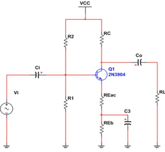
In design calculation, the value of resistors and capacitors are used for standard values and checking of voltage gain is also made. The circuit diagram of a swamped amplifier is shown in figure 1.
Figure 1: Schematic diagram of a swamped amplifier
A. Design Calculations for Swamped Amplifier
Let = = 5.1kΩ for maximum power transfer, [R= // = 2.5kΩ]
= ( ) | | . | |
( )( )| | = = 1.5 mA (1)
From data sheet, at = 1.5 mA, ℎ = 2.5kΩ, ℎ = 130.
= |. | | |= 104.19≈ 100Ω (2)
= ( ) = 233Ω ( = 4.35≈4 at = 1.5mA) (3)
= − = 233-100 = 133Ω ≈130Ω
For simplicity, using the 10% stability rule, = 10% (ℎ ) = 0.1 (ℎ ) = 2.3 kΩ (4)
= 1 + 1ℎ + + = 1.08V (5)
= = 2.5kΩ (6)
= = 26.28k ≈ 27kΩ (7)
=
. = - 20.66 (ok) (checking ) (8)
= ∥ ∥(ℎ + 1 +ℎ )= 1.91kΩ (9)
= = 5.1 kΩ (10)
= . = . . × = 2.5µ≈2.2µF (11)
= (. ) = .
× . = 0.48µ≈0.47µF (12)
are used for blocking dc and the values of these capacitance are used to set the -3dB low cutoff point at 50Hz. For , taking 10 ≤ , = 100µF.
[image:2.612.174.438.59.302.2]C = = 177pF (C= + + ) (16)
At = 1.5 mA, = 0.82 = 0.82 ( − − ) = 135pF ( is diffusion capacitance) (17)
C = 135PF + 12 = 147 PF (18)
= . ( ) = 296MHz (19)
The first high frequency corner, is, = | ×| = . × ≈ 30MHz (20) BW= - = 30MHz − 50Hz ≈ 29 MHz which is nearly . (21)
C. Design converting from swamped amplifier to single tuned amplifier
In this work, an RF amplifier having 20 kHz bandwidth at 1.0MHz center frequency is chosen to design as single tuned amplifier using the above amplifier.
Choosing L=10 µH, the required design calculations are as follows:
Resonant frequency, = 1 MHz;
=
√ and so C= 2.5nF (22)
For bandwidth, BW= 20 kHz;
Upper cutoff frequency, = + 10 kHz = 1.01 MHz (23) Lower cutoff frequency, = − 10kHz = 0.99 MHz (24)
III. SIMULATION RESULTS
Each designed amplifier is simulated using Multisim 12.0. Figure 2 shows the complete design of swamped amplifier with input signal 50mVpk at frequency 1kHz and figure 3 shows the graph of voltage gain versus frequency for this amplifier.
Figure: 3 Graph of voltage gain versus frequency of swamped amplifier
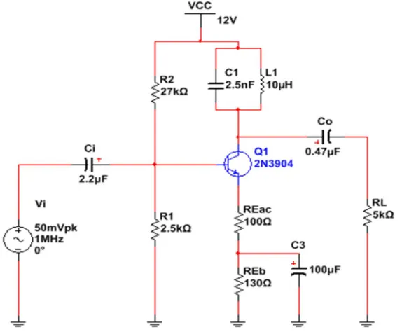
[image:4.612.166.453.253.490.2]Also, a complete design of single tuned amplifier with input signal 50mVpk at frequency 1MHz is shown in figure 4 and the graph of voltage gain versus frequency for this amplifier is shown in figure 5.
Figure 4: Complete design of single tuned amplifier
Figure 5: Graph of voltage gain versus frequency of single tuned amplifier
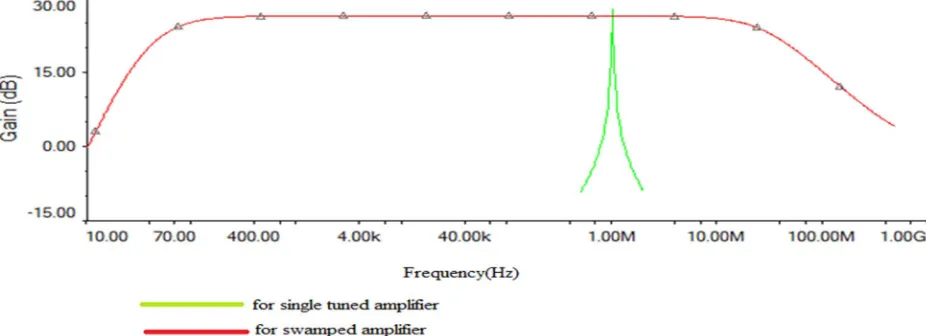
[image:4.612.71.550.559.662.2]Figure 6: Comparison of bandwidth between these two amplifiers
Now, analysis of the value of bandwidth for these two amplifiers is started. As the voltage gain (dB) of swamped amplifier is 26.42dB, the value of voltage gain (dB) of this amplifier which falls to 70.7% of the maximum gain is nearly 23dB. Figure 7 shows the Bode plotters which indicate the value of lower and upper cut-off frequencies for the swamped amplifier.
lower cut-off frequency=57.735Hz (midrange gain≈26.42dB) upper cut-off frequency=30.642MHz at 23.108dB (≈down 3dB) at 23.022dB (≈down 3dB)
Figure 7: Bode plotters indicating the value of lower and upper cut-off frequencies for the swamped amplifier
Similarity, for the single tuned amplifier, according to Bode result, midrange gain is approximately 30.921dB at center frequency at 1.003MHz. Figure 8 shows the Bode plotters which indicate the value of lower and upper cut-off frequencies for the single tuned amplifier.
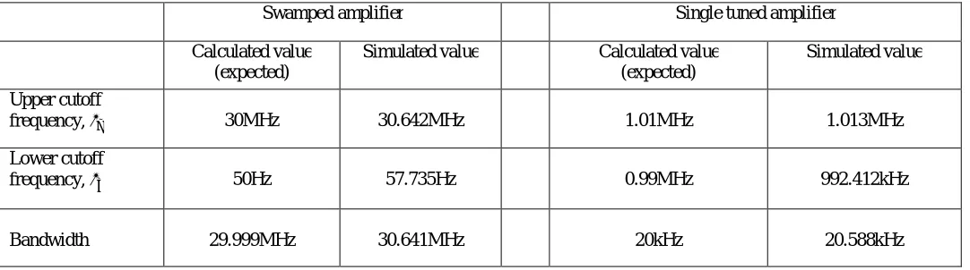
[image:5.612.35.596.301.472.2]According to the above figure 7 and 8, table 1 is made to study the comparison of calculated (expected) values and simulated values for swamped amplifier and single tuned amplifier approximately.
Table 1: Comparison of calculated (expected) values and simulated values for swamped amplifier and single tuned amplifier
Swamped amplifier Single tuned amplifier
Calculated value (expected)
Simulated value Calculated value (expected)
Simulated value
Upper cutoff
frequency, 30MHz 30.642MHz 1.01MHz 1.013MHz
Lower cutoff
frequency, 50Hz 57.735Hz 0.99MHz 992.412kHz
Bandwidth 29.999MHz 30.641MHz 20kHz 20.588kHz
IV. CONCLUSION
From the simulation results, the proposed design of swamped amplifier amplifies the input signals by the specified voltage gain in the wide ranges of frequencies. Its bandwidth is about 30MHz which is nearly equal to the upper cutoff frequency. Also, the single tuned amplifier amplifies only the signals at the specified center frequency, called resonant frequency 1MHz while discriminating all others. Moreover, according to the table 1, it can be observed that there is a little difference between calculated (expected) values and simulated values and so design evolution flow in this work is successful and convenient. But, for practical work, there is needed to concentrate about other facts such as temperature, power consume, the size of inductor, load and so on.
ACKNOWLEDGMENT
Firstly, the author would like to thank her beloved parents and her husband for their supports and encouragements to do this paper. The author also wishes to give her thanks to all teachers who teach her in her whole life.
REFERENCES [1] Thomas L. Floyd,"Electronic Devices"; Conventional Current Version,(Ninth Edition),2012.
[2] Glifford D.Ferris, "Elements of Electronic Design".Minneapoils/St.Paul.New York.Los Angeles.San Francisco,1995.. [3] Roy Blake, "Electronis Communication Systems",(Second Edition).
[4] https//www.tutorialspoint.com/amplifiers/types of tuned amplifiers.htm. [5] Steven T. Karris,"Electronic Device and Amplifier Circuits,(Third Edition).
AUTHOR
Thit Waso Khine – Lecturer, Department of Electronic Engineering, Technological University (Lashio), Myanmar.