International Journal of Emerging Technology and Advanced Engineering
Website: www.ijetae.com (ISSN 2250-2459,ISO 9001:2008 Certified Journal, Volume 3, Issue 12, December 2013)
70
A 10-bit 2MS/s SAR ADC Using a Dynamic Element Matching
Technique
Eun-Ju Choe
1, Seok Heo
2, Yong-Sik Kwak
3, Gil-Cho Ahn
4 1,3,4Dept. of Electronic Engineering Sogang University, Seoul, Korea
2Fairchild Semiconductor, Bucheon, Korea
Abstract—A 10-bit successive approximation register (SAR) analog-to-digital converter (ADC) using metal layer parasitic capacitance is presented. A data-weighted averaging (DWA) technique is adopted to attenuate the nonlinearity caused by the capacitor mismatch. A monotonic capacitor switching procedure is used to reduce the average switching energy and total capacitance. The proposed ADC fabricated in a 0.13μm CMOS process achieves a peak signal-to-noise and distortion ratio (SNDR) of 56.5 dB and a spurious free dynamic range (SFDR) of 65.1 dB with 2 MHz sampling frequency while consuming 3.12mW at a 1.2 V supply voltage.
Keywords—Analog-to-digital conversion, CMOS analog integrated circuit, data-weighted averaging, dynamic element matching, successive approximation register.
I. INTRODUCTION
Recent advances of system-on-a-chip (SoC) have led to the increasing demand for high performance analog-to-digital converters (ADCs) to simplify the system architecture and maximize the benefit of digital signal processing in the scaled down deep sub-micron CMOS technology. Among the various topologies of ADC, a successive approximation register (SAR) ADC is one of the most popular architectures for medium resolution, medium speed and low power applications due to its low analog circuit complexity and power efficiency [1].
A SAR ADC mainly consists of a comparator, a digital-to-analog converter (DAC) and SAR control logic. Among these, a DAC typically occupies the largest fraction of the area. So, it is strongly demanded to minimize the area of DACfor the reduction of the overall area.
In a conventional SAR ADC, a capacitive DAC is frequently used since it provides good device matching.
One of the most commonly used solutions to reduce the number of unit capacitors in a SAR ADC is a split capacitor structure [2, 3]. However, the bridge capacitor which has a fractional ratio value of a unit capacitance causes distortion due to its poor matching. Furthermore, the parasitic capacitances at both plates of the bridge capacitor also degrade a linearity performance. Another simple approach is to use a smaller size unit capacitor. However, limited capacitance matching of the small unit capacitor increases the nonlinearity of the ADC.
In this paper, we present a 10-bit SAR ADC that uses metal layer parasitic capacitance for a DAC. A data-weighted averaging (DWA) technique is employed to attenuate the harmonic distortion caused by the mismatch of small unit capacitor [4, 5]. To achieve further reduction of the area, a monotonic switching procedure is applied for the proposed SAR ADC. The paper is organized as follows. Section II discusses the architecture of the proposed SAR ADC. The details of the circuit implementation are described in Section III. The experimental results are shown in Section IV. Finally, Section V summarizes the conclusions drawn from the project.
II. PROPOSED SARADCARCHITECTURE
International Journal of Emerging Technology and Advanced Engineering
Website: www.ijetae.com (ISSN 2250-2459,ISO 9001:2008 Certified Journal, Volume 3, Issue 12, December 2013)
[image:2.612.75.535.124.538.2]71
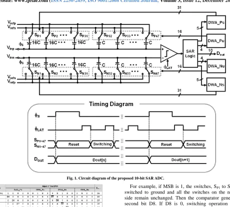
Fig. 1.Circuit diagram of the proposed 10-bit SAR ADC.
Fig. 2. Input bit sequence of the DWA logic.
Fig. 2 shows the input bit sequence of the DWA logic for each step. Operation of the proposed ADC is as follows.
S, input signal is sampled into the
capacitor array through the switches which are directly connected to the input of the comparator. After finishing the input sampling, the first comparison is performed and MSB is decided. According to the MSB output, SAR logic generates input bits of DWA_Ps and DWA_Ns as [6].
For example, if MSB is 1, the switches, SP1 to SP16, are
switched to ground and all the switches on the negative side remain unchanged. Then the comparator generates a second bit D8. If D8 is 0, switching operation on the negative side begins from SN1 and all the switches on the
International Journal of Emerging Technology and Advanced Engineering
Website: www.ijetae.com (ISSN 2250-2459,ISO 9001:2008 Certified Journal, Volume 3, Issue 12, December 2013)
72 Fig. 3 shows the switching procedures for 16 unit capacitors on the positive side of the ADC without and with the DWA control. Fig. 3(a) shows the conventional binary switching sequence which always selects same capacitor for the same digital input. So the nonlinearity resulted from capacitor mismatch in each step is always same and causes harmonic distortion. Fig. 3(b) shows the switching procedure with the DWA control. Unlike the conventional one, switching operation begins from the next unused available switch. So the capacitors used at each step are changed for each sampling period, and errors caused by the capacitor mismatch are randomized which improves a linearity of SAR ADC.
(a)
[image:3.612.332.552.252.641.2](b)
Fig. 3. Switching procedures for 16 unit capacitors on the positive side of the ADC (a) without DWA and (b) with DWA.
III. CIRCUIT IMPLEMENTATION
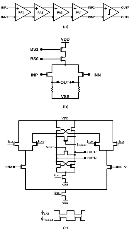
Fig. 4(a) shows the block diagram of the comparator which consists of four preamplifiers followed by a latch. Four stages amplifier is employed to reduce the meta-stability problem and kickback noise. Furthermore, the bandwidth of the overall stage is optimized by scaling the bias current and size of the input differential pair of each stage. Fully-differential common-source amplifier topology with a resistive load is used. In the first and the second stages (PA1, PA2), PMOS input differential pairs are employed as shown in Fig. 4(b). However, in the third and the fourth stages (PA3, PA4), NMOS input differential pairs are used to adjust the output common-mode level to the input common-mode of the following latch. The detailed circuit implementation of the latch is illustrated in Fig. 4(c). During the reset phase (RESET = VDD), OUPT
and OUTN are shorted together. When the both RESET and
LAT are low, the latch operates as an amplifier and tracksthe output signal of the preamplifier.
When the LAT is changed to high, the latch regenerates
the digital output signal.
Fig. 5 shows a layout floor plan of the half-cell of the DAC capacitor array. Each capacitor is connected to the switch with same number in Fig. 1. The cells denoted by D are dummy capacitors. Capacitor arrays are placed symmetrically to improve the matching. Instead of using the conventional MIM capacitor, metal line parasitic capacitance is used to minimize the area. The capacitance of the unit capacitor extracted from the layout is about 4fF.
+ + + + + OUTP
OUTN
PA1 PA2 PA3 PA4
INP2
INN2 INP1
INN1
(a)
INP INN
VSS VDD
BS0 BS1
-OUT+
(b)
LAT
RESET
(c)
Fig. 4. Circuit implementation of the comparator (a) block diagram of the comparator, (b) schematic of the preamplifiers PA1, PA2 and (c)
[image:3.612.58.279.284.452.2]International Journal of Emerging Technology and Advanced Engineering
Website: www.ijetae.com (ISSN 2250-2459,ISO 9001:2008 Certified Journal, Volume 3, Issue 12, December 2013)
73 D D D D D D D D D D D D D D D D D D D D D D D D D D D D D D D D D D D D 1 1 1 1 1 1 1 1 1 1 1 1 1 1 1 1 3 3 3 3 3 3 3 3 3 3 3 3 3 3 3 3 4 4 4 4 4 4 4 4 4 4 4 4 4 4 4 4 2 2 2 2 2 2 2 2 2 2 2 2 2 2 2 2 6 6 6 6 6 6 6 6 6 6 6 6 6 6 6 6 8 8 8 8 8 8 8 8 8 8 8 8 8 8 8 8 12 12 12 12 12 12 12 12 12 12 12 12 12 12 12 12 10 10 10 10 10 10 10 10 10 10 10 10 10 10 10 10 9 9 9 9 9 9 9 9 9 9 9 9 9 9 9 9 11 11 11 11 11 11 11 11 11 11 11 11 11 11 11 11 5 5 5 5 5 5 5 5 5 5 5 5 5 5 5 5 7 7 7 7 7 7 7 7 7 7 7 7 7 7 7 7 13 13 13 13 13 13 13 13 13 13 13 13 13 13 13 13 15 15 15 15 15 15 15 15 15 15 15 15 15 15 15 15 16 16 16 16 16 16 16 16 16 16 16 16 16 16 16 16 14 14 14 14 14 14 14 14 14 14 14 14 14 14 14 14 20 20 20 20 20 20 20 20 20 20 20 20 20 20 20 20 18 18 18 18 18 18 18 18 18 18 18 18 18 18 18 18 24 24 24 24 24 24 24 24 24 24 24 24 24 24 24 24 22 22 22 22 22 22 22 22 22 22 22 22 22 22 22 22 21 21 21 21 21 21 21 21 21 21 21 21 21 21 21 21 23 23 23 23 23 23 23 23 23 23 23 23 23 23 23 23 17 17 17 17 17 17 17 17 17 17 17 17 17 17 17 17 19 19 19 19 19 19 19 19 19 19 19 19 19 19 19 19 25 25 25 25 25 25 25 25 25 25 25 25 25 25 25 25 27 27 27 27 27 27 27 27 27 27 27 27 27 27 27 27 26 26 26 26 26 26 26 26 26 26 26 26 26 26 26 26 28 28 28 28 28 28 28 28 28 28 28 28 28 28 28 28 29 29 29 29 29 29 29 29 29 29 29 29 29 29 29 29 30 30 30 30 30 30 30 30 30 30 30 30 30 30 30 30 31 31 31 31 31 31 31 31 31 31 31 31 31 31 31 31
D D D D D D D D D D D D D D D D D D D D D D D D D D D D D D D D D D D D D D D D D D D D D D D
D D D D D D D D D D D D D D D D D D D D D D D D D D D D D D D D D D D D D D D D D D D D D D D D D D D D D D D D D D D D D D D D D D D D D D D D D D D D D D D D D D D D D D D D D D D D D D D D D D D D D D D D D D D D D D D D D D D D D D D D D D D D D D D D D D D D D D D D D D D D D D D D D D D D D D D D D D D D D D D D D D D D D D D D D D D D D D D D D D D D D D D D D D D D D D D D D D D D D D D D D D D D D D D D D D D D D D D D D D D D D D D D D D D D D D D D D D D D D D D D D D D D D D D D D D D D D D D D D D D D D D D D D D D D D D D D D D D D D D D D D D D D D D D
32 34 36 38 40 42 44 46 47 45 43 41 39 37 35 33
[image:4.612.62.278.386.561.2]Fig. 5.Layout floor plan of the half-cell of DAC capacitor array.
Fig. 6. Chip die photograph.
IV. MEASURED RESULT
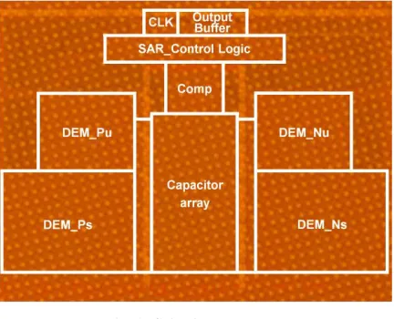
The prototype ADC is fabricated in a 0.13μm 1P 6M CMOS technology, and occupies 0.93mm2 active die area. The die photograph of the prototype chip is shown in Fig. 6. Fig. 7 shows the measured nonlinearity of the ADC without and with the DWA control. As shown in the measured results, nonlinearity errors at the segment transitions points are reduced by using the proposed technique.
The peak DNL and INL are -0.17/0.17 and -0.43/0.44 LSB, respectively. Fig. 8 shows the measured power spectrum of the output for a 200 kHz, -1 dBFS differential sinusoidal input signal. The prototype achieves a peak SNDR of 56.5 dB and a peak SFDR of 65.8 dB using a 2 MHz sampling frequency. Fig. 9 plots the measured SNDR and SFDR versus the input frequency at 2 MS/s. The power consumption with 1.2 V supply is 2.84 mW for the analog section, and 0.30 mW for the latch and the digital section. The performance is summarized in TABLE I.
V. CONCLUSION
International Journal of Emerging Technology and Advanced Engineering
Website: www.ijetae.com (ISSN 2250-2459,ISO 9001:2008 Certified Journal, Volume 3, Issue 12, December 2013)
74 (a)
[image:5.612.318.563.115.396.2](b)
Fig. 7. Measured DNL and INL (a) without DWA (b) with DWA
[image:5.612.64.279.134.491.2]Fig. 8. Measured output spectrum of the proposed SAR ADC.
Fig. 9. Measured SNDR and SFDR.
Table I. Performance summary
Technology 0.13 μm CMOS
Supply Voltage 1.2 V
Sampling rate 2 MHz
SNDR @ fin = 200kHz 56.5 dB
SFDR @ fin = 200kHz 65.1 dB
ENOB (bit) 9.1 bit
DNL -0.17/0.17LSB
INL -0.43/0.44 LSB
Power consumption Analog : 2.84mW
Digital : 0.295mW
Active area 0.93 mm2 (1.12mm x 0.83mm)
Acknowledgements
This work was supported by the IDEC of KAIST and the MSIP(Ministry of Science, ICT & Future Planning), Korea, under the University ITRC support program (NIPA-2013- H0301-13-1007) supervised by the NIPA. (Nation IT Industry Promotion Agency)
REFERENCES
[1] J. McCreary and P. Gray, ―All-MOS charge redistribution analog-to-digital conversion techniques,‖ IEEE J. Solid-State Circuits, vol. SC-10, no. 12, pp. 371–379, Dec. 1975.
[2] Yanfei Chen, Xiaolei Zhu, and Hirotaka Tamura, "Split Capacitor DAC Mismatch Calibration in Successive Approximation ADC," IEEE Custom Integrated Circuits Conference, pp. 279-282, 2009
[3] Ji-Yong Um, Yoon-Jee Kim, Eun-Woo Song, Jae-Yoon Sim,
Hong-June Park, ―A Digital-Domain Calibration of Split-Capacitor DAC for a Differential SAR ADC Without Additional Analog Circuits,‖ IEEE Trans. Circuits Syst. I, Reg. Papers, vol. 60, no. 11, pp. 2845– 2856, Nov. 2013.
[4] Marko Neitola and Timo Rahkonen, ―A Generalized Data-Weighted
Averaging Algorithm,‖ IEEE Trans. Circuits Syst. I, Reg. Papers, vol. 57, no. 2, pp. 115–119, Feb. 2010.
[5] Richard Schreier, and Gabor C. Temes, Understanding Delta-Sigma
Data Converters, Wiley Inc., New Jersey, 2005.
[image:5.612.64.260.510.662.2]