A High Speed Parallel Counter Architecture
and its Implementation in Programmable
Square Finder cum Frequency Divider Circuit
Pramod.P
Department of Electronics and Communication Engineering, Anna University Coimbatore Jothipuram, Coimbatore, Tamil Nadu, India
ABSTRACT
An 8-bit programmable square finder cum frequency divider architecture is presented. This special architecture includes a high speed parallel counter, clock trigger circuit, eight bit multiplier logic, sequence termination logic and sequence restarter logic. The entire architecture is divided into two parts: The frequency divider section and the square finder section. The frequency divider circuit outputs a sequence of states and the modulus is determined by the external frequency select input. The Square finder circuit finds the square of the given number by repetitively adding the number that much times. The counter consists of two main sections- the counting section and the state Anticipation Module. The 8-bit square finder cum frequency divider employing existing counter architecture [5] consumes a total transistor count of 1206 whereas the same using proposed counter architecture consumes only 1038. The worst case delay of the proposed programmable square finder cum frequency divider architecture employing the existing and proposed counter architecture was found to be 21.829ns and 20.686 respectively and the Power dissipation at 250 MHz was found to be 6.35 mW and 5.77mW respectively.
Keywords
Counter, Square, frequency divider, high speed, state anticipation module, sequence, modulus
1.
INTRODUCTION
Fast counter is a key element in most of the circuit operations such as frequency dividers, shifters and arithmetic operations such as multipliers. Basic properties preferred for a fast counter includes high count rate, read on the fly and implementation suitable for VLSI. Frequency dividers are basic blocks in numerous numbers of applications, such as generation of clock pulses of desired frequency, synchronization, data recovery and frequency synthesis in satellite communication systems. An innovative design of a square finder cum frequency divider architecture is carried out here. The entire architecture is divided into two parts: The frequency divider section and the square finder section.
As the speed of operation is determined by the propagation delay time of the count enable signal from the LSB to the MSB, most of the conventional frequency dividers and counters cannot satisfy the speed requirements. Therefore, the counter's size is considered to be the main limiting factor of the counting rate [I]. Some traditional approaches enhanced the counting speed by improving the circuit implementation of various gates and flip-flops, [2], [3], [4]. But these techniques are not well suited for counters employed in arithmetic circuits. As a substitution to the carry chain, Kakarountas et al. [10] used a carry look-ahead circuit [9]. With the expense of an extra detector, the carry look-ahead
circuit used a prescaler technique with systolic 4-bit counter modules using T-type flip-flops. The detector circuit output is used to enable counting in the higher order bits. Kakarountas‟s design used DFFs between the counter modules to improvise the operating frequency. As the counter design was limited by control signal broadcasting, Kakarountas‟s design was not practical for large counter widths. S. Abdel-Hafeez et al. [6] proposed a simple implementation of frequency divider. However, the circuit operation is confined to frequency division operation and has no provision for multiple arithmetic functionalities. In order to reduce the power consumption, Alioto et al. [7] presented a low power counter design with a relatively high operating frequency. Alioto‟s design was based on cascading an analog block such that each counting stage‟s input frequency was halved compared to the previous counting stage. However, Alioto‟s counter design‟s carry chain rippled through all counting stages, resulting in a total critical path delay equal to the sum of all counting stage delays. Subsequently, Alioto‟s design was not well suited for large counter widths because the carry chain limited operating frequency even though the carry chain voltage was not rail-to-rail. A dual-modulus prescaler constructed with two parts-a synchronous counter and an asynchronous counter was proposed by B.Chang et al. [8].But the advantage of reduction power consumption was negated by reduction in speed.
The counting path of the 8-bit Parallel counting architecture [5] consists of four 2-bit modules separated by DFFs. Though the performance of the counter was found to be attractive, it consumed comparatively higher number of transistors thereby increasing total area required for the circuit realization. Therefore to negate these drawbacks alternative counter design strategies are proposed here. In the proposed architecture all the counting blocks are designed by using JK flip-flops which reduces the number of gates required for the overall implementation of the circuit. Also in place for repeating counting blocks of equal width, the counting blocks of variable width is used to reduce the size of the state anticipation module. The square finder cum frequency divider architecture provides better performance mainly in terms of speed when implemented using the proposed counter circuit. The remainder of the paper is organized as follows. Section 2 discusses about the proposed high speed parallel counter architecture. Section 3 provides an insight into the proposed square finder cum frequency divider architecture. Section 4 provides a detailed discussion of the results and finally the conclusion is given in section 5.
2.
THE PROPOSED 8BIT PARALLEL
COUNTER ARCHITECTURE
2.1
Counting Section
The counting section consists of three different modules. They are BCM, SCM1, and SCM2. The module BCM represents the Basic Counting Module. SCM1 and SCM2 represent the first and second Subsequent Counting Modules respectively.
2.1.1
Module-BCM
The basic module BCM is a parallel synchronous 3-bit up counter using JK flip-flops. The schematic is shown in Figure 2. Here the J and K inputs of all the flip flops are shorted and thus its operation is equivalent to a T flip-flop. The output expressions of the basic module BCM is given by,
The module BCM is responsible for the three low-order bit counting and these three LSBs generate future states for counting modules SCM1 and SCM2 in the counting section. Whenever the module BCMoutput Q2Q1Q0 =110, the input TR of the first subsequent counting module will be „1‟ after a single clock pulse. The counting module will change its state only if TR=‟1‟. The connection between the basic and first subsequent counting module is such that when the basic module completes its full state sequence only, a single state change occurs for the first subsequent counting module SCM1.
2.1.2
Module- SCMK
The counting modules other than the basic module are represented here as SCMK, whereK is equal to „1‟ for the first subsequent module and equal to „2‟ for the second subsequent module. The SCMK counting modules will change its state only if TR=‟1‟. The first and second SCMK modules are shown in Figure 3 and Figure 4 respectively. Here SCM1 is a two bit counting module and SCM2is a three bit counting module. Similar to module BCM, JK flip-flops are used to here to realize the circuits of modules SCM1 and SCM2.The output expressions of SCM1 are given by,
The output expressions of SCM2 are given by,
2.2
State Anticipation Module (SAM)
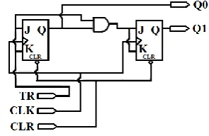
The State Anticipation Module consists of three D flip-flops, three 3-input AND gates and two inverters. It decodes the count states of basic counting module BCM. This decoding is carried over two clock cycles through two DFFs to trigger the second subsequent module, SCM2. In Figure 1, the first row consisting of a D flip-flop, a 3-input AND gate and an inverter decodes the low-order state Q2Q1Q0 =110 and carries this decoding across one clock cycle and enables Q4Q3 =01 at module SCM1 on the next rising clock edge. The second row of the State Anticipation Module decodes the
[image:2.595.315.539.163.330.2]low-order state Q2Q1Q0 =101 and carries this decoding over two cycles. By Combining the one cycle action in the counting section for Q4Q3 =10 and a two-cycle action for Q2Q1Q0 =101, Q7Q6Q5 can be enabled. The propagation delay can be considerably reduced by this type of simultaneous triggering of all the modules. Figure 5 shows the measured waveforms of the High Speed Counter using Altera Quartus II simulator at 250MHz.
Fig 1: Functional block diagram of the proposed high speed parallel counter
Fig 2: The Schematic diagram of Module-BCM of the proposed high speed parallel counter
Fig 3: The Schematic diagram of Module- SCM1 of the
proposed high speed parallel counter
Q0(t+1) = 1 Q0(t) (1)
Q1(t+1) = Q0(t) Q1(t) (2)
Q2(t+1)=[Q1(t)Q0(t)] Q2(t) (3)
Q0(t+1)= TR Q0 (t) (4)
Q1(t+1)= [TR Q0(t )] Q1(t) (5) Q0(t+1)= TR Q0(t) (6)
Q1(t+1)= [TRQ0(t )] Q1(t) (7)
[image:2.595.351.499.520.616.2]Fig 4: The Schematic diagram of Module-SCM2 of the proposed high speed parallel counter
Fig 5: Measured waveforms of the proposed High Speed Counter using Altera Quartus II simulator at 250MHz
3.
THE PROPOSED PROGRAMMABLE
SQUARE FINDER CUM FREQUENCY
DIVIDER
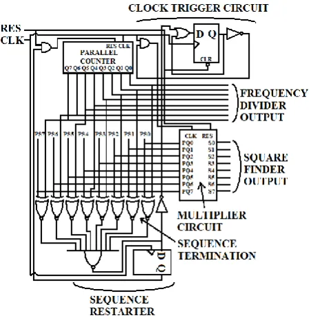
The programmable square finder cum frequency divider architecture proposed here is structured with a high speed parallel counter, clock trigger circuit, eight bit multiplier logic, sequence termination logic and sequence restarter logic. Figure 6 shows the Functional block diagram of the proposed programmable 8bit square finder cum frequency divider architecture. The frequency divider section of the proposed architecture consists of a counter, a sequence restarter and sequence termination logic with external programmable inputs for frequency select. The 8bit counter in conjunction with the sequence restarter and the sequence termination logic forms the frequency divider circuit. The sequence restarter circuit consists of a DFF and an AND gate. The 8bit counter in conjunction with the 8bit multiplier logic forms the square finder circuit.
Fig 6: Functional block diagram of the proposed programmable 8bit square finder cum frequency divider architecture
3.1
The frequency divider section
The frequency divider section consists of a high speed parallel counter, sequence restarter logic and a sequence termination detector with external programmable inputs PS7PS6PS5PS4PS3PS2PS1PS0 for frequency select. The sequence termination detector is a comparator, which is designed to detect the desired frequency-divide-by-N. The XNOR logic gates are used here for comparing bits which outputs a logic level „HIGH‟ when both of its input bits are equal. The output of the NAND gate will remain at logic level „HIGH‟ until the counter output combination „Q7Q6Q5Q4Q3Q2Q1Q0‟ becomes equal to external input pattern „PS7PS6PS5PS4PS3PS2PS1PS0‟.When counter output „Q7Q6Q5Q4Q3Q2Q1Q0‟ becomes equal to „PS7PS6PS5PS4PS3PS2PS1PS0‟ the output of the NAND gate switches to logic level „LOW‟. The output of the NAND gate acts as the input to the sequence restarter logic which consists of a DFF and an AND gate. So whenever the counter output matches with the external input combination the output of all the XNOR gates becomes „1‟(logic level „HIGH‟) which results in a logic level „LOW‟ at the NAND gate output. At the leading edge of the next clock pulse this logic value will be transferred to the DFF „Q‟ output which causes the output of the two input AND gate to switch from logic level „HIGH‟ to „LOW‟ and causes the counter to enter into RESET state thereby restarting the counting cycle before entering through all the possible state allowed by the 8bit combination.
[image:3.595.57.278.73.176.2] [image:3.595.53.282.209.381.2]input combination provides the option of selecting any 8bit modulus value possible with an 8bit pattern.
3.2
The square finder section
The square finder section consists of a high speed parallel counter architecture, a clock trigger circuit, and a multiplier circuit with external programmable inputs PS7PS6PS5PS4PS3PS2PS1PS0 for the selection of the number whose square has to be calculated. It can be noted that both the square finder and frequency divider circuits share the same parallel counter circuit for their operation. Both the circuits also share the same set of external programmable select inputs. The clock trigger circuit consists of a DFF, an OR gate, an AND gate and a NOT gate. The AND gate output acts as the clock trigger pulse to the multiplier circuit.
Fig 7: The 8bit multiplier logic circuit
Figure 7 shows the schematic diagram of the 8bit multiplier logic circuit. It consists of an 8bit adder and nine DFFs. The output Q of the first DFF on the top left hand side is used to provide value to the asynchronous „CLEAR‟ input of the remaining 8 flip flops. The upper flip-flop ensures a single flip-flop delay between the application of logic „HIGH‟ to RES input and CLEAR input of the remaining flip-flops which is necessary for the proper working of this particular circuit design. The external select bit combination is permanently assigned to the bit combination A7A6A5A4A3A2A1A0 of the adder.
The second bit combination B7B6B5B4B3B2B1B0 has an initial value of „00000000‟ since initially all the bottom 8 flip-flops are at RESET state. The result of the addition process produces a bit combination S7S6S5S4S3S2S1S0 which acts as the input to the 8 flip-flops in a row. Before the leading edge of the first clock pulse the output of the adder will be A7A6A5A4A3A2A1A0 since, B7B6B5B4B3B2B1B0 was initially „00000000‟. After the leading edge of the first clock pulse, B7B6B5B4B3B2B1B0 takes the previous value of S7S6S5S4S3S2S1S0. This process gets repeated for the next coming clock leading edges and finally produces an output which is exactly the binary pattern of the square of the given number entered in binary pattern through the external programmable select input as shown in Figure 8. It can be generalized for any given input for this particular circuit that it produces the desired result only after a delay of (m+1) clock cycles, where „m‟ is the decimal value of the given input. As an example, in Figure 8 the desired result was produced only after „7‟ clock pulses as the equivalent decimal value of the entered input binary pattern through the external programmable input was „6‟.The input pattern is marked by a
small circle whereas the output pattern is marked by a bigger circle.
Fig 8: Measured waveforms of the proposed programmable square finder cum frequency divider architecture for an external input combination ‘00000110’ using Altera Quartus II simulator at 250MHz.
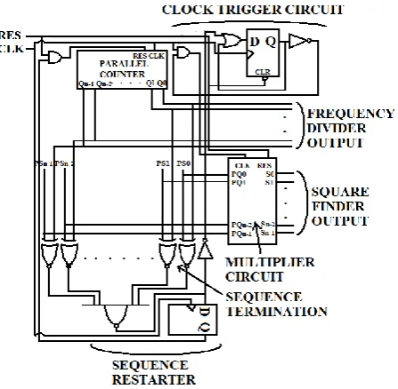
[image:4.595.317.539.99.244.2]Fig 9: Functional block diagram of the proposed programmable n-bit square finder cum frequency divider architecture.
[image:4.595.55.279.240.386.2] [image:4.595.318.542.310.529.2] [image:4.595.316.541.578.708.2]Figure 9 shows the Functional block diagram of the proposed programmable n-bit square finder cum frequency divider architecture. One main problem encountered here is that as the number of bits of the counter increases the number of logic gates and thereby the number of transistors required increases which results in more area and power consumption. Figure 10 shows the schematic diagram of the n-bit multiplier logic circuit. It consists of an n-bit adder and (n+1) DFFs. The output Q of the first DFF on the top left hand side is used to provide value to the asynchronous „CLEAR‟ input of the remaining n flip flops. When CLEAR=‟0‟, all the flip-flops will be at RESET state. For normal operation, CLEAR input of the flip-flop should be equal to „1‟.
4.
RESULTS AND DISCUSSIONS
The performance analysis of the proposed high-speed low power parallel 8-bit counter architecture and the programmable square finder cum frequency divider architectures is provided in this section
4.1
Proposed Parallel Counter architecture
In this section the performance of the proposed high-speed low power parallel 8-bit counter architecture is analyzed first and is compared with the existing parallel counter architecture. Note that for all the observations the device cyclone EP1C20F400C7 is used here. The Power dissipation of the counter at 250 MHz was found to be 3.54 mW(PINT)
and the delay was 7.481ns for the existing high speed parallel counter[5] using Altera Quartus II simulator. The Power dissipation of the counter at 250 MHz was found to be 2.91mW(PINT) and the delay was 6.737ns for the proposed
high speed parallel counter using Altera Quartus II simulator. Table I shows that a reduction in area(transistor count) by 38% and a reduction in power dissipation by 17.80% is achieved for the proposed counter architecture compared to the existing work by S. Abdel-Hafeez et al.[5]. A reduction in delay by 9.95% is achieved for the proposed method compared to the existing work. When compared with existing Digital Parallel counter [5], the proposed Parallel counter shows improved performance in terms of power consumed,
delay and area. Compared to the conventional 8-bit synchronous counter using JK flip-flops a reduction in delay by 22.10% is achieved for the proposed high speed parallel counter.
4.2
Proposed square finder cum frequency
divider architectures
In this section the performance of the proposed programmable square finder cum frequency divider architectures using the existing and proposed counter architectures are analyzed.
4.2.1
Proposed square finder cum frequency
divider architecture using existing counter
architecture [5]
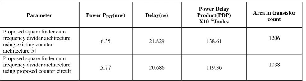
The total transistor count of the Proposed square finder cum frequency divider architecture using existing counter circuit [5] is 1206 in which the transistor count of the counter, sequence termination logic, sequence restarter logic, multiplier circuit and clock trigger circuit are 442, 144, 24,562 and 34 respectively. A worst case delay of 21.829ns was measured from clock to destination pin S4 of the square finder section for the proposed programmable square finder cum frequency divider architecture using existing counter circuit. The Power dissipation at 250 MHz was found to be 6.35 mW(PINT).
4.2.2
Proposed square finder cum frequency
divider architecture using proposed counter
circuit.
[image:5.595.54.538.557.733.2]The total transistor count of the proposed square finder cum frequency divider architecture using proposed counter circuit is 1038 in which the transistor count of the counter,sequence termination logic, sequence restarter logic, Multiplier Circuit and Clock Trigger Circuit are 274, 144, 24,562 and 34 respectively. Thus a reduction area(transistor count) of 13.93% is achieved for the proposed programmable square finder cum frequency divider architecture using proposed counter circuit compared to the same using existing counter circuit.
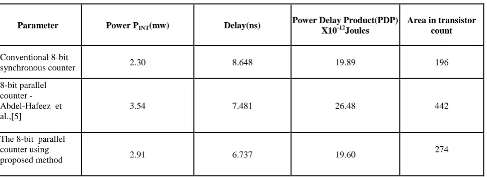
Table 1. Comparison of performance of parallel counter architectures
Parameter Power PINT(mw) Delay(ns)
Power Delay Product(PDP) X10-12Joules
Area in transistor count
Conventional 8-bit
synchronous counter 2.30 8.648 19.89 196
8-bit parallel counter - Abdel-Hafeez et al.,[5]
3.54 7.481 26.48 442
The 8-bit parallel counter using
proposed method 2.91 6.737 19.60
Table 2. Comparison of performance of square finder cum frequency divider architectures
A worst case delay of 20.686ns was measured from clock to destination pin S2 of the square finder section for the proposed programmable square finder cum frequency divider architecture. Thus a reduction in delay of 5.24% is achieved for the proposed programmable square finder cum frequency divider architecture using proposed counter circuit compared to the same using existing counter circuit. The Power dissipation at 250 MHz was found to be 5.77mW(PINT)
resulting a reduction in power by 9.13% for the proposed programmable square finder cum frequency divider architecture using proposed counter circuit compared to the same using existing counter circuit.
5.
CONCLUSION
In this paper, an 8-bit programmable square finder cum frequency divider architecture is presented. An innovative parallel counter design that speeds up the operation of the square finder cum frequency divider circuit is also presented. The AND gate rippling that results in reduction in speed in conventional counters has been eliminated by the proposed counter methodology. The tabulated results demonstrate the better performance of the proposed parallel counter in terms of delay and area compared to previous works. A reduction in area (transistor count) by 38% and a reduction in delay by 9.95% is achieved for the proposed high speed parallel counter compared to the existing parallel counter. This suggests its suitability for high speed arithmetic applications. The 8-bit programmable square finder cum frequency divider architecture is divided into two parts: The frequency divider section and the square finder section. The divider structure provides varied frequency dividing factors from 2 to 255. The square finder cum frequency divider circuit employing the proposed counter consumes a total transistor count of only 1038 as against 1206 consumed by the same circuit employing existing parallel counter. The worst case delay of the proposed programmable square finder cum frequency divider architecture employing the existing and proposed counter architecture was found to be 21.829ns and 20.686ns respectively and the Power dissipation at 250 MHz was found to be 6.35 mW and 5.77mW respectively.
6.
REFERENCES
[1] Chu, D. “Phase digitizing sharpens timing measurements,” IEEE Spect., pp. 28-32, July 1988 [2] Yuan, J.R. “Efficient CMOS Counter Circuits,”
Electronics Letters,vol. 24, pp. 1,311-1,313, Oct. 1988. [3] Yuan, J.R. and Svensson, C. “Fast CMOS Nonbinary
Divider and Counter,” Electronics Letters, vol. 29, pp. 1,222-1,223, June 1993.
[4] Rogenmoser, R., Huang, Q and Piazza, F “1.57 GHz Asynchronous and 1.4 GHz Dual-Modulus 1.2 mm CMOS Prescalers,” Proc. Custom Integrated Circuits Conf., pp. 387-390, May 1994.
[5] Abdel Hafeez, S and Ann Gordon Ross,“A Digital CMOS Parallel Counter Architecture Based on State Look-Ahead Logic”, IEEE Transactions on Very Large Scale Integration(VLSI) Systems, vol.19, no. June2011 [6] Abdel-Hafeez, S Harb.S, and Eisenstadt.W, “High speed
digital CMOS divide-by-N frequency divider,” in Proc. IEEE Int. Symp. Circuits Syst., pp. 592–595,2008 [7] Alioto, M. Mita. R, and Palumbo. G,“Design of
high-speed power-efficient MOS current-mode logic frequency dividers,” IEEE Trans. Circuits Syst. II, Expr. Briefs, vol. 53, no. 11, pp. 1165–1169, 2006
[8] Chang, B Park. J, and Kim. W, “A 1.2 GHz CMOS dual-modulus prescalar using new dynamic D-type flip-flops,” IEEE J. Solid-State Circuits, vol. 31, no. 5, pp. 749–75, 1996
[9] Hendry. D. C, “Sequential lookahead method for digital counters,” IEEE Electron. Lett., vol. 32, no. 3, pp. 160– 161,1996.
[10] Kakarountas, A.P., Theodoridis, G., Papadomanolakis K. S. and C. E. Goutis, “A novel high-speed counter with counting rate independent of the counter‟s length,” in Proc. IEEE Int. Conf. Electron., Circuits Syst. (ICECS), UAE, Dec. 2003, pp. 1164–1167
[11] Altera Corp., Santa Clara, CA, “FLEX8000, field programmable gate array logic device,” 2008.
[12] Stan, M. R., “Systolic counters with unique zero state,” in Proc. IEEE Proc. Int. Symp. Circuits Syst. (ISCAS), 2004, pp. II-909–II-912.
[13] Yamamoto, K and Fujishima, M, “4.3 GHz 44 uW CMOS frequency divider,” in Proc. IEEE Int. Solid-State Circuits Conf., 2004, pp.104–105.
[14] Alioto, M. and Palumbo, G., “Model and Design of Bipolar and MOSCurrent-Mode Logic: CML, ECL and SCL Digital Circuits”. Norwell,MA: Springer-Verlag, 2005.
Parameter Power PINT(mw) Delay(ns)
Power Delay Product(PDP)
X10-12Joules
Area in transistor count
Proposed square finder cum frequency divider architecture using existing counter architecture[5]
6.35 21.829 138.61 1206
Proposed square finder cum frequency divider architecture
using proposed counter circuit 5.77 20.686 119.36