Abstract—A physical micromachining technique is demon-strated in a low-loss flat-fiber substrate to fabricate a multi-mode interference (MMI) device. The flat-fiber substrate is a low-index-contrast material; however, by making use of two phys-ically micromachined trenches, lateral confinement is achieved providing high index contrast for the MMI region. A 1 3 MMI device exhibiting 1.89 dB of excess loss has been demonstrated.
Index Terms—Air trenches, flat fiber, multimode interference (MMI).
I. INTRODUCTION
M
ULTIMODE INTERFERENCE (MMI) devices have attracted interest in integrated optics owing to their widespread benefits such as small device dimensions and a broad spectral bandwidth [1]. MMI devices have been success-fully demonstrated in a wide range of applications, particularly for power splitting and combining purposes. Recently, they have been proposed for more active applications, including optical sensing [2] and switching [3]. The device structure has been extensively demonstrated in both low- and high-index-contrast materials, for example, silica-on-silicon [4], polymer [5], and silicon-on-insulator [6] platforms; yet, most of these materials are either relatively expensive, have low index contrast, exhibit high loss, or have complex fabrication processes. The study reported in this paper uses a novelflatfiber [7], [8] to fabricate an MMI structure. This platform has the benefits of being relatively inexpensive, yielding a low insertion loss and being mechanicallyflexible compared to traditional planar platforms.Manuscript received January 16, 2012; revised March 21, 2012; accepted May 07, 2012. Date of publication May 15, 2012; date of current version August 17, 2012. This work was supported in part by the University of Southampton, Ministry of Higher Education High Impact Research Grant (Integrated Pho-tonics for Biosensors), Malaysia, and the University of Technology Malaysia.
S. Ambran is with the Optoelectronics Research Center, University of Southampton, SO17 1BJ, U.K., and also with the Malaysia–Japan International Institute of Technology, University Technology of Malaysia, Kuala Lumpur, Malaysia (e-mail: [email protected]).
C. Holmes, J. C. Gates, A. S. Webb, L. G. Carpenter, P. G. R. Smith, and J. K. Sahu are with the Optoelectronics Research Center, University of Southampton, SO17 1BJ, U.K. (e-mail: [email protected]; [email protected]; asw@orc. soton.ac.uk; [email protected]; [email protected]; [email protected]. uk).
F. R. M. Adikan is with the Department of Electrical Engineering, University of Malaya, Kuala Lumpur, Malaysia (e-mail: [email protected]).
Color versions of one or more of thefigures in this paper are available online at http://ieeexplore.ieee.org.
Digital Object Identifier 10.1109/JLT.2012.2199465
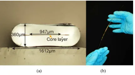
Fig. 1. (a) Cross section and (b) bending of theflatfiber. The index contrast of the germanium-doped core and the cladding of theflatfiber is 0.0183.
In addition, the physical micromachining technique reported provides the advantages of high-index-contrast design.
Flatfiber has a similar fabrication technique as standard op-ticalfiber, using modified chemical vapor deposition (MCVD) andfiber drawing processes to lead to a low-cost planar sub-strate [7]. The process differs from the standardfiber fabrica-tion during the collapse of the preform. This occurs at thefiber drawing stage, where a vacuum is applied to flatten the pre-form into a planar geometry. Fig. 1(a) shows the cross sec-tion and (b) the bending of a length of flatfiber showing its geometry and flexibility. In the context of conventional MMI devices, theflat-fiber platform would typically be considered a low-index-contrast material. Such low-index-contrast systems lead to lower optical confinement and, thus, reduced perfor-mance of the resulting MMI device [9]. However, it does have the benefit of providing low coupling loss, with standard silica opticalfibers. This is due to better mode matching, compared to that of high-index-contrast platforms, and a comparable refrac-tive index tofiber unlike materials such as silicon.
In this study, we combine the benefits associated with low-and high-index-contrast materials. The low index contrast is
de-fined vertically, provided by a germanium (Ge)-doped core layer sandwiched by a top and bottom cladding layer of theflatfiber. In our devices, the high index con-trast is formed horizontally between air trenches and the core layer as illustrated in Fig. 2.
In the past, various techniques have been used to form high-index-contrast MMI structures. For example, one of the reported techniques used metal-clad sidewalls, where the waveguide sur-face was surrounded by a thin metal layer. This acts to increase the index contrast of the MMI device. However, this technique is
[image:1.592.323.538.201.321.2]Fig. 2. 3-D schematic diagram of the micromachined trenches in theflat-fiber substrate. Two trenches were cut parallel to the MMI section to define the region of light confinements.
limited to operating with one polarization only as the TE cannot be supported within the waveguide [10]. The concept presented in this paper uses a similar concept to previous work [9], [11], where air trenches are used to define a large index contrast of the MMI section. In general, such an approach affords strong lateral confinement, and with it, good imaging performance [12] and coupling efficiency [9].
Several fabrication techniques have previously been reported to produce such high-index lateral confinement of the MMI de-vice. Photolithography followed by etching is the conventional fabrication technique and has been widely used in many inte-grated optical applications [9], [13]. However, these cleanroom techniques can be time consuming, and require several stages to complete a device. This paper presents an alternative fab-rication technique employing physical micromachining of the
flat-fiber substrate to form the MMI section using air trenches. The novelty behind this study is that it combines physical micro-machining with a low-costflat-fiber fabrication platform. Fur-thermore, with theflat-fiber format, it is difficult to use lithog-raphy and etching simply because of the difficulty of spinning photoresists on such a geometry. The technique used here offers a simple and straightforward fabrication approach where a dia-mond-blade dicing saw is used to physically machine a pair of trenches, as illustrated in Fig. 2. This micromachining method has been previously used to fabricate micro-optical mechanical systems [14].
This paper is structuredfirst to detail the theoretical modeling of the MMI device. The concept of the micromachined trenches is described in Section II. The technique used to fabricate the MMI device is explained in Section III. In Section IV, we elab-orate on the characterization setup used to measure the perfor-mance of the device. Finally, Section V contains experimental results and a discussion and Section VI concludes this paper.
II. DESIGN ANDCONCEPT
[image:2.592.51.281.66.194.2]Self-imaging is a key concept for MMI device operation where a single transverse optical mode at the input of the device can be reproduced as a single or multimode image at certain positions along it. The self-imaging operation of an MMI device primarily depends on three parameters, the effective width , the effective refractive index , and the
Fig. 3. BeamPROP modeling of the propagation light within the MMI section. Single-mode light is launched into the center of the MMI section, and three output spots are produced at the output section. The wavelength of 1652 nm was implemented in the modeling.
operation wavelength , where the length of the device is given by (1) [15]
(1) Fig. 2 shows the 3-D schematic diagram of the MMI device, where two micromachined trenches were physically machined to form an MMI section. These trenches form a high-index inter-face and thus give lateral confinement for both sides of the MMI region. The vertical confinement is achieved by the flat-fiber core layer having a higher refractive index than the cladding and is due to germanium doping.
As way of demonstration, we designed an MMI device as a 1 3 splitter, where the trenches confine the light to regenerate the input mode at three individual locations at the output facet. The MMI structure has been modeled using commercial Beam-PROP software from the Rsoft design group in order to pre-dict the dimensions of the MMI structure as well as determine the effect of certain parameters. In the modeled system, the slab waveguide mode, in they-axis, had an effective index of 1.4592 at 1652 nm; this reduces the problem to two dimensions [15]. A Gaussian mode was selected as the launched light parameter with a mode-field diameter (MFD) of 10.5 m to represent the polarization maintaining (PM)fiber used in the measurement setup. The light propagation pattern throughout the MMI wave-guide is shown in Fig. 3 for the specific case of a 1 3 MMI device.
III. MMI DEVICEFABRICATION
Fig. 4. Schematic diagram illustrating how the dicing machine is used to fab-ricate the MMI air trenches. The substrate is translated in thez-direction where the dicing is made to cut the core layer section laterally.
in-line with the expected value for the core glass based upon the known doping parameters of the MCVDfiber process. Two trenches were physically cut using an ultraprecision dicing saw with a 5000 grit nickel-bonded diamond blade as depicted in Fig. 4. The overcladding of theflatfiber was removed via lap-ping to within about 100 m of the core layer. This reduced the total depth of the trench cuts and allowed sawing into the core layer using the blades available. The depth and the width of the trenches were 140 and 18 m, respectively. These saw cuts define the width of the MMI device and were measured postfabrication as 204 m. For this proof-of-principle device, an MMI width of 204 m was chosen to provide sufficient output channel spacing to assist in the analysis of the output via stan-dardfibers. A future optimized device would have to consider the design constraints associated with MMI width minimiza-tion [16] and the output coupling. The length of the device was predicted using BeamPROP modeling, which was 12.54 mm long. The end facet and hence the length of the device was ma-chined by the same dicing saw used to machine the trenches and hence had similar fabrication errors. These dimensions are optimized for the 1 3 splitting of laser light at 1652 nm. The operating wavelength is dominated by the precision of the mi-cromachining, the width of the MMI being the most sensitive dimension. The micromachining system used in this study has a blade positional error of 2 m and a blade width error of 2 m. In commercial dicing machines, these tolerances can be greatly reduced to submicrometer dimensions. Fig. 5(a) shows the end facet of the MMI section after micromachining, the trenches run parallel to the MMI section. A top view of the scanning electron microscope (SEM) image is depicted in Fig. 5(b). Although this does not provide a direct measurement of the width of the core layer, it shows that the micromachining technique yields very small wedge variation of the MMI section. Analysis via imaging white light interferometry (ZeScope made by Zemetrics) indi-cates width variation of less than 0.5 m over the 12.24 mm length of the device.
IV. CHARACTERIZATION
To observe the modal output from the device light, a tun-able laser source was launched into the middle of the MMI sec-tion via a PMfiber as depicted in Fig. 6. The output mode
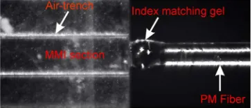
[image:3.592.314.545.62.222.2]pat-Fig. 5. (a) Microscope image of the end facet of the MMI section and (b) Top view of the SEM image showing the parallel characteristics along the MMI length. Two trenches were cut allowing the core layer being exposed to the air, providing a high index contrast between the refractive index of the core layer and the air trenches.
Fig. 6. Coupling image between the MMI section and the PMfiber.
tern was observed using a near infrared (NIR) camera. Due to the restricted range of the tunable laser, this was measured at 1641 nm which is close to the optimal operating wavelength of 1652 nm. A 20x objective was located between the end facet of the MMI device and the NIR camera. Due to the low dynamic range of the NIR camera, an alternative method to record the device operation used afiber that was directly butt coupled to the output of the MMI and translated to sample the optical in-tensity at the output facet. A PMfiber was used in order to main-tain the light polarization, and the coupled power was measured using a power meter. The measurements were made using TM polarization.
To investigate the wavelength dependence of the device, a spontaneous LED broadband light source (1610–1675 nm) was coupled into the device and the spectrum from each output was collected with an opticalfiber. The collected light was analyzed using an optical spectrum analyzer (ANDO AQ 6317B).
V. RESULTS ANDDISCUSSION
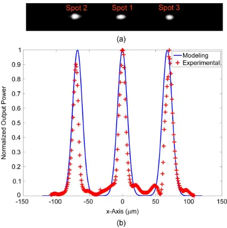
The modal image of the three output spots recorded by the NIR camera is shown in Fig. 7(a). The simulated and experi-mental results of the output intensity distribution can be seen in Fig. 7(b). The simulation result has been convoluted with a Gaussian mode profile with MFD of 10.5 m to represent the PMfiber that is used for scanning the MMI output facet. Mod-eling of the spectral dependence was also implemented to ob-serve the output peak power as a function of wavelength.
[image:3.592.339.521.291.369.2]Fig. 7. (a) Modal image of the 1 3 MMI device recorded by the NIR camera at 1641 nm and (b) quantitative optical output of the modal image via scanning measurement technique at the end facet of the MMI region using the PMfiber. The scanning is implemented horizontally along the width of the MMI section.
powers from each spot are strongly dependent on the wave-length of the light coupled into the MMI. Also, the optimum wavelength, i.e., lowest insertion loss, of the three spots is very similar. The output from spot 3 shows a small oscillation that we believe is due to a slight cavity formed between the MMI device andfiber connection. From the measurement, it shows that the optimum wavelength for the device was 1652 nm with the total excess loss of 1.89 dB. The total excess loss of the de-vice was calculated by taking the ratio between the launched power into the sample and the sum of the three peak outputs. It is worth noting that the most equal splitting ratio occurs at 1620 nm but this is outside the 1 dB bandwidth as described here. From Fig. 8, wefind that the bandwidth of minimum excess loss, less than 1 dB increase, spans from 1636 to 1673 nm cor-responding to a width of 37 nm. This can be compared to recent reports of photonic-crystal-based beam splitters demonstrating a 1 dB bandwidth of 11 nm in theC-band [17]. Over this spec-tral bandwidth, the uniformity of the outputs is 1.24 dB which is comparable to current commercially available devices. Fig. 9 shows the normalized transmission from the experiment data compared to the BPM model, as a function of wavelength. The results agree within the wavelength range of 1635–1660 nm. Outside this spectral range, a small disagreement between the modeling and experimental result can be seen from the graph. The discrepancy between the experimental data and the model is due to the dispersion, as this was not been taken into consid-eration when modeling the MMI device.
[image:4.592.52.274.61.284.2]There are three main contributions associated with the total excess loss of the experimental result. They are propagation loss, coupling loss, and scatter loss. In a preliminary experi-ment, the propagation loss of theflatfiber was measured via two different measurement methods at 1550 nm wavelength. These were a Bragg grating loss measurement technique [18] and a measurement using an optical backscattered reflectometer
Fig. 8. Insertion loss from each of the three output spots against the wave-length. The total excess loss is also calculated by summing all three output powers at each respective wavelength.
Fig. 9. Normalized transmission from the modeling represented as solid line, showing good agreement to the experimental data. The optimum wavelength of the maximum point is 1652 nm.
(OBR) model 4400 from Luna technology system. The mea-sured loss of theflatfiber was dB/cm for the Bragg grating loss measurement and dB/cm for the OBR system. These two different measurements show good agree-ment and also concur with that observed with previous samples [7]. Even though the number provided here is the propagation loss specifically for UV-written channel waveguides, it is used as an estimation of the anticipated upper bound for the intrinsic propagation loss within theflat-fiber material. This estimation of propagation loss includes the material loss and scatter loss from cladding and core layers. It does not include the scatter loss from the trench sidewalls, which is discussed later.
[image:4.592.311.543.61.236.2] [image:4.592.308.547.287.462.2]also changes the MMI properties making it difficult to make quantitative measurements. However, we believe the scattering loss of the device is small as no significant effect in term of the device performance was observed after an index oil of 1.33 was placed within the trenches.
The excess loss measured here (1.89 dB) is still higher than expected from the modeling results. Removing the known losses in the system, i.e., the propagation loss and thefiber coupling losses, an additional loss of 0.57 dB remains. This higher loss is expected to be associated with factors that the modeling does not account for, such as the scattering loss due to the surface roughness and a possible lack of verticality of the trench side-walls. This magnitude of loss is comparable to other reported work using conventional fabrication techniques [19]–[21].
VI. CONCLUSION
We have demonstrated for the first time a 1 3 MMI de-vice fabricated by physical micromachining channels in a low-loss flat-fiber substrate. Although the flat-fiber substrate is a low-index-contrast platform, by using two air trenches, a high-index lateral contrast can be produced to achieve better output imaging. The MMI device has 1.89 dB excess loss, which was attributed to fabrication imperfection and scatter loss. Such components could be integrated into longerflat-fiber lengths and combined with previously published UV writing technology [7] for splitting and combining operations.
REFERENCES
[1] L. B. Soldano and E. C. M. Penning, “Optical multi-mode interference devices based on self-imaging: Principles and application,”J. Lightw. Technol., vol. 13, no. 4, pp. 615–627, Apr. 1995.
[2] M. Mayeh, J. Viegas, P. Srinivasan, P. Marques, J. L. Santos, E. G. Johnson, and F. Farahi, “Design and fabrication of slotted multimode interference devices for chemical and biological sensing,”J. Sensor, pp. 470175-1–470175-11, 2009.
[3] Z. Jin, C. J. Kaalund, and G. Peng, “Novel approach to design high performance large-port-count switches in low-index-contrast materials based on cascaded multimode interference couplers,”IEEE J. Quantum Electron., vol. 41, no. 12, pp. 1548–1551, Dec. 2005.
[4] C. Holmes, H. E. Major, J. C. Gates, C. B. E. Gawith, and P. G. R. Smith, “Period adapted Bragg mirror multimode interference device,” inProc. Conf. Lasers Electro-Opt./Quantum Electron. Laser Sci. Conf., 2009, pp. 1–2.
[5] M. H. Ibrahim, N. M. Kassim, A. B. Mohammad, M. K. Chin, and S. Y. Lee, “Multimode interference optical splitter based on photodefinable benzocyclobutene (BCB 4024-40) polymer,”Opt. Eng., vol. 46, no. 1, pp. 013401-1–013401-4, 2007.
[6] H. Chen and D. T. K. Tong, “Two-dimensional symmetric multimode interferences in silicon square waveguide,”IEEE Photon. Technol. Lett., vol. 17, no. 4, pp. 801–803, Apr. 2005.
[7] A. S. Webb, F. R. M. Adikan, J. K. Sahu, R. J. Standish, C. B. E. Gawith, J. C. Gates, P. G. R. Smith, and D. N. Payne, “MCVD planar substrates for UV-written waveguide devices,”Electron. Lett., vol. 43, no. 9, pp. 517–519, 2007.
[12] M. K. Chin, C. W. Lee, S. Y. Lee, and S. Darmawan, “High-index-con-trast waveguides and devices,” Appl. Opt., vol. 44, no. 15, pp. 3077–3086, 2005.
[13] Y. Ma, S. P. L. Wang, and S. T. Ho, “Ultracompact multimode in-terference 3-dB coupler with strong lateral confinement by deep dry etching,”IEEE Photon. Technol. Lett., vol. 12, no. 5, pp. 492–494, May 2000.
[14] L. G. Carpenter, C. Holmes, H. L. Rogers, P. G. R. Smith, and J. C. Gates, “Integrated optic glass microcantilevers with Bragg grating in-terrogation,”Opt. Exp., vol. 18, no. 22, pp. 23296–23301, 2010. [15] K. Okamoto, “Fundamentals of Optical Waveguides,” inMultimode
Interference (MMI) Device, 2nd ed. New York: Academic, 2006, pp. 46–55.
[16] A. Hosseini, H. Subbaraman, D. Kwong, Y. Zhang, and R. T. Chen,
“Optimum access waveguide width for 1 N multimode interference
couplers on silicon nanomembrane,”Opt. Lett., vol. 35, no. 17, pp. 2864–2866, 2010.
[17] M. Zhang, R. Malureanu, A. C. Kruger, and M. Kristensen, “1 3
beam splitter for TE polarization based on self-imaging phenomena in photonic crystal waveguides,” Opt. Exp., vol. 18, no. 14, pp. 14944–14949, 2010.
[18] H. L. Rogers, S. Ambran, C. Holmes, P. G. R. Smith, and J. C. Gates, “In situ loss measurement of direct UV written waveguides using in-tegrated Bragg gratings,”Opt. Lett., vol. 35, no. 17, pp. 2849–2851, 2010.
[19] M. Bruendel and D. G. Rabus, “1 2 and 1 3 multimode interference couplers fabricated by hot embossing and DUV-induced modification of polymers,” inProc. 19th Annu. Meet. IEEE Conf. Lasers Electro-Opt. Soc., 2006, pp. 326–327.
[20] P. A. Besse, E. Gini, M. Bachmann, and H. Melchior, “New 2 2 and 1 3 multimode interference couplers with free selection of power splitting ratios,”J. Lightw. Technol., vol. 14, no. 10, pp. 2286–2293, Oct. 1996.
[21] J. M. Hong, H. H. Ryu, S. Y. Park, J. W. Jeong, S. G. Lee, E.-H. Lee, S.-G. Park, D. Woo, S. Kim, and O. Beom-Hoan, “Design and fabri-cation of a significantly shortened multimode interference coupler for polarization splitter application,”IEEE Photon. Technol. Lett., vol. 15, no. 1, pp. 72–74, Jan. 2003.
Sumiaty Ambranreceived the B.S. degree in electronics telecommunication from the University Technology of Malaysia, Johor, Malaysia, in 2005, and the Master’s degree from the University of MARA, Selangor, Malaysia, in 2008. She is currently working toward the Ph.D. degree in Silicafiber Fabrication and Planar Optical Materials Group, Optoelectronics Research Centre, University of Southampton, Southampton, U.K.
She is currently involved in the development of UV-writtenflat-fiber sub-strate for planar optical devices. She is also with the Malaysia–Japan Interna-tional Institute of Technology, University Technology of Malaysia, Johor. Her research interests include rare-earth-doped optical devices for laser and ampli-fier application.
Ms. Ambran is a member of the Optical Society of America.
Christopher Holmesreceived the M.S. degree (first-class hons.) in physics from Warwick University, Coventry, U.K., in 2004, and the Ph.D. degree in direct UV-written devices from the University of Southampton, Southampton, U.K., in 2009.
James C. Gates received the M.Phys. degree from the University of Southampton, Southampton, U.K., in 1999, where he also received the Ph.D. degree from the Optoelectronics Research Centre (ORC), in 2003.
He is currently a Senior Research Fellow at the ORC. His Ph.D. thesis investigated the optical properties of various photonic devices at a nanometer scale using an interferometric near-field technique. He was involved in research in thefield of nanophotonics in the Department of Physics, University of Southampton, before returning to the ORC in 2006. He is currently involved in the development of planar-integrated optical devices for a wide range of applications in telecommunications and detection.
Andrew S. Webbreceived the B.Sc. degree in physics and electronics from Keele University, Staffordshire, U.K., in 1998. He is currently working toward the Ph.D. degree at the University of Southampton, Southampton, U.K.
In 2001, he became a Silica Fiber Fabrication Engineer at the Optoelectronics Research Centre, University of Southampton. He has coauthored more than 30 publications and patents. His current research interests include developing novel modified chemical vapor deposition rare-earth-doped preform fabrication tech-niques, opticalfiber drawing, and production of specialty opticalfibers.
Mr. Webb is a member of the Institute of Engineering and Technology, a member of the Institute of Physics, and a student member of the Optical Society of America.
Lewis G. Carpenterreceived the B.E. degree (withfirst class) in electrical engineering from the University of Southampton, Southampton, U.K., in 2009. He is a Postgraduate Research Student at the Optoelectronics Research Centre, University of Southampton. His current studies explore physical micromachining techniques for integrated optics and micro-opto-mechanical systems.
Mr. Carpenter is the recipient of the National Grid Award for his dissertation.
Faisal Rafiq Mahamd Adikanreceived the Ph.D. degree from the Optoelec-tronics Research Centre, University of Southampton, Southampton, U.K., in 2007.
He is currently the Head of the Photonic Lightwave Circuit Group, Photonics Research Centre, University of Malaya, Kuala Lumpur, Malaysia, where he is involved in developing novel fabrication processes to incorporate optically ac-tive materials into a glass matrix. His Ph.D. research onflatfiber produced an international patent. He specializes in glass-based integrated optical devices for use in telecommunication and sensing applications. Apart from research and teaching, he is also an active member of his Faculty, holding a number of ad-ministrative posts including the Coordinator of the Telecommunication Engi-neering program. He has published more than 70 journal and conference papers on optics and engineering education. He was the Deputy Chair of two Technical Postgraduate Symposiums, and is the current Chairman for the Faculty of Engi-neering’s Sports and Recreational Club. He also established the Junior Lecturer Forum, an informal platform for young staff members to discuss matters con-cerning career development.
Dr. Rafiq was the recipient of the Section Prize for the Best Engineering Re-search during presentations at the House of Commons (British Parliament) in 2006. He also received the International Society for Optical Engineers Educa-tional Scholarship in optical science and engineering in 2004, and the Best Paper for Photonic Category during an international conference in 2003.
Peter G. R. Smithreceived the B.A. degree in physics and the D.Phil. degree in nonlinear optics from Oxford University, Oxford, U.K., in 1990 and 1993, respectively.
He is currently a Professor at the Optoelectronics Research Centre and in the Department of Electronics and Computer Science, University of Southampton. After a year spent as a Management Consultant, he joined the University of Southampton, where he currently leads a research group concentrating on the fabrication of optical devices using integrated optics technology, particularly on direct UV writing and precision machining of optical materials. He is also involved in research on periodic poling technology and nonlinear optics. He has more than 200 publications, 10 patents, and was the founder of two spin-outs from Southampton—Stratophase Ltd. in 2003 and Covesion Ltd., in 2009.
Jayanta K. Sahureceived the Ph.D. degree in physics from the India Institute of Technology Kharagpur, Kharagpur, India, in 1997.
From 1997 to April 2000, he was a Research Engineer at the Royal Institute of Technology, Stockholm, Sweden. In May 2000, he joined the Optoelectronics Research Centre, University of Southampton, Southampton, U.K., where he is currently a Principal Research Fellow and leading the Fiber Fabrication Group. He has published more than 250 papers in scientific journals and conference pro-ceedings, including many invited and postdeadline papers. His current research interests include optical materials, development of novel silica-basedfiber struc-tures, and cladding-pumped rare-earth-dopedfiber lasers and amplifiers.