Technology (IJRASET)
A 4-Dimensional Parity based Data Decoding
Scheme for EDAC in Communication Systems
Vijay Tawar#1, Rajani Gupta*2 #
Electronics and Communication Department, KNPCST, RGPV Bhopal, India
Abstract— The applications and use of hardware in wireless communication is increasing day by day. Portability of
systems with data integrity during communication is the basic need of the systems in communication technology. This is a great force for the development of low power systems architectures. The wireless communication medium has various signals that can affect the low power communication signals of any system. So in wireless systems that operate on low power signals a good technique of data encoding and decoding is always preferred to use to transmit data through the medium. An effective data decoder is capable of identifying the changes that are caused in the transmitted data in the communication path and also capable to correct the data. Such an encoding-decoding technique is called as Error Detection and Correction (EDAC) Coding Technique. One of such technique that is most commonly used in the communication systems is based on the concept of Parity Encoding and Decoding. In the proposed work a 4-dimensional parity based encoding-decoding algorithm is presented. In this algorithm the error detection and correction logic is implemented by calculating parity of a data set in a matrix arrangement. The parity is calculated in the directions: horizontal, vertical, forward diagonal and backward diagonal. This algorithm is a low-complex hardware implementation design of error detection and correction code. The present work presents the hardware resource utilization on Xilinx FPGA devices.
Keywords— EDAC Code, Even Parity Encoder, FPGA, Hardware Resource Utilization, HVD Parity, Odd Parity, Xilinx
I. INTRODUCTION
In the modern communication systems wireless technology is emerging as a potential part of the systems. With the development of user application devices the amount of data transfer is also increasing tremendously. The data transfer among user devices is also increasing due to freely available software based user applications. This offers a greater possibility of portability and system up-gradation with the advancing system technologies. The wireless systems are more likely to be affected by the reception of noise signals by the receiving system antenna due to presence of wide complex signals in the communication environment. So an effective error identification scheme is required by the systems that perform control operations by using the received signal information. A better technique over the error detection technique also performs the correction in the received data when an error is detected in it. The change in the received data can be checked at the receiver end by using the received information that was added by the transmitter in the original data prior to its transmission. This extra information data is called as redundant data. One of the technique that offers a low complex hardware for implementing an effective error detection and correction algorithm is a multi-dimensional parity based scheme. In the proposed work a four dimensional parity based scheme is implemented on Xilinx field programmable gate array device to analyse its performance for multiple bit error detection and correction. The paper is organized as follows: Section-II presents the previous work review. Section-III presents the working of the proposed encoder and decoder with the help of the flow chart of the encoder and decoder. Section-IV presents the experimental and simulation results of the proposed encoder and the decoder with the help of waveform simulation diagram. Hardware utilization of the proposed design on Xilinx FPGA device is also summarized in Section-IV. Section-V presents the conclusion of the proposed work. Acknowledgement and References are presented after Section-V.
II. PREVIOUSWORK
with multiple bit error detection and correction technique. A time redundancy based error detection and correcting circuit with reduced number of inputs and outputs in combinational circuit is presented in [6 and 7]. Similar work is presented in [8] for satellite applications.A software decision based method using 4-dimensional parity coding scheme is proposed in [9, 10 and 11]. A 3-bit error detection and correction method is proposed in [12]. A soft-decision based error correction code for NAND Flash Memory is presented in [13]. A HVD based error protection scheme is presented in [14]. An effective adjacent error correction scheme on matrix-based codes is presented in [15]. Cache and memory error detection, correction and reduction techniques for terrestrial servers and workstations is presented in [16].
III. PROPOSEDH-V-DENCODING-DECODINGSCHEME
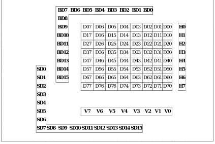
The parity encoder logic is the basic concept of the proposed design scheme. In a parity encoder a fixed length of input or a pre-calculated number of bits are taken as the input data. One redundant bit is added in the initial data and the logic value of the redundant bit depends on the type of parity encoding. For example, in even-bit parity encoding, if the number of logic-1 bits in a data sequence of length 8-bits is an odd number then the redundant bit is assigned a logic-1 value. Whereas, if the number of logic-1 bits in a data sequence of length 8-bits is an even number then the redundant bit is assigned a logic-0 value. In the 4-D parity scheme the data sequence is arranged in a matrix architecture. The encoded parity bit is generated in these four directions: horizontal, vertical, forward diagonal (slash diagonal) and backward diagonal (back slash diagonal). In the present work, the data set of 64-bits is first arranged in a matrix of size 8X8. This is shown in Fig-1. The H-V-D Parity bits are shown in Table-I. The presented scheme has 8-bits of parity in horizontal direction, 8-bits of parity in vertical direction, 15-bits of parity in slash diagonal direction and 15-bits of parity in back-slash diagonal direction. For a matrix of size “m x n”, a total of bits that are generated in the four directions is (m) + (n) + (m+n-1) + (m+n-1) = 2 ( 2 (m+n) – 1).
BD7 BD6 BD5 BD4 BD3 BD2 BD1 BD0
BD8
BD9 D07 D06 D05 D04 D03 D02 D01 D00 H0
BD10 D17 D16 D15 D14 D13 D12 D11 D10 H1
BD11 D27 D26 D25 D24 D23 D22 D21 D20 H2
BD12 D37 D36 D35 D34 D33 D32 D31 D30 H3
BD13 D47 D46 D45 D44 D43 D42 D41 D40 H4
SD0 BD14 D57 D56 D55 D54 D53 D52 D51 D50 H5
SD1 BD15 D67 D66 D65 D64 D63 D62 D61 D60 H6
SD2 D77 D76 D76 D74 D73 D72 D71 D70 H7
SD3
SD4
SD5 V7 V6 V5 V4 V3 V2 V1 V0
SD6
SD7 SD8 SD9 SD10 SD11 SD12 SD13 SD14 SD15
[image:3.612.95.518.324.608.2]
Technology (IJRASET)
TABLE ILIST OF OUTPUT PARITY BITS IN PROPOSED HVD ENCODER
HVD Parity Bits in the proposed Encoder
Horizontal Parity Bits H0, H1, H2, H3, H4, H5, H6, H7
Vertical Parity Bits V0, V1, V2, V3, V4, V5, V6, V7
Slash Diagonal Parity Bits
SD0, SD1, SD2, SD3, SD4, SD5, SD6, SD7, SD8, SD9, SD10, SD11, SD12, SD13, SD14, SD15
Back Diagonal Parity Bits
BD0, BD1, BD2, BD3, BD4, BD5, BD6, BD7, BD8, BD9, BD10, BD11, BD12, BD13, BD14, BD15
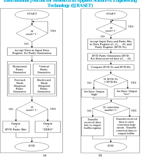
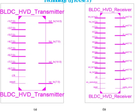
The proposed encoder is a clock synchronous hardware with a master reset input. The encoder operates to generate the 4-dimensional parity data on a logic low reset control input. If the reset input is logic high then the encoder sets all the internal registers and the output of the encoder to logic low value. The encoder involves four parallel hardware blocks to generate the parity bits. Each parity generator block is dedicated to generate particular directional parity bits. The Horizontal Parity Generator block generates horizontal parity bits “hp_tx”. The Vertical Parity Generator block generates vertical parity bits “hp_tx”. The Forward Slash Diagonal Parity Generator block generates slash diagonal parity bits “sd_tx”. The Backward Slash Diagonal Parity Generator block generates backward-slash diagonal parity bits “bd_tx”. The operational flow chart of the proposed encoder is shown in Fig-2(a).
(a) (b)
Figure 2: Operational Flow Chart (a) Proposed Encoder (b) Proposed Decoder
IV. EXPERIMENTALRESULTS
Technology (IJRASET)
[image:6.612.91.526.62.420.2](a) (b)
Fig. 3 Schematic Block Diagram (a) Proposed Encoder (b) Proposed Decoder
The hardware synthesis of the proposed design is performed using Xilinx Synthesis Tool on Xilinx FPGA Device XC3S500E-4FG320. The hardware utilization summary of the Encoder and Decoder designs are presented in Table-II.
TABLE III
HARDWARE UTILIZATION OF PROPOSED ENCODER AND DECODER
Hardwar e Resource
Total
Encoder Decoder
Use
d % Used %
Slices 4656 47 1 227 4
Flipflops 9312 68 1 184 1
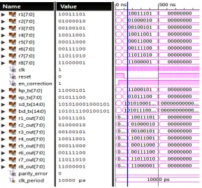
The simulation input and output of the proposed HVD Encoder are presented in Table-III. The data inputs of the proposed Decoder simulation for different conditions are given in Table-IV. The error bits are highlighted in the table. The test-bench based simulation result proposed encoder is shown in Fig-4. The test-bench based simulation result of proposed decoder for the three cases, with reference to Table-3, are shown in Fig-5, Fig-6(a) and Fig-6(b).
TABLE IIIII
SIMULATION INPUTS AND OUTPUTS OF PROPOSED ENCODER
Direction Data Symbol
Abbreviation Data Value (Binary) Data Input r1 r2 r3 r4 r5 r6 r7 r8 10011101 01000010 00100101 10011001 00011000 00111100 11011010 11000001 Parity Output hp_tx vp_tx sd_tx bd_tx 11000101 01011100 101010001000101 101011100100101 TABLE IVV
SIMULATION INPUTS OF PROPOSED DECODER
Decoder Input Case-I (without error) Case-II (with error) Case-III (with error) r1 r2 r3 r4 r5 r6 r7 r8 10011101 01000010 00100101 10011001 00011000 00111100 11011010 11000001
11111111
01000010 00100101 10011001 00011000 00111100 11011010 11000001 10011101 01000010 00100101 10011001 00011000 00111100
11111010
Technology (IJRASET)
Fig. 4 Waveform Simulation Output of proposed Decoder
[image:8.612.164.453.287.555.2](a) (b)
Fig. 6 Waveform Simulation Output of proposed Decoder with error detection and correction: (a) CASE-II (b) CASE-III
V. CONCLUSIONS
In this paper a method is proposed for error correction and detection. The scheme detects and corrects all 2-bit errors and few cases of 3-bit and 4-bit errors. The proposed implementation also generates an output signal with an error indicator. This output enables the interface circuit to take a decision regarding the acceptance or rejection of the received data. In the future this algorithm can be improved to correct all the cases of errors with 3-bits and 4-bits.
VI. ACKNOWLEDGMENT
The author wish to thank Mr. Shailesh Raghuwanshi (Principal, KNPCST, RGTU, Bhopal) and Mr. Piyush Jain (Innovative Technology Design and Training Center, Bhopal) for sharing their views in line with the present work.
REFERENCES
[1] www.xilinx.com.
[2] Vijay Tawar and Rajani Gupta, “FPGA Implementation of 4D-Parity based Data Coding Technique”, IJRET, March 2015.
[3] E. Yaakobi and T. Etzion, “High dimensional error-correcting codes”, IEEE International Symposium on proceedings in Information Theory, 2010. [4] M. Rubinoff, “N-dimensional codes for detecting and correcting multiple errors”, Communications of the ACM, Volume-4, Number-12, pp. 545-551,
1961.
[5] T. F. Wong and J.M. Shea, “Multi-dimensional parity check codes for bursty channels”, IEEE International Symposium on proceedings in Information Theory, 2001.
[6] Fernanda Lima, Luigi Carro, Ricardo Reis, “Designing Fault Tolerant Systems into SRAM-based FPGAs”, DAC Anaheim, California, June 2-6, 2003. [7] C. Argyrides, H. R. Zarndi, D K Pradhan, “Multiple upsets tolerance in SRAM Memory”, International Symposium on Circuits and Systems, New
Orleans, 2007.
[8] Y. Bentoutou, “Program Memories Error Detection and Correction On-board Earth Observation Satellites”, World Academy of Science, Engineering and Technology, 2010.
Technology (IJRASET)
Symposium, 2009.[11] S. Sharma and P. Vijayakumar, “”, International conference on Proceedings in Devices, Circuits and Systems (ICDCS), 2012.
[12] N.B. Anne, U. Thirunavukkarasu, and S. Latifi, “”, International Conference on Proceedings in Information Technology: Coding and Computing (ITCC), 2004.
[13] Guiqiang Dong, Ningde Xie and Tong Zhang, “Enabling NAND Flash Memory use Soft-Decision Error Correction Codes at Minimal Read Latency Overhead”, IEEE Transactions on Circuits and Systems, Vol. 60, September 2013.
[14] Mostafa Kishani, Hamid R. Zarandi, Hossein Pedram, Alireza Tajary, Mohsen Raji and Behnam Ghavami, “HVD: Horizontal-Vertical-Diagonal Error Detecting and correcting code to protect against soft errors”, April 2011.
[15] Costas A Argyrides, Pedro Reviriego, Dhiraj K Pradhan and Juan Antonio Maestro, “Matrix-based Codes for Adjacent Error Correction”, IEEE Transaction on Nuclear Science, Vol. 4, August 2010.