NOR AZRINNA BINTI MUHAMAD
A project report submitted in partial fulfilment of the requirement for the award of the
Degree of Master of Electrical Engineering
Faculty of Electrical & Electronic Engineering Universiti Tun Hussein Onn Malaysia
This project presents a zero-current switching (ZCS) DC-DC buck converter design, simulation and application. The converter control uses with ZCS technique to decrease the switching losses. Comparing to conventional buck converter, resonant buck converter includes a resonant tank equipped with resonant inductor and capacitor. Complete design-oriented mathematical calculations were done for ZCS converter. The converter is simulated in OrCAD Capture CIS software with design parameters. The simulation result show that the switching losses using ZCS technique is less compared to conventional buck converter.
Projek ini mempersembahkan rekabentuk pensuisan arus-sifar penukar buck DC-DC, simulasi dan aplikasi. Penukar tersebut dikawal dengan menggunakan teknik pensuisan arus-sifar untuk mengurangkan kehilangan kuasa semasa pensuisan. Jika dibandingkan dengan penukar buck konvensional, penukar resonan buck terdiri daripada resonan inductor dan resonan capacitor. Rekabentuk penuh berasaskan perkiraan matematik telah dijalankan bagi penukar buck. Penukar ini disimulasi dengan menggunakan perisian OrCAD Capture CIS. Keputusan simulasi menunjukkan kehilangan kuasa pensuisan menggunakan teknik pensuisan arus-sifar lebih rendah berbanding dengan penukar buck konvensional.
CONTENTS
TITLE i
DECLARATION ii
DEDICATION iii
ACKNOWLEDGEMENT iv
ABSTRACT v
ABSTRAK vi
CONTENTS vii
LIST OF TABLES ix
LIST OF FIGURES x
LIST OF SYMBOLS & ABBREVIATIONS xiii
LIST OF APPENDICES xv
CHAPTER 1 INTRODUCTION 1.1 Overview 1
1.2 Problem Statement 2
1.3 Objectives 2
1.4 Scope of Project 3
1.5 Layout of Project Report 3
CHAPTER 2 LITERATURE REVIEW 2.1 Introduction 4
2.2 Literature Review 5 2.3 DC-DC Converter 9 2.4 Power Semiconductor in Switching Devices 11 2.5 MOSFET Losses 13 2.6 Hard-Switching Topologies 14
2.8 Quasi-resonant Zero Current Switching Converters 18
CHAPTER 3 METHODOLOGY
3.1 Introduction 23
3.2 The Proposed Converter 23
3.3 Converter Features 24
3.4 Design Parameters 25
3.5 Mathematical Analysis of Modes of Operation 27
CHAPTER 4 SIMULATION RESULTS AND ANALYSIS
4.1 Introduction 30
4.2 Simulation of ZCS Resonant Buck Converter 30
4.3 Simulation of Buck Converter 36
4.4 Conclusion 39
CHAPTER 5 CONCLUSION & FUTURE WORKS
5.1 Conclusion 40
5.2 Suggestion for Future Work 41
REFERENCES 42
LIST OF TABLES
TABLE NUMBER TITLE PAGE
2.1 Switching Characteristics of Power Semiconductors 12
3.1 Converter Features 24
3.2 Circuit Parameters 26
LIST OF FIGURES
FIGURE NUMBER TITLE PAGE
2.1 Proposed Converter in [12] 5
2.2 Proposed Converter in [13] 6
2.3 Proposed Converter in [14] 6
2.4 Proposed Converter in [15] 7
2.5 Proposed Converter in [16] 7
2.6 Proposed Converter in [17] 8
2.7 Proposed Converter in [1] 8 2.8 Buck Converter 9 2.9 Buck converter waveforms 10
2.10 Diagram of power MOSFET 12
2.11 Equivalent MOSFET representation 14
2.12 Loss of power during hard-switching 15
2.13 Loss of power during soft-switching 16
2.14 Switch configuration for ZCS resonant converters 17
2.15 Switch configuration for ZVS resonant converters 18
2.16 Quasi-resonant half-wave ZCS buck converter 20
2.17 Quasi-resonant half-wave ZCS buck converter waveforms 20
2.18 Quasi-resonant full-wave ZCS buck converter 21
2.19 Quasi-resonant full-wave ZCS buck converter waveforms 22
3.2 Equivalent Circuit 25
4.1 The configuration of ZCS buck converter circuit 31
4.2 Resonant tank waveforms and corresponding control signal 32
4.4 MOSFET voltage and MOSFET current 33
4.5 Switch power loss of ZCS DC-DC buck converter 33
4.6 Output voltage of ZCS DC-DC buck converter 34
4.7 Output current of ZCS DC-DC buck converter 34
4.8 MOSFET voltage and MOSFET current at various switching frequencies 35
4.9 Switching power lossat various switching frequencies 36
4.10 The configuration of buck converter circuit 37
4.30 Inductor current of conventional buck converter 37
4.31 Capacitor current of conventional buck converter 37
4.32 Switch power loss of conventional buck converter 38
4.33 Output voltage of conventional buck converter 38
LIST OF SYMBOLS AND ABBREVIATIONS
SYMBOL DESCRIPTION
DC Direct Current
AC Alternating Current PWM Pulse Width Modulation BJT Bipolar Junctions Transistor IGBT Insulated Gate Bipolar Junction
MOSFET Metal Oxide Semiconductor Field-Effect Transistor ZCS Zero Current switching
ZVS Zero Voltage Switching
QR Quasi-Resonant
QRC Quasi-Resonant Circuit CCM Continuous Conduction Mode DCM Discontinuous Conduction Mode LC Inductor Capacitor
s
V Input Voltage
r
L Resonant Inductor
r
C Resonant Capacitor
s
f Switching Frequency
o
o
V Output Voltage
o
I Output Current
e
L Output Ripple Inductor / Filter Inductor
f
LIST OF APPENDICES
APPENDIX TITLE PAGE
A IRF 150 N-Channel Power Mosfet Datasheet 49
CHAPTER 1
INTRODUCTION
1.1 Overview
Advanced in power electronics in the last few decades led not only to improvements in power devices, but also to new concepts in converter topologies and controls. The various converters for different requirements are developed and related technology is studied by scientist to accomplish the research of new converters.
This work focuses on the issues related with the designing of Zero Current Switching (ZCS) buck converter. The work will append ZCS techniques, LC resonant circuits and buck topology. There is major requirement for changing the voltage from one level to another. Buck converters are one of the most important components of the circuit which operates the voltage from the desired level to fixed level.
1.2 Problem Statement
A buck converter is one of the most important and widely DC-DC converters of modern applications. The buck converters using hard switching technique generate higher switching losses and hence the efficiency becomes low. In order to improve the energy efficiency soft-switching techniques have been proposed to reduce the switching power losses across the power devices. By this reason a buck converter with soft switching technique is develop to increase the efficiency of converter.
1.3 Objectives
The designing of ZCS buck converter for USB power adapter application is the aims of this project. To achieve these aims, the objectives of this report are formulated as follow:
i. To propose soft switching buck converter with ZCS for its switch using as simple circuit as possible.
ii. To compute the optimal values of resonant converter by applying the characteristic curve and mathematical calculation from the circuit configuration.
iii. To simulate the ZCS resonant buck converter using OrCAD Capture CIS software.
iv. To analyse the resonant current and voltage waveforms and the switching voltage and current waveforms.
Scope of Project
The scopes of work for this project are:
i. Design ZCS resonant buck converter for 5V, 1.5A USB power adapter
ii. Simulation work using OrCAD Capture CIS as platform
iii. Verification of this resonant converter includes switching power losses, resonant current and voltage waveforms and output current and voltage waveforms
1.4 Layout of Project Report
This section outlines the overall structure of the report and provides a brief explanation for each chapter. This project report contained five chapters.
Chapter 2 describes the losses in switching semiconductor switch which are conduction losses and switching losses. Hard-switching is also known as switching losses. The soft-switching converter, its concept and types which includes zero voltage switching (ZVS) and zero current switching (ZCS) devices are explained. This chapter also discussed hard switching converter topology which is buck converter.
Chapter 3 presents the analysis of ZCS buck converter and its schematic diagram. The theoretical waveforms and mode of operation is discussed in detail.
Chapter 4 discusses the simulation results. The ZCS resonant buck converter is evaluated by simulation study using OrCad Capture CIS. For the comparison purpose, the simulation study of buck converter is also presented.
CHAPTER 2
LITERATURE REVIEW
2.1 Introduction
Power electronics converters are implemented with switching devices that turn on and off while power is being converted from one form to another. The power electronic converters fall generally into six categories:
i. Diode rectifier
It converts AC input voltage to a fixed DC output voltage. The input voltage to rectifier could be either single phase or three phases.
ii. AC to DC Converter (Controlled rectifier)
It converts fixed AC input voltage to a variable DC output voltage. The converter may be fed from single phase or three phases.
iii. AC to AC Converter (AC voltage regulator)
It converts a fixed AC input voltage to variable AC output voltage.
iv. DC to DC Converter (DC chopper)
v. DC to AC Converter (Inverter)
It converts a fixed DC input voltage to a fixed AC output voltage.
vi. Static switches
There are called as AC static switches or a DC static switch depends on the supply to these switches either AC or DC supply.
Power converters typically consist of semiconductor devices such as transistors and diodes, energy storage elements such as inductors and capacitors, and some sort of controller to regulate the output voltage. Transistor type devices like BJTs (Bipolar Junctions Transistors), MOSFET (Metal Oxide Silicone Field Effect Transistors) and IGBTs (Insulated Gate Bipolar Transistors) are used as switches in power electronic converters. These devices can be operated in higher switching frequencies which help to reduce converter size.
2.2 Literature Review
[image:16.595.160.479.611.729.2](Yuang-Shung Lee and Guo-Tian Chen, 2004) presented quasi-resonant converter to achieve the ZCS for reducing the loss of bi-directional converters as shown in Figure 2.1. The results indicate that the switching loss, switching waveform and EMI emission is reduced in the battery charging system with a battery equalizer. The most disadvantage of this topology is the power MOSFETs of the quasi-resonant ZCS converter have not been exactly turned on at the zero current states.
(Jaroslav Dudrik and Juraj Oetter, 2007) discussed soft switching PWM DC-DC Converters using power MOSFETs and IGBTs in reduction of switching and conduction losses. The circuit configuration of this design is shown in Figure 2.2. An important advantage of the circuit is that the rectifier diodes do not suffer from reverse recovery problem since they commutate with ZCS. The limitation of this topology is soft-switching easy to achieve at light load only.
Figure 2.2: Proposed converter in [13]
[image:17.595.126.510.596.748.2](Mohammad Mahdavi, Amin Emrani and Hosein Farzanehfard, 2010) proposed a new ZCS resonant buck converter as a soft-switching DC-DC converter using only an auxiliary switch. The circuit configuration of proposed converter is shown in Figure 2.3. The proposed converter both switches are turned on or off under ZCS condition. The most disadvantage of the topology is limitation only suitable for employing IGBT for high power.
(P.Preethi and R.Mahalakashmi, 2011) presented a concept which combines the resonant converters and switched-capacitor converters to reduce switching losses. A switched capacitor is used for resonant inverting wherein negative voltage is required. The main disadvantages of the topology is required a large number components which are two switches, some diodes and a number of switching capacitor cells as shown in Figure 2.4.
Figure 2.4: Proposed converter in [15]
(Parul Pradhan, 2012) proposed a buck converter topology with resonant configuration as shown in Figure 2.5. ZCS topology is used to diminish the switching losses in enhanced efficiency of converter. This topology is successfully done to minimize switching losses across the device, lower the current and voltage stresses formed across it and diminish the overall size of device with enhanced efficiency for use in high frequency circuits. The problem of this topology is effect of parasitic capacitance in a MOSFET that can instigate conduction without any pulse applied to its gate.
[image:18.595.128.514.588.742.2](José F. da Rocha, Marcelino Bicho dos Santos and José Manuel F.Dores Costa, 2013) presented a QR-ZCS topology to overcome voltage spikes during the switches commutation in a buck converter. The circuit configuration of this converter is shown in Figure 2.6. Results show that resonant DC-DC converters generate voltage spikes which magnitude are sometimes higher than that generated in a hard switching converter and are superimposed to the overvoltage occurring in the resonant phase. The voltage spikes generated in DC-DC converters can cause circuit malfunctions or device breakdown hence gives low energy efficiency. Therefore, this topology is not considered for this project.
Figure 2.6: Proposed converter in [17]
(G. Yanik and E.Isen, 2013) proposed a 60W full wave quasi-resonant zero-current switching buck converter to decrease the switching losses. The result states that the switching loss is zero. Therefore this topology is considered for this project. The circuit configuration of this proposed converter is shown in Figure 2.7.
[image:19.595.141.499.562.708.2]2.3 DC-DC Converter
DC-DC converter converts a fixed DC input voltage to variable DC output voltage or vice versa by varying of duty cycle. There are many types of DC-DC converter such as buck converter, boost converter, buck-boost converter and cuk converter. This project focused on buck converter.
2.3.1 Buck Converters
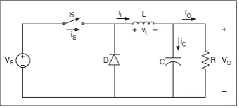
A buck converter is a step-down DC to DC converter that uses a switching device, a diode, an inductor and a capacitor as shown in Figure 2.8. Typical waveforms are shown in Figure 2.2 under assumption that the inductor current is always positive. The state of the converter in which the inductor current is never zero for any period of time is called the continuous conduction mode (CCM). It can be seen from the circuit that when switch S is commanded to the on state, the diode D is reverse biased. When the switch S is off, the diode conducts to support an uninterrupted current in the inductor.
[image:20.595.198.441.639.749.2]The DC-DC converters can operate in two distinct modes with respect to the inductor current, iL. Figure 2.9 depicts the CCM in which the inductor currents always greater than zero. When the average value of the input current is low (high R) and/or the switching frequency fs is low, the converter may enter the discontinuous conduction mode (DCM). In the DCM, the inductor current is zero during a portion of the switching period.
Figure 2.9: Buck converter waveforms
The key parameters that involved in buck converter design are discussed as follows.
The output voltage Vo is expressed as
o s
V DV (2.1) where D is the duty cycle.
The minimum value of inductance Lmin required for continuous current is
min
(1 ) 2
D R L
f
(2.2)
The value of filter inductance L for continuous-current as
1
o s o L L V D V V L D
i f i f
(2.3) where iL is the peak-to-peak ripple current in the inductor
The minimum value of capacitance Cmin required for continuous current is
min 2 1 16 D C Lf
(2.4)
The value of filter capacitance C for continuous-current as
2 1 8 o o D C V L f V (2.5)
where Vo is the peak-to-peak ripple voltage at the output
2.4 Power Semiconductor Switching Devices
When semiconductor is used as switch it is possible to control large amounts of load power with relatively low power dissipation. In an ideal case, there will be no power dissipation in the switching device. In a DC-DC converter, an input voltage and the average output voltage is controlled by controlling the switch on and off durations. Normally BJTs, MOSFETs and IGBTs are used as switching devices in DC-DC converters.
MOSFETs are used in low power applications (typically a few kilowatts) and have lower current and voltage ratings (typically a few hundreds of volts) but higher frequency well in a range of hundreds of kHz. IGBTs are used in in medium- power applications such as DC and ac motor drives, power supplies, solid-state relays and contactors. They have high voltage and current ratings, but operate in lower frequencies (up to 20kHz).
[image:23.595.144.480.311.605.2]The summary of this switching characteristics are shown in Table 2.1. Here we are opting for MOSFET because its capability in handling very high frequencies and low switching loss. Diagrams of an N-channel MOSFET are shown in Figure 2.10.
Table 2.1: Switching Characteristics of Power Semiconductors Device Power Capability Switching Speed
BJT Medium Medium
MOSFET Low Very High
IGBT Medium Medium
2.5 MOSFET Losses
The semiconductor switches used in power converters are not ideal and are a source of energy losses. The main losses that are related with these switches are conduction losses and switches losses. The magnitude of conduction and switching losses are all dependent on the application and device technology used, but even the smallest loss is undesirable as it reduces the efficiency of the system.
2.5.1 Conduction Losses
The conduction losses in MOSFETS are due its behaving as a resistor when it is in the ON state where the resistance is equal to RDS(ON), the resistance between drain and source. So the power dissipation is equal to ID2RDS ON( ). The on-state resistance is an important data sheet parameter, since it determines the forward voltage drop across the device and its total power losses.
2.5.2 Switching Losses
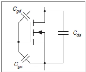
In MOSFETs, the main switching losses are caused by the charging and discharging of the gate-to-source and gate-to-drain parasitic capacitance to turn on and off the device respectively. Figure 2.11 shows the physical representation of these capacitors. The MOSFET parasitic capacitance are given in terms of the device data sheet parameters Ciss , Coss and Crss as follows.
gd rss
C C
gs iss rss
C C C
ds oss rss
where Crss= small-signal reverse transfer capacitance
iss
C = small-signal input capacitance with the drain and source terminals are shorted
oss
[image:25.595.235.400.206.344.2]C = small-signal output capacitance with the gate and source terminals are shorted
Figure 2.11: Equivalent MOSFET representation including junction capacitances
2.6 Hard-Switching Topologies
In a real semiconductor switch, the switch voltage or switch current do not go to zero instantaneously at the instant of turn-on or turn-off. There is duration of time during any switching transition (either switch turn-on or turn-off) when there is both voltage across and current through the switch. The corresponding power loss during each switching instant is the overlapped area of the switch current and voltage waveform at the instant of turn-on or turn-off of the switch. As the switching frequency increases, these transitions occur more often and the average power loss in device increases. Turning on and turning off the power electronic switches with switching losses is known as “hard switching”.
Figure 2.12 Loss of power during hard-switching
2.7 Soft-Switching Topologies
Soft switching techniques force the voltage or current to be zero during the time of transition; therefore there is no overlap between voltage and current and (ideally) no switching loss. Hence, the problem of switching losses and EMI due to hard switching converter operation is overcome by using soft switching. Size and weight of the device is reduced as the heat sink not required. There are two types of soft switching which are zero-voltage switching (ZVS) and zero-current switching (ZCS). There are many ZVS and ZCS techniques have been published. The selection of switching technique is important when dealing with high power converter.
Figure 2.13: Loss of power during soft-switching
2.7.1 Zero Current Switching Resonant Converters
In a zero current resonant, an inductor Lr is connected in series with a power switch
current waveform during the conduction time in order to create a zero-current condition for the switch to turn off.
(a) Half-wave types
[image:28.595.114.527.135.217.2](b) Full-wave types
Figure 2.14: Switch configuration for ZCS resonant converters
2.7.2 Zero Voltage Switching Resonant Converters
(a) Half-wave types
[image:29.595.198.439.76.261.2](b) Full-wave types
Figure 2.15: Switch configuration for ZVS resonant converters
2.8 Quasi-resonant Zero Current Switching Converters
2.8.1 Quasi-Resonant Half-wave Zero-current Switching
A ZCS-QRS designed for half-wave operation is shown with a buck type DC-DC converter. The schematic is shown in Figure 2.16. It is formed by replacing the power switch in conventional PWM buck converter with the zero-current resonant switch in Figure 2.14a. The circuit waveforms in steady state are shown in Figure 2.17a. The output filter inductor Lf is sufficiently large so that its current is approximately constant. Prior to the tuning the switch on, the output current Io
freewheels through the output diode Df. The resonant capacitor voltage Vcr equals to zero. At t0 the switch is turned on with ZCS. A quasi-sinusoidal current Is flows through Lr and Cr , the output filter and the load. S is then softly commutated at t1
with ZCS again. During and after gate pulse, the resonant capacitor voltage Vcr rises and then decays at a rate depending on the output current. Output voltage regulation is achieved by controlling the switching frequency. Operation and characteristics of the converter depend mainly on the design of the resonant circuit.
It can be seen from the waveform if i o
r
V I
Z
, Is will not come back to zero naturally and the switch will have to forced off, thus resulting in turn-off losses. The following parameters are defined: voltage conversion ratio M , characteristic impedance Zr, resonant frequency fr, normalized load resistance r , normalized switching frequency .
o in
V M
V
(2.5)
r r r L Z C
(2.6)
1 2 r r r f L C
L r
R r
Z
(2.8)
s r
f f
(2.9)
[image:31.595.146.490.470.731.2]The relationship between M and are shown in Figure 2.17b. It can be seen that M is sensitive to the load variation. At light load conditions, the unused energy is stored in Cr leading to an increase in the output voltage. Thus, the switching frequency has to be controlled, in order to regulate the output voltage.
Figure 2.16: Quasi-resonant half-wave ZCS buck converter
(b)
Figure 2.17: Quasi-resonant half-wave ZCS buck converter: (a) circuit waveforms; (b) relationship between M and
2.8.1 Quasi-Resonant Full-wave Zero-current Switching
If anti-parallel diode is connected across the switch, the converter will be operating in full-wave mode. The circuit schematic is shown in Figure 2.18. The circuit waveforms in steady state are shown in Figure 2.19a. The operation is similar to the one in half-wave mode. However, the inductor current is allowed to reverse through the anti-parallel diode and the duration for the resonant stage is lengthened. This permits excess energy in the resonant circuit at light loads to be transferred back to the voltage source, Vi . This significantly reduces the dependence of Vo on the output load. The relationships between M and at different r are shown in Figure 2.19b. It can be seen that M is insensitive to load variation.
[image:32.595.151.487.654.746.2](a)
[image:33.595.157.483.69.571.2](b)
CHAPTER 3
METHODOLOGY
3.1 Introduction
In ZCS, it is the current transient which forced to zero before the power device is switched. Under this state, the switch is able to turn off without current flowing through it. Therefore, the current and voltage overlap is overcome by ensuring that the switch current is zero before the voltage rises which leads to the power losses. This method is particularly useful in circuit that utilise bipolar as the main switch. However, ZCS use is not limited to bipolar device as all semiconductor switch technologies can give benefit from the transient; resulting in significantly reduced switching losses.
Typically, to induce zero current transient an inductor is allowed to resonate with a capacitor to create sinusoidal currents. The switching device is turned off when the current grows to zero-point transition.
3.2 The Proposed Converter
through the switch. The resonant circuit consists of switch S1, inductor L and a capacitor C. The LC circuit is used to stored and transfer energy from input to output in similar manner to the resonant converter. To achieve ZCS, the inductor L is connected in series with power switch S1. C is connected across the main power diode. When switch current is zero, there is a current flowing through the internal capacitance due to finite slope of the switch voltage at turn-off. This current flow causes the power dissipation in the switch. In ZCS techniques, the turn-off losing of switching devices is almost eradicated.
Figure 3.1: ZCS Resonant Buck Converter
3.3 Converter Features
The proposed ZCS buck converter for USB power adapter 5V, 1.5 A is presented. The converter features were listed in Table 3.1.
Table 3.1: Converter Features
Input voltage 12V
Output voltage 5V
Output current 1.5A
Switching frequency 200kHz
[image:35.595.165.448.613.724.2]REFERENCES
1. G. Yanik and E. Isen, “Quasi-Resonant Full-Wave Zero-Current Switching
Busk Converter Design, Simulation and Application,” Balkan Journal of
Electrical & Computer Engineering, Vol. 1, No. 2, 2013.
2. Dariusz Czarkowski, “DC-DC Converters,” Department of Electrical and
Computer Engineering, Polytechnic University, Brooklyn, New York, USA.
3. S.Y. (Ron) Hui and Henry S.H. Chung, “Resonant and Soft-switching
Converters,” Department of Electronic Engineering, City University of Hong
Kong.
4. Issa Batarseh, “The Power MOSFET,” School of Electrical, Engineering and
Computer Science, University of Central Florida.
5. Ahmad Mousavi, “Soft-switching DC-DC Converters,” University of
Western Ontario London, PhD Thesis, 2013.
6. K.H. Liu and F.C. Lee, “Resonant Switches – A Unified Approach to
Improve Performances of Switching Converters,” in Proc. Int. Telecomm.
Energy Conf., 1984, pp. 344-351.
7. K.H. Liu, R. Oruganti, and F.C. Lee, “Resonant Switches – Topologies and
Characteristics,” in Proc. IEEE Power Electron. Spec. Conf., 1985, pp. 62-67.
8. K. D. T.Ngo, “Generalized of Resonant Switches and Quasi-Resonant
DC-DC Converters,” in Proc. IEEE Power Electron. Spec. Conf., 1986, pp.
9. F.C. Lee, “High-frequency Quasi Resonant and Multi-Resonant Converter
Technologies,” in Proc. IEEE Int. Conf. Ind. Electron., 1988, pp. 509-521.
10. Muhammad H.Rashid, “Power Electronics, Circuits, Devices and
Applications,” Third Edition, Pearson/Prentice Hall, 2004.
11. Gyana Ranjan Sahu, Bimal Prasad Behera and Rohit Dash, “Design and
Implementation of ZCS Buck Converter,” National Institute of Technology,
Rourkela, Degree Thesis, May 2010.
12. Yuang-Shung Lee and Guo-Tian Chen, “ZCS Bi-directional DC-to-DC
Converter Application in Battery Equalixation For Electrical Vehicles,” 35th
Annual IEEE Power Electronics Specialists Conference, 2004.
13. Jaroslav Dudrik and Juraj Oetter, “High-Frequency Soft-Switching DC-DC Converters for Voltage and Current DC Power Sources,” Acta Polytechnica Hungarica, Vol. 4, No. 2, 2007.
14. Mohammad Mahdavi, Amin Emrani and Hosein Farzanehfard, “A New Zero Current Switching Resonant Buck Converter,” Applied electronics (AE), International Conference, 2010.
15. P.Preethi and R.Mahalakashmi. “Implementation of Zero Current Switching
in Step-Up/Step-Down Resonant Converter,” International Journal of
Engineering Science and Technology (IJEST), Vol. 3, No. 2, 2011.
16. Parul Pradhan, “Design of Resonant Circuits Based Embedded Controller For
Power Supply of LCD TV and Monitor,” National Institute of Technology,
Rourkela, Degree Thesis, May 2012.
18. Naseem Zaidi and Aziz Ahmad, “Analysis, Design and Control of Zero
Current Switching DC to DC Buck Converter,” International Journal of
Scientific and Research Publications, Vol. 2, Issue 7, July 2012.
19. Irfan Jamil, Zhao Jinquan and Rehan Jamil, “Analysis, Design and
Implementation of Zero-Current Switching Resonant Converter DC-DC
Buck Converter,” International Journal of Electrical and Electronics
Engineering (IJEEE), Vol. 2, Issue 2, May 2013.
20. S. Abinaya, A. Sivaranjani and S. Suja, “Methods of Battery Charging with
Buck Converter Using Soft-switching Techniques,” Bonfring International
Journal of Power Systems and Integrated Circuits, Vol. 1, Special Issue,
December 2011.
21. Yu-Lung Ke, Ying-Chun Chuang and Shao-Wei Huang, “Application of
Buck Zero-Current-Switching Pulse-Width-Modulated Converter in Battery
Charges,” IEEE, 2007.
22. M. Salem, A. Jusoh, N. Rumzi and N. Idris, “Implementing Buck Converter
for Battery Charger Using Soft Switching Techniques,” International Power
Engineering and Optimization Conference (PEOCO), 2013.
23. Biswajeet Panda and Ashirbad Sahoo, “Study of Soft Switching Boost
Converter Using An Auxiliary Resonant Circuit,” National Institute of
Technology, Rourkela, Degree Thesis, May 2012.
24. Daniel W. Hart, “Power Electronics,” Mc Graw Hill, 2010.
25. Muhammad H.Rashid, “Spices for Power Electronics and Electrical Power,”
![Figure 2.1: Proposed converter in [12]](https://thumb-us.123doks.com/thumbv2/123dok_us/8769607.898231/16.595.160.479.611.729/figure-proposed-converter-in.webp)
![Figure 2.3: Proposed converter in [14]](https://thumb-us.123doks.com/thumbv2/123dok_us/8769607.898231/17.595.126.510.596.748/figure-proposed-converter-in.webp)
![Figure 2.4: Proposed converter in [15]](https://thumb-us.123doks.com/thumbv2/123dok_us/8769607.898231/18.595.128.514.588.742/figure-proposed-converter-in.webp)
![Figure 2.6: Proposed converter in [17]](https://thumb-us.123doks.com/thumbv2/123dok_us/8769607.898231/19.595.141.499.562.708/figure-proposed-converter-in.webp)