N A N O R E V I E W
Open Access
Cohesive strength of nanocrystalline ZnO:Ga thin
films deposited at room temperature
Anura Priyajith Samantilleke
1*, Luís Manuel Fernandes Rebouta
1*, Vitor Garim
1, Luis Rubio-Peña
2,
Senetxu Lanceros-Mendez
1, Pedro Alpuim
1, Sandra Carvalho
1, Alexey V Kudrin
3and Yury A Danilov
3Abstract
In this study, transparent conducting nanocrystalline ZnO:Ga (GZO) films were deposited by dc magnetron sputtering at room temperature on polymers (and glass for comparison). Electrical resistivities of 8.8 × 10⁻⁴and 2.2 × 10⁻³Ωcm were obtained for films deposited on glass and polymers, respectively. The crack onset strain (COS) and the cohesive strength of the coatings were investigated by means of tensile testing. The COS is similar for different GZO coatings and occurs for nominal strains approx. 1%. The cohesive strength of coatings, which was evaluated from the initial part of the crack density evolution, was found to be between 1.3 and 1.4 GPa. For these calculations, a Young’s modulus of 112 GPa was used, evaluated by nanoindentation.
Introduction
Doped ZnO thin films are widely used as transparent electrodes in optoelectronic and electro-optic devices such as solar cells and flat panel displays [1-3], because of their unique properties, specifically low electrical resis-tivity and high transmittance in the visible spectral region [4]. These properties are obtained using substrate temperatures higher than 200°C, but growing interest in flexible substrates has led to the use of polymeric alterna-tives, which require the deposition of films at low tem-perature [5]. Furthermore, the deposition on polymeric substrates decreases the quality of the film properties [6]; therefore, the pursuit toward an understanding of the structural, electromechanical and electro-optical proper-ties of nanocrystalline (nc) thin films is crucial for device applications.
Experimental details
ZnO:Ga (GZO) thin films were deposited by dc-magne-tron sputtering on glass and polyethylene naphthalate (PEN) substrates, under an Ar atmosphere with a base pressure of 2 × 10⁻⁴Pa, from a GZO target (zinc oxide/ gallium oxide, 95.5/4.5 wt.%) of 2”diameter. A target cur-rent density of 0.6 mA/cm2was applied, and a deposition rate of 21 nm/min was obtained. No bias was applied to
the substrate holder during the depositions, which took place at room temperature. The working pressure (Pw)
was varied from 0.41 to 0.86 Pa, with the target-to-substrate distance kept at a constant 8 cm. The crystalli-nity and crystal orientation was studied using a Bruker AXS Discover D8 (Madison, USA) for X-ray diffraction (XRD). Glass substrates were used to avoid the presence of polymer substrate peaks. The electrical resistivity, car-rier concentration and Hall mobility of the coatings on glass substrates were all measured using Van der Pauw geometry under a magnetic field of 1 Tesla. The electro-mechanical tests were carried out on 10 × 40 mm2 sam-ples using a computer-controlled tensile testing machine (Minimat, Polymer Labs, Loughborough, UK), which was mounted on an optical microscope stage (Nikon Opti-phot-100, Tokyo, Japan). One of the grips of the instru-ment was displaced at a constant speed of 0.2 mm/min. The applied load and stage displacement values were recorded at 1-s intervals. Crack development was recorded through a CCD camera connected to the micro-scope, with the evolution of the crack density obtained by the subsequent video analysis. The thickness of the poly-mer substrates was measured using a Fischer Dualscope MP0R instrument (Sindelfingen, Germany).
Results and discussion Structural characterization
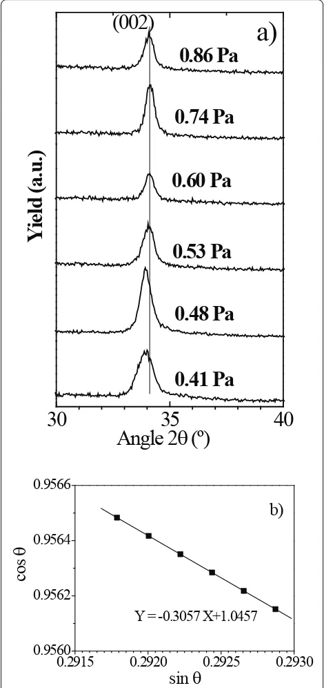
Figure 1a shows the XRD spectra obtained for nc GZO thin films (approx. 100-nm thick) as a function of the * Correspondence: anura@fisica.uminho.pt; lrebouta@fisica.uminho.pt
1
Centro de Física, Universidade do Minho, Azurém, 4800-058 Guimarães, Portugal
Full list of author information is available at the end of the article
Pw, where only the ZnO (002) peak, at approx. 34°, is
observed. The spectra reveal a highly textured hexagonal phase with a wurtzite structure. A lowerPwresulted in
samples with a higher c-lattice parameter. In the thin films prepared with aPw, between 0.41 and 0.86 Pa, the
(002) peak position shifted from 2θ= 33.93° (c = 0.528 nm) to 2θ = 34.06° (c = 0.525 nm). The full-width at half-maximum (FWHM) can be expressed as a linear
combination of the lattice strain and crystalline size. The effects of strain and particle size on the FWHM can be expressed as [7]
βcosθ/λ=1/ε+τsinθ/λ (1)
wherebis the measured FWHM,θis the Bragg angle of the peak,l is the X-ray wavelength (1.5418 Å),ε is the effective particle size and τ is the effective strain. The average particle size, calculated from the plot cosθ versus sinθshown in Figure 1b, was 8.7 nm. The parti-cle size (Dv) calculated from Scherrer’s formula (Dv=
0.94l/(bcosθ)), was 8.9 nm, which is very close to that calculated from Equation 1 [8]). The presence of strain in the ZnO crystal lattice, caused indirectly by Pw, can
be expected to exert significant influence on the mechanical properties of the nc-GZO thin film.
Optical properties
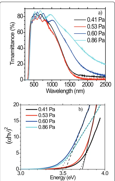
The nc nature of the thin films influences both optical and electrical performance. Figure 2 shows optical trans-mittance as a function of wavelength for thick GZO films (approx. 700 nm) prepared on glass at variousPw,
using air as a reference. The near infra-red transmit-tance is lower for Pw values of 0.41 and 0.53 Pa and
increases with higher Pw, which is consistent with the
changes observed in the electrical resistivity (discussed in the next section). The optical band gap for GZO films was calculated by plotting (ahν)2 as a function of photon energy (hν) and extrapolating the linear region of (ahν)2 to energy axis where (ahν)2 corresponds to zero. Figure 2b shows the plot of (ahν)2 as a function of photon energy (hν) for GZO films. From these plots, it can be seen that the value of the bandgap of GZO decreased from 3.73 eV (0.41 Pa) to 3.48 eV (0.86 Pa), which can be understood in the context of the Burstein Moss shift [9].
Electrical properties
The electrical resistivity, charge carrier concentration and Hall mobility as a function of thePw, for GZO films
deposited on glass, are shown in Figure 3. The resistivity of GZO samples decreased initially, and then increased with thePw. In general, the average resistivity was low
(approx. 10-4 Ωcm), which can be attributed to high carrier concentration. Considering the similarity in the conduction mechanism of electrons in GZO and ITO, the grain boundary (GB) and ionized impurity scattering processes can be considered the two dominant mechan-isms, limiting electron transport in nc-GZO films, as in the case of ITO, where other scattering mechanisms such as lattice vibrations and neutral impurity scattering may typically be neglected [10]. The relative importance of the scattering mechanism is dependent on film
30
35
40
0.41 Pa
Y
ie
ld
(a
.u
.)
Angle 2T
(º)
0.48 Pa
0.53 Pa
0.60 Pa
0.74 Pa
0.86 Pa
(002)
a)
0.2915
0.2920
0.2925
0.2930
0.9560
0.9562
0.9564
0.9566
Y = -0.3057 X+1.0457
cos
T
sin T
[image:2.595.56.291.90.588.2]b)
Figure 1XRD analysis for GZO thin films prepared under
quality and carrier concentration. Unlike intrinsic ZnO, where the conduction is generally controlled by GB-scattering, in doped ZnO at high electron density (>1020 cm-3), the ionized impurity scattering can be expected to dominate, which explains the low values of electron mobility (<10 cm2V/s) [11].
Tensile tests
Tensile tests were performed at a constant strain rate on PEN substrates (82μm) coated with GZO films (approx. 100 nm) prepared under two different Pws to increase
nominal strains. The PEN substrate is isotropic, and the elastic modulus was 4.23 GPa, as measured through the tensile test on uncoated substrate. The cracking densi-ties as a function of the substrate nominal strain for two different GZO coatings (0.53 and 0.86 Pa) are shown in Figure 4a. The crack densities at saturation of these two PEN/GZO films were 0.316 and 0.515μm-1, respectively. The coatings have similar properties and thicknesses, with small differences causing variations wholly within
acceptable margins of error. Using the weakest link model, the coating’s cohesive strength was evaluated from the early stages of the fragmentation process, assuming a Weibull-type, size-dependent probability of failure for the coating fragments of length ℓ under a stresss[12,13]:
F(σ )= 1−exp
−
0
σ β
α
(2)
Assuming that the residual stresses were negligible, in the initial stage of fragmentation, the average fragment length was related to the stress acting in the coating. The average fragment length (ℓ) is ℓ0(s/b)-a, where a
normalizing factor (ℓ0) of 1μm was chosen. In addition,
sis the axial stress acting in the coating, and aand b are the Weibull shape and scale parameters, respectively. These parameters were derived from a plot of ln(ℓ) ver-sus ln(s), shown in Figure 4b, using the initial part of the crack density evolution of the PEN/GZO coatings, displayed in Figure 4a.
The cohesive strength of the coating at critical length (ℓc) can be expressed as
σmax(c)=β
c
0
−1/α
(1 + 1/α) (3)
where Γ is the gamma function, ℓc = (3/2)ℓsat is the
critical length and ℓsat is the experimental mean
frag-ment length at saturation, which is also the inverse of the crack density at saturation [14]. As shown in Figure 4a, the GZO coatings prepared at Pwof 0.53 and 0.86
Pa revealed mean fragment lengths at saturation of 3.11 and 1.94μm, respectively.
In order to take into account its influence, the internal stress was evaluated, and the COS and the coating strength obtained with this method were corrected.
COScor= COS +εi (4)
wheresiis the internal stress andεi=si(1 - νc)/Ec, the
internal strain, withEcandνcbeing the Young’s
modu-lus and Poisson ratio, respectively, of the coating. Young’s modulus of GZO was measured by nanoinden-tation at 113 and 112 GPa from samples prepared at 0.60 and 0.86 Pa, respectively. Young’s modulus of the PEN substrate was determined from tensile testing (4.23 GPa). The cohesive strength of the coatings, which was evaluated from the initial part of the crack density evo-lution, was found to be between 1.3 and 1.4 GPa. The crack onset strains (COScor) occurs for nominal strains of 1.1 and 1.0%, respectively. The COS and cohesive strength of GZO are relatively similar to those reported in the literature for other polycrystalline conducting films [15].
500
1000 1500 2000 2500
0
20
40
60
80
0.41 Pa
0.53 Pa
0.60 Pa
0.86 Pa
T
rnam
itt
ance (
%
)
Wavelength (nm)
a)
3.0
3.5
4.0
0
5
10
15
20
0.41 Pa
0.53 Pa
0.60 Pa
0.86 Pa
(
D
h
Q
2
[image:3.595.57.291.86.456.2]Energy (eV)
b)
Summary
The material, opto-electrical properties, COS, the coat-ing cohesive strength, as well as the influence of mechanical strain on the electrical properties of nc
GZO thin films were investigated. The estimated aver-age crystalline size of nc-GZO films was approx. 8.7 nm, and the bandgap shifted from 3.73 eV (0.41 Pa) to 3.48 eV (0.86 Pa), where the low resistivity (approx. 10-4 Ω cm) and the high electron density (>1020 cm-3) explain the dominating scattering process as the ionized impurity scattering. The COS is similar for different GZO coatings and occurs for nominal strains approx. 1%. The cohesive strength of coatings, which was evaluated from the initial part of the crack density evolution, was found to be between 1.3 and 1.4 GPa, while the Young’s modulus was evaluated by nanoindentation.
Abbreviations
COS: crack onset strains; FWHM: full-width at half-maximum; GB: grain boundary; nc: nanocrystalline; PEN: polyethylene naphthalate; XRD: X-ray diffraction.
Acknowledgements
The authors acknowledge the receipt of funding from the Portuguese Foundation for Science and Technology (FCT) Grant PTDC/CTM/69316/2006, INL project 156: SIMBIO, NANO/NMed-SD/0156/2007 and the CIENCIA 2007 programme.
Author details 1
Centro de Física, Universidade do Minho, Azurém, 4800-058 Guimarães, Portugal2Engineering School, University of Cadiz, C/Chile, 1. 11002 Cádiz,
Spain3Physical-Technical Research Institute, N. I. Lobachevskiy State University, Nihzniy Novgorod, Russia
Authors’contributions
LR and SLM proposed the research work, and with APS coordinated the collaborations and carried out the analysis and interpretation of the experimental results. VG and LRP participated in sample processing, electromechanical experimental measurements, and analysis and interpretation of the results. PA, AVK and YAD carried out electrical measurements and SC performed the nanoindentation measurements. All authors read and approved the final manuscript.
Competing interests
The authors declare that they have no competing interests.
Received: 5 November 2010 Accepted: 7 April 2011 Published: 7 April 2011
References
1. Fonrodona M, Escarré J, Villar F, Soler D, Asensi JM, Bertomeu J, Andreu J:
PEN as substrate for new solar cell technologies.Sol Energy Mater Sol
Cells2005,89:37.
2. Kyaw AKK, Sun XW, Zhao JL, Wang JX, Zhao DW, Wei XF, Liu XW, Demir HV, Wu T:Top-illuminated dye-sensitized solar cells with a
room-temperature-processed ZnO photoanode on metal substrates and a Pt-coated Ga-doped ZnO counter electrode.J Appl Phys D Appl Phys2011,
44:045102.
3. Taylor MP, Readey DW, van Hest MFAM, Teplin CW, Alleman JL, Dabney MS, Gedvilas LM, Keyes BM, To B, Perkins JD, Ginley DS:The Remarkable Thermal Stability of Amorphous In-Zn-O Transparent Conductors.Adv
Funct Mater2008,18:3169.
4. Hamberg I, Granqvist CG:Evaporated Sn-doped In2O3 films: Basic optical properties and applications to energy-efficient windows.J Appl Phys
1986,60:R123.
5. Fortunato E, Gonçalves A, Assunção V, Marques A, Águas H, Pereira L, Ferreira I, Martins R:Growth of ZnO:Ga thin films at room temperature on polymeric substrates: thickness dependence.Thin Solid Films2003,
442:121.
0.4 0.5 0.6 0.7 0.8 0.9 1E-4 1E-3 1E19 1E20 1E21 0 5 10 15 20 25
resistivity Hall m
ob ility (c m 2 V -1 s -1 ) R es is tiv ity ( : .c m )
Working pressure (Pa)
carrier concentration Carri
[image:4.595.57.288.88.235.2]er co ncen tr at io n ( cm -3 ) mobility
Figure 3The electrical resistivity, carrier concentration and
Hall mobility for GZO/glass as a function of the Pw.
0
2
4
6
8 10 12 14 16 18
0.0
0.1
0.2
0.3
0.4
0.5
C
rack
d
ensi
ty
(
P
m
-1)
Nominal strain (%)
PEN/GZO (0.53 Pa)
PEN/GZO (0.86 Pa)
a)
1
10
1
10
100
1
10
1
10
100
A
ver
ag
e cr
ack sp
aci
ng
(
P
m)
Stress (GPa)
PEN/GZO (0.53 Pa)
PEN/GZO (0.86 Pa)
b)
Figure 4 Cracking density as a function of the substrate nominal strain for different GZO coatings deposited on PEN (82
[image:4.595.56.293.340.690.2]6. Lewis BG, Paine DC:Applications and Processing of Transparent Conducting Oxides.MRS Bull2000,25:22.
7. Gu F, Wang SF, Lu MK, Zhou GJ, Xu D, Yuan DR:Structure Evaluation and Highly Enhanced Luminescence of Dy3+-Doped ZnO Nanocrystals by Li + Doping via Combustion Method.Langmuir2004,20:3528.
8. Cullity BD, Stock SR:Elements of X-Ray Diffraction.3 edition. NJ: Prentice-Hall Inc; 2001, 167-171, ISBN 0-201-61091-4.
9. Park JB, Park SH, Song PK:Electrical and structural properties of In-doped ZnO films deposited by RF superimposed DC magnetron sputtering system.J Phys Chem Solids2010,71:669.
10. Robbins JJ, Harvey J, Leaf J, Fry C, Wolden CA:Transport phenomena in high performance nanocrystalline ZnO:Ga films deposited by plasma-enhanced chemical vapor deposition.Thin Solid Films2005,473:35. 11. Minami T:Transport phenomena in high performance nanocrystalline
ZnO:Ga films deposited by plasma-enhanced chemical vapor deposition.
MRS Bull2000,25:38.
12. Weibull W:A statistical distribution function of wide applicability.J Appl Mech1951,18:293.
13. Leterrier Y, Boogh L, Andersons J, Månson J-AE:Adhesion of silicon oxide layers on poly(ethylene terephthalate). I: Effect of substrate properties on coating’s fragmentation process.J Polym Sci B Polym Phys1997,
35:1449.
14. Leterrier Y:Durability of nanosized oxygen-barrier coatings on polymers.
Prog Mater Sci2003,48:1.
15. Leterrier Y, Médico L, Demarco F, Månson J-AE, Betz U, Escola MF, Olsson MK, Atamny F:Mechanical integrity of transparent conductive oxide films for flexible polymer-based displays.Thin Solid Films2004,
460:156.
doi:10.1186/1556-276X-6-309
Cite this article as:Samantillekeet al.:Cohesive strength of nanocrystalline ZnO:Ga thin films deposited at room temperature. Nanoscale Research Letters20116:309.
Submit your manuscript to a
journal and benefi t from:
7Convenient online submission
7Rigorous peer review
7Immediate publication on acceptance
7Open access: articles freely available online
7High visibility within the fi eld
7Retaining the copyright to your article