N A N O E X P R E S S
Open Access
Thermal Effects and Small Signal Modulation of
1.3-
μ
m InAs/GaAs Self-Assembled Quantum-Dot
Lasers
HX Zhao
1*, SF Yoon
1, CZ Tong
2, CY Liu
3, R Wang
1, Q Cao
1Abstract
We investigate the influence of thermal effects on the high-speed performance of 1.3-μm InAs/GaAs quantum-dot
lasers in a wide temperature range (5–50°C). Ridge waveguide devices with 1.1 mm cavity length exhibit small
sig-nal modulation bandwidths of 7.51 GHz at 5°C and 3.98 GHz at 50°C. Temperature-dependentK-factor, differential
gain, and gain compression factor are studied. While the intrinsic damping-limited modulation bandwidth is as high as 23 GHz, the actual modulation bandwidth is limited by carrier thermalization under continuous wave operation. Saturation of the resonance frequency was found to be the result of thermal reduction in the differential gain, which may originate from carrier thermalization.
Introduction
High-temperature stability in laser operation is an essen-tial characteristic required for the long-wavelength semi-conductor lasers in optical communication systems. Realization of uncooled high-speed operation of 1.3-μm quantum-dot (QD) lasers has attracted intensive research interests due to its application in optical com-munication. Over the past decade, promising dynamic properties of QDs such as large differential gain, high cut-off frequency, and small chirp were reported in devices with emission wavelength less than 1.2μm [1]. Improved temperature characteristics of QD lasers, such as temperature-invariant threshold current [1], high characteristic temperature (To) [2], and linewidth
enhancement factor [3], have been realized through
p-doping technique. However, quantum-dots emitting at 1.3 μm and above have not fulfilled the initial expecta-tion of improved temperature-insensitive modulaexpecta-tion bandwidths, which have largely remain below 12 GHz [4]. With the increase in QD size and the strain effect of the cap layer, the self-assembled (SA) InAs/GaAs QDs can emit at 1.3 μm. The energy levels are still discrete. However, the number of energy level increases and the level separation, especially for holes, becomes much
narrower (8–11 meV for hole) than that in the short-wavelength QDs. This results in significant hole therma-lization [5]. Other problems reported in the 1.3-μm SA QDs include the finite GaAs barrier and thin wetting layer [6]. These disadvantages consequently lead to the temperature-sensitive performance observed in 1.3-μm QD lasers, such as the low characteristic temperature at or above room temperature [7] and strong temperature-dependent maximum gain. Fiore et al. [8] have studied the effects of intradot relaxation on theK-factor and dif-ferential gain of quantum-dot lasers. Deppe et al. [9] have reported the role of density of states, especially thermalization of holes due to their closely spaced dis-crete energy levels. This limits the modulation speed of QDs with deep confinement potentials such as the 1.3-μm InAs/GaAs QDs. Many theoretical [8,9] and experimental [3,10,11] investigations have been per-formed to study the bandwidth limitations in long-wavelength QD lasers. According to these investigations,
K-factor [8,11] has been recognized to be one of the limiting factors for the modulation bandwidth of QD lasers, which accounts for the effect of photon lifetime, differential gain, and nonlinear gain compression factor. Despite the theoretical and experimental investigations on the effect of differential gain on the DC performance of 1.3-μm QD laser and directly modulated uncooled 1.3-μm QD laser [12], the effect of carrier thermaliza-tion on the high-speed performance of 1.3-μm QD laser * Correspondence: zhao0097@ntu.edu.sg
1
School of Electrical and Electronic Engineering, Nanyang Technological University, Singapore, 639798, Republic of Singapore.
Full list of author information is available at the end of the article
has not been analyzed systematically. Obviously, the modulation speed (or bandwidth) of the 1.3-μm QD lasers should be temperature-dependent due to the tem-perature-sensitive gain profile of QDs. As there are few investigations on the effect of temperature on the band-width of 1.3-μm QD lasers, a study on this aspect will provide greater understanding on the differential gain and carrier dynamics in long-wavelength QD lasers.
In this paper, we investigate the influence of thermal effects on the high-speed modulation characteristics of 1.3-μm InAs/GaAs QDs by studying the temperature-dependent small signal modulation behavior. The effects of temperature on the K-factor, differential gain, and nonlinear gain compression will be presented here.
Experimental Details
The ten-layer self-assembled InAs/GaAs QD laser struc-ture, as shown in Figure 1, was grown on GaAs (100) substrate by molecular beam epitaxy (MBE). The struc-ture consists of QD active region sandwiched between two 1.5-μm C- and Si-doped Al0.35Ga0.65As cladding
layers. The active layer comprises 2.3 monolayer (ML) of InAs QDs capped by a 5-nm In0.15Ga0.85As layer. A
33-nm GaAs layer is used to separate the two QD layers [13]. The wafer was processed into 4-μm-wide ridge waveguide (RWG) lasers by standard photolithography process and wet chemical etching at room temperature (RT) [14]. Ridge height of approximately 1.3 μm was obtained before the pulsed anodic oxidation (PAO) pro-cess. A 200 ± 5 nm-thick oxide layer was formed by PAO method, whose experimental setup can be found in [15]. Subsequently, p-contact layers (Ti/Au, 50/300 nm) were deposited by electron beam evaporation, while n-contact layers (Ni/Ge/Au/Ni/Au, 5/20/100/25/300
nm) were deposited on the backside of the substrate fol-lowing lapping down to ~100 μm. Finally, the wafer was cleaved into laser bars and the cleaved facets were left uncoated. The devices were mounted p-side down on a heat sink for measuring the small signal modulation characteristics. The small signal modulation response of the QD lasers was measured under continuous wave (CW) biasing condition using a vector network analyzer (VNA), a high-speed photoreceiver and laser diode cur-rent source. A thermoelectric temperature controller was used to regulate and monitor the device tempera-ture during measurements.
Results and Discussions
The measured CW Power-Current performance of a device with cavity length of 1.1 mm shows that the threshold current (Ith) and slope efficiency are 55 mA
and 0.27 W/A at room temperature, respectively. Maxi-mum output power of 96 mW occurred at injection cur-rent of 395 mA. Figure 2 shows the lasing spectrum of the laser device under injection current of 100 mA at RT for verification. The lasing wavelength is centered at 1,306.5 nm. Furthermore, no lasing at excited state was observed. Characteristic temperatureTois around 41 K
from 5 to 50°C. The small signal modulation response under different injection current levels is shown in Figure 3. At room temperature, the highest bandwidth of 6.1 GHz was obtained at injection current level of 390 mA. For injection current more than 395 mA, the resonance frequency frdecreases with increasing
injec-tion current. This is because, there are two competing factors affecting the resonance frequency: (1) increase in resonance frequency with injection current and (2) decrease in resonance frequency due to internal heating.
Metal
p-doped Al0.35Ga0.65As (1000nm) p=1 18
p-doped Al0.35Ga0.65As (500nm) p=5 17
n-doped Al0.35Ga0.65As (500nm) n=5 17
n-doped Al0.35Ga0.65As (1000nm) n=1 18
n-doped GaAs Buffer (500nm) n=3 18
p-doped GaAs (200nm) p=1 1020
p-doped Al0.35Ga0.65As (20nm) p=3 18
GaAs (33nm)
In0.15Ga0.85As (5nm)
InAs QDs GaAs Barrier (33nm)
n-doped Al0.35Ga0.65As (20nm) n=3 18
n-doped GaAs substrate Metal
[image:2.595.57.282.513.704.2]10
Figure 1The schematic diagram of the InAs/GaAs ten-layer QD laser structure.
[image:2.595.297.538.520.703.2]Therefore, when injection current increases higher than 395 mA, the internal heating resulted from the increased current becomes dominant and leads to the decrease in resonance frequency. The small signal mod-ulation response was further fitted into a transfer func-tion that accounts for the intrinsic response of the laser as well as the extrinsic effects [16]:
H f f
f f j f j f
f
( )= ⋅
− + ⋅ +
const r
r
p 2
2 2
2
1
1
(1)
where fris the resonance frequency, gis the damping
rate, andfpis the parasitic cut-off frequency. From the
fitting, we obtained values of the damping rate gand resonance frequency fr at different bias currents.
The parasitic cut-off frequency is almost temperature-independent and only restricts the bandwidth minimally. According to the plot of fr vs. the square root of the
normalized bias current (I–Ith)1/2, the slope (known as
D-factor or modulation efficiency) is obtained to be 0.28 GHz/mA1/2at RT. The relationship between resonance frequency and damping rate defines the K-factor, which is 0.83 ns at RT. Furthermore, the K-factor is directly related to the damping-limited bandwidth (f3dB,damping)
by [16]:
f
K 3
2 2
dB,damping =
(2)
The internal quantum efficiency (hi) and internal
opti-cal loss (ai) of the devices were estimated to be 51%
and 4 cm-1 by measuring lasers with different cavity length (1–3 mm) [17,18]. The internal quantum
efficiency and internal optical loss exhibit weak depen-dency on temperature. With the values of internal quan-tum efficiency and internal optical loss, the differential gain (dg/dn) and nonlinear gain compression factor (ε) are extracted. The gain derivatives with respect to the carrier population defines differential gain, while the nonlinear gain compression factor is used to describe the gain dependence on the photon density. From the value of the D-factor, the differential gain is obtained to be 11.1 × 10⁻¹⁵ cm2 at RT, which is almost ten times higher than that reported in literature [19] (differential gain of 1 × 10-15 cm2 at 300 K for a device emitting at 1,263 nm). The nonlinear gain compression factor is determined to be 12 × 10-16cm3 at RT. Note that the results are different from that reported recently [20]. We believe that the differences are due to the different device dimensions considered since the performance depends strongly on the device dimensions [21,22].
Measurements of direct small signal modulation of the QD laser were carried out from 5 to 50°C. Figure 4 shows the maximum measured (triangles) bandwidth (f3dB,measured) as function of temperature. The maximum
measured bandwidth decreases almost linearly with tem-perature as temtem-perature increases from 5 to 50°C. The highest f3dB,measuredof 7.51 GHz occurred at 5°C. The
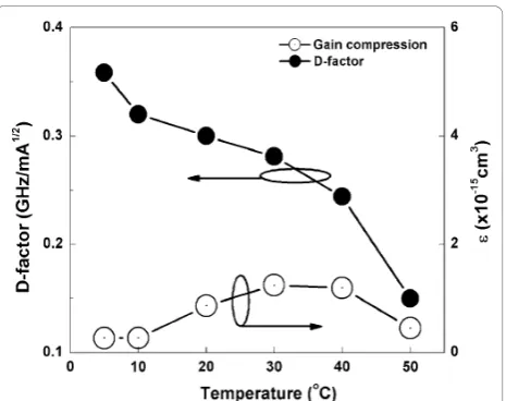
[image:3.595.58.291.88.277.2]D-factor is 0.36 GHz/mA1/2at 5°C and 0.15 GHz/mA1/2 at 50°C as shown in Figure 5 (solid circles). The differ-ential gain from 5 to 50°C decreases following increase in temperature as shown in Figure 6. Figure 7 shows the calculatedK-factor of the QD laser as function of tem-perature. There is a significant increase in theK-factor as temperature increases. The calculated K-factor increases approximately by a factor of three over the temperature range of 5–50°C.
[image:3.595.306.539.518.692.2]Figure 3Small signal modulation response measured at RT under different injection current levels.
Figure 4Calculated thermal- (squares) and damping-limited
(circles) bandwidth (BW) and plot of the measured (triangles)
From (2), thef3dB,dampingof the QD laser is 23 GHz at
5°C and 8.9 GHz at 50°C, which is limited by the carrier-capture time and modal gain via theK-factor [11,23]. This shows that the 1.3-μm InAs/GaAs QD lasers can potentially operate at very high frequencies. However, our experimental data shows much lower bandwidth. This can be attributed to the thermal effects, i.e., the thermal saturation of photon number (So) at roll-over
current injection due to the self-heating. It could also be caused by serious hole thermalization due to the closely spaced hole levels in 1.3-μm InAs QDs. Considering the dependence of bandwidth on resonance frequency, this suggests that the saturation of the bandwidth is caused by saturation of the photon density. Saturation of the photon density could possibly be caused by the strong
gain compression. Meanwhile, the nonlinear gain com-pression factor is in the order of 10-16cm3and shows a relatively weak dependence on temperature [refer to Figure 5 (hollow circle)]. Theε·Soproduct is less than
0.1, which suggests that the effect of the gain compres-sion on the resonance frequency is relatively small. At relatively small damping effects, the thermal-limited bandwidth (f3dB,thermal) is related tofrby [16]:
f3dB,thermal = 1+ 2fr,max (3)
wherefr,maxis the maximum resonance frequency at a
constant temperature. Thefr,maxof 6.6 GHz at 5°C and
2.5 GHz at 50°C would give a thermal-limited band-width of 10 GHz and 3.9 GHz (squares in Figure 4), respectively. This suggests that the main limitation on the bandwidth might be due to the decrease in differen-tial gain, which may result from the thermal effects related to carrier thermalization in the multi-stack quan-tum-dots. The origin of the temperature-dependent dif-ferential gain is currently under investigation. The incorporation of p-type modulation doping and tunnel injection might be useful to improve the QD laser per-formance by reducing the thermal effects.
Finally, the calculated intrinsic damping-limited band-width (squares) and thermal-limited bandband-width (circles) are shown in Figure 4 in comparison with the experi-mental results f3dB,measured (triangles). The
thermal-limitedf3dB,thermalis in close agreement with the
experi-mental results, indicating that the bandwidth measured in this study was limited by thermal effects.
Conclusion
[image:4.595.59.292.87.271.2]In conclusion, we have studied the influence of thermal effects on the small signal modulation characteristics of undoped InAs/GaAs QD lasers. The role of
[image:4.595.303.540.88.264.2]Figure 5 The dependence of D-factor (solid circle) and nonlinear gain compression (hollow circle) on temperature.
Figure 6The differential gain at different temperatures.
[image:4.595.58.291.518.711.2]temperature-dependent differential gain and nonlinear gain compression factor in determining the frequency bandwidth was investigated. Calculation of the tempera-ture-dependent bandwidth of the undoped QD laser shows close agreement between the thermal-limited bandwidth and the measurement results. The bandwidth of the undoped InAs/GaAs QD lasers is mainly limited by thermal effects, which may result from carrier ther-malization in the undoped QD laser structure.
Acknowledgements
The authors would also like to acknowledge the assistance of Dr. Ngo Chun Yong and Dr. Loke Wan Khai for their useful inputs to this research.
Author details
1
School of Electrical and Electronic Engineering, Nanyang Technological University, Singapore, 639798, Republic of Singapore.2Photonics Group,
Edward S. Rogers Sr. Department of Electrical and Computer Engineering, University of Toronto, 27 King’s College Circle, Toronto, ON Canada.3Institute
of Solid State Physics, Technical University of Berlin, Hardenbergstr. 36, 10623, Berlin, Germany.
Received: 2 August 2010 Accepted: 10 September 2010 Published: 26 September 2010
References
1. Fathpour S, Mi Z, Bhattacharya P:IEEE Photonics Technol Lett2005,17:2250. 2. Shchekin OB, Deppe DG:IEEE Photonics Technol Lett2002,14:1231. 3. Cong DY, Martinez A, Merghem K, Ramdane A, Provost JG, Fischer M,
Krestnikov I, Kovsh A:Appl Phys Lett2008,92:191109.
4. Kim SM, Wang Y, Keever M, Harris JS:IEEE Photonics Technol Lett2004, 16:377.
5. Shchekin OB, Deppe DG:Appl Phys Lett2002,80:2758. 6. Xu DW, Yoon SF, Tong CZ:IEEE J Quantum Electron2008,44:879. 7. Mukai K, Nakata Y, Otsubo K, Sugawara M, Yokoyama N, Ishikawa H:IEEE J
Quantum Electron2000,36:472.
8. Fiore A, Markus A:IEEE J Quantum Electron2007,43:287.
9. Deppe DG, Huang H, Shchekin OB:IEEE J Quantum Electron2002,38:1587. 10. Gyoungwon P, Shchekin OB, Deppe DG:IEEE J Quantum Electron2000,
36:1065.
11. Ishida M, Hatori N, Akiyama T, Otsubo K, Nakata Y, Ebe H, Sugawara M, Arakawa Y:Appl Phys Lett2004,85:4145.
12. Todaro MT, Salhi A, Fortunato L, Cingolani R, Passaseo A, De Vittorio M, Della Casa P, Ghiglieno F, Bianco L:IEEE Photonics Technol Lett2007,19:191. 13. Cao Q, Yoon SF, Liu CY, Ngo CY:Nanoscale Res Lett2007,2:303.
14. Wang R, Tong CZ, Yoon SF, Liu CY, Zhao HX, Cao Q:IEEE Electron Device
Lett2009,30:1311.
15. Yuan S, Jagadish C, Kim Y, Chang Y, Tan HH, Cohen RM, Petravic M, Dao LV, Gal M, Chan MCY, Li EH, O JS, Zory PS Jr:IEEE J Sel Top Quantum Electron 1998,4:629.
16. Coldren LA, Corzine SW: Wiley; 1995.
17. Kirstaedter N, Schmidt OG, Ledentsov NN, Bimberg D, Ustinov VM, Egorov AY, Zhukov AE, Maximov MV, Kopev PS, Alferov ZI:Appl Phys Lett 1996,69:1226.
18. Kim J, Chuang SL:IEEE J Quantum Electron2006,42:942.
19. Kuntz M, Ledentsov NN, Bimberg D, Kovsh AR, Ustinov VM, Zhukov AE, Shernyakov YM:Appl Phys Lett2002,81:3846.
20. Zhao HX, Yoon SF, Ngo CY, Wang R, Tong CZ, Liu CY, Cao Q:IEEE Photonics
J2010,2:630.
21. Liu CY, Qu Y, Yuan S, Yoon SF:Appl Phys Lett2004,85:4594.
22. Liu CY, Yoon SF, Fan WJ, Uddin A, Yuan S:IEEE Photonics Technol Lett2006, 18:791.
23. Klotzkin D, Bhattacharya P:IEEE J Lightwave Technol1999,17:1634.
doi:10.1007/s11671-010-9798-4
Cite this article as:Zhaoet al.:Thermal Effects and Small Signal
Modulation of 1.3-μm InAs/GaAs Self-Assembled Quantum-Dot Lasers.
Nanoscale Res Lett20116:37.
Submit your manuscript to a
journal and benefi t from:
7Convenient online submission 7Rigorous peer review
7Immediate publication on acceptance 7Open access: articles freely available online 7High visibility within the fi eld
7Retaining the copyright to your article