N A N O E X P R E S S
Open Access
Effect of In/Al ratios on structural and optical
properties of InAlN films grown on Si(100) by
RF-MOMBE
Wei-Chun Chen
1*, Yue-Han Wu
2, Chun-Yen Peng
2, Chien-Nan Hsiao
1and Li Chang
2Abstract
InxAl1-xN films were deposited on Si(100) substrate using metal-organic molecular beam epitaxy. We investigated the effect of the trimethylindium/trimethylaluminum (TMIn/TMAl) flow ratios on the structural, morphological, and optical properties of InxAl1-xN films. Surface morphologies and microstructure of the InxAl1-xN films were measured by atomic force microscopy, scanning electron microscopy, X-ray diffraction (XRD), and transmission electron microscopy (TEM), respectively. Optical properties of all films were evaluated using an ultraviolet/visible/infrared (UV/Vis/IR) reflection spectrophotometer. XRD and TEM results indicated that InxAl1-xN films were preferentially oriented in thec-axis direction. Besides, the growth rates of InxAl1-xN films were measured at around 0.6μm/h in average. Reflection spectrum shows that the optical absorption of the InxAl1-xN films redshifts with an increase in the In composition.
Keywords:InAlN; In/Al ratios; RF-MOMBE
Background
Recently, InAlN film is a highly attractive III-nitride se-miconductor with numerous potential applications be-cause InAlN has band gap energy in the range from 6.2 eV for AlN to 0.7 eV for InN. Therefore, InAlN alloys are attractive for possible applications in light-emitting diode (LEDs) and high-efficiency multijunction tandem solar cell in the wide spectral range from ultraviolet to infrared [1-3]. In addition, compared with Ga(In, Al)N, InAlN has not been so intensively investigated because the growth of InAlN suffers from the difficulty of phase separation due to large immiscibility, optimum growth temperatures, lattice constant, bonding energy, and dif-ference of thermal stability between InN and AlN [4]. Moreover, few studies have been performed because InAlN has an unstable region concerning miscibility [5]. Therefore, it was very difficult to grow high-quality InAlN since there were many variables in the growth condition.
Previous studies of InAlN growth on an AlN buffer layer show that it has improved the crystallinity of the InAlN films and prevented oxygen diffusion from the substrate [6]. Besides, the growth of the InAlN film in all composition regions has been realized with the molecu-lar beam epitaxy (MBE) growth method [7], while it was reported that In-rich InAlN with an In content >32% grown by metal-organic vapor phase epitaxy (MOVPE) showed the phase separation [8]. Also, Houchin et al. in-dicated that the film quality of InAlN was degraded with increasing Al content. However, phase separation is not observed for the films obtained in their study [9]. Kariya et al. conclude that lattice matching is important in or-der to grow high-quality InAlN with a smooth surface morphology [10]. Especially, Guo and coworkers [11] fabricated the first single-crystal AlxIn1-xN films with x
being from 0 to 0.14 in the low-Al composition regime using MOVPE. On the other hand, Sadler et al. indicated that trimethylindium flux was increased; the indium in-corporation initially increased but then leveled off; and for further increases, the amount of indium on the sur-face as droplets increases significantly [12]. Various growth techniques have been used for growth of InAlN films, such as radio-frequency molecular beam epitaxy
* Correspondence:[email protected]
1
Instrument Technology Research Center, National Applied Research Laboratories, 20 R&D Rd. VI, Hsinchu Science Park, Hsinchu 30076, Taiwan Full list of author information is available at the end of the article
(RF-MBE) [13], metal-organic chemical vapor deposition (MOCVD) [14], pulse laser deposition (PLD) [15], and magnetron sputtering [16].
On the other hand, silicon is a very promising material for growth of III-nitride materials, with its good thermal conductivity which is especially interesting for electro-nic applications [17] and also for low-cost light-emitting diode (LED) applications [18]. Also, very few studies in-dicated that In-rich InAlN films were grown on Si sub-strate using radio-frequency metal-organic molecular beam epitaxy (RF-MOMBE), although InAlN films often were grown by MOCVD and MBE methods. Compared with the MOCVD method, the RF-MOMBE technique generally has the advantage of a low growth temperature for obtaining epitaxial nitride films [19,20]. Also, our previous study indicated that the RF-MOMBE growth temperature for InN-related alloys was lower than the MOCVD growth temperature [21].
In this paper, the InAlN films were grown on Si(100) by RF-MOMBE with various trimethylindium/trime-thylaluminum (TMIn/TMAl) flow ratios. Structural pro-perties and surface morphology are characterized by high-resolution X-ray diffraction (HRXRD), transmis-sion electron microscopy (TEM), atomic force microscopy (AFM), and scanning electron microscopy (SEM). Optical properties of all InAlN films were also investigated by an ultraviolet/visible/infrared (UV/Vis/IR) reflection spectro-photometer with integrating sphere.
Methods
Highlyc-axis-oriented InAlN films were deposited on Si (100) substrate using RF-MOMBE. The RF-MOMBE growth chamber was evacuated to a base pressure of 5 × 10⁻⁹Torr by a turbomolecular pump. TMIn and TMAl without any carrier gas were used for group III precursor. The active nitrogen radicals were supplied by a radio-frequency plasma source (13.56 MHz). TMAl and TMIn precursors were kept at room temperature and 55°C, re-spectively. By changing the TMIn/TMAl flow ratio from 1.29 to 1.63 under a constant nitrogen supply with a flow
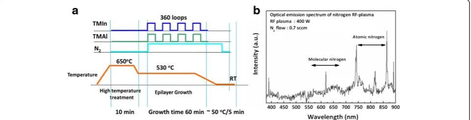
rate of 0.7 sccm and an RF plasma power of 400 W, InAlN films were grown at 530°C for 1 h to investigate the effect of the V/III ratio. The Si(100) substrates were cleaned in a wet bench using Radio Corporation of America (RCA) processes for about 30 min. Also, the substrate fol-lowed wet etch in buffered oxide etch (BOE) for 30 s, and then into the growth chamber for InAlN growth. Prior to InAlN growth, the Si substrate in base pres-sure (5 × 10⁻⁹ Torr) was heated at 650°C for 10 min for substrate surface cleaning. After, the substrate tempe-rature was decreased to 530°C for all InAlN film growth. During the deposition, the substrate temperature was monitored by a thermocouple (contact with heater back-side). The growth sequence of the unit cells of TMIn/ TMAl is described in Figure 1a. There are three unit cells; 10-s pulses of TMIn, 10-s pulse of TMAl, and normal open of atomic nitrogen were introduced alternately into the growth chamber. Figure 1b shows the optical emission spectrum of the nitrogen RF plasma with a nitrogen pres-sure of 7 × 10⁻⁶Torr in the growth chamber. It is notable that there are a number of emission peaks associated with molecular and atomic nitrogen transitions that appear in this spectrum. The dominant emission peaks at 740, 820, and 860 nm indicate that a significant amount of atomic nitrogen is produced in the N2RF plasma.
The X-ray diffraction (Siemens D5000, Siemens Co., Munich, Germany) measurements were carried out in a
[image:2.595.59.540.581.704.2]θ-2θcoupled geometry using Cu-Kαradiation to identify the presence of secondary phases or crystalline struc-tures. The lattice parameters of InxAl1-xN films and the value of xwere calculated by high-resolution X-ray dif-fraction (Bruker D8, Bruker Optik GmbH, Ettlingen, Germany). The diffraction angle 2θ was scanned from 20° to 40° at 0.005°/s. The surface and cross-sectional morphologies of the InxAl1-xN films were analyzed using a field-emission scanning electron microscope (FE-SEM, Hitachi S-4300, Hitachi, Ltd., Chiyoda, Tokyo, Japan). The microstructure of the InAlN films was investigated in detail by TEM in cross-sectional configuration (TEM, Philips Tecnai 20 (FEI/Philips Electron Optics, Eindhoven,
Figure 1Growth sequence of RF-MOMBE and spectrum of a nitrogen RF plasma. (a)Growth sequence of RF-MOMBE pulses for InAlN films.
Netherlands) and JEOL 2010 F (JEOL Ltd., Akishima, Tokyo, Japan)). The InxAl1-xN film's composition was de-termined with HRXRD. The optical reflectance measure-ments were performed by using a UV/Vis/IR reflection spectrophotometer with integrating sphere (PerkinElmer Lambda 900, PerkinElmer, Waltham, MA, USA) from 200 to 2,000 nm.
Results and discussion
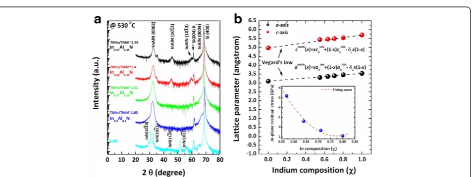
Figure 2a shows the θ-2θ scan XRD pattern for the InAlN films grown at 530°C with the TMIn/TMAl flow ratio of 1.29, 1.4, 1.51, and 1.63. The XRD pattern indica-ted that the peaks corresponding to InAlN (0002), (1011), (1012), and (1013) were observed for InAlN films grown on the Si(100) substrate. Also, the XRD results of InN and InAlN films reveal that all the films are of wurtzite struc-ture which is preferentially oriented in thec-axis direction. No metallic indium peak was detected in the XRD pattern. In addition, it is clearly observed that peaks of all InAlN shifted depending on In composition. However, the crys-talline quality of the InAlN films degrades with increasing Al content. The result is in agreement with the report of Houchin et al.[9].
Vegard's law [22] has been applied to determine the average In composition of the ternary alloy films via measurement of lattice parameters from HRXRD.
Assuming Vegard's law to hold for InxAl1-xN and
con-sidering the biaxial strain in the layer, the indium com-position can be determined by applying the relation. Therefore, the exact indium mole fractionxof the alloy, considering the deformation of the unit cell, is
x¼− ac 1þvð Þx
−acAlN
0 −aAlN0 cvð Þx acAlN
0 −acInN0 −aInN0 cvð Þx þaAlN0 cvð Þx
where ν(x) is Poisson's ratio defined as ν(x)= 2C13/C33;
C13 and C33 are the elastic constants of the hexagonal
III-nitrides. The material constants used in this study are a= 0.311 nm, c= 0.498 nm [23], C13= 99 GPa, and
C33= 389 GPa for AlN [24]; and a= 0.354 nm, c=
0.5706 nm [23], C13= 121 GPa, and C33= 182 GPa for
InN [25]. For InxAl1-xN ternary alloy, both lattice
con-stants and Poisson's ratio v(x) are obtained by linear interpolation from the values of binaries. As a result, it can be concluded that the molar fraction of InN on a biaxially strained InxAl1-xN film is the only possible
so-lution between 0 and 1 for the following third-order
equation which presents x as a function only of two
variables. The In composition (x) is accordingly to be
calculated as x= 0.57 ± 1% (TMIn/TMAl, approximately
1.29), 0.64 ± 1% (TMIn/TMAl, approximately 1.4), 0.71 ± 1% (TMIn/TMAl, approximately 1.51), and 0.80 ± 1% (TMIn/TMAl, approximately 1.63) by Vegard's law.
The XRD pattern of an In content of <0.64 exhibits extremely weak and broad peaks, which indicates that the film is of poor quality due to structural defects. Also, the In0.64Al0.36N film shows a polycrystalline structure, suggesting that the in-plane residual stress of the In0.64Al0.36N film is almost relaxed after growth.
[image:3.595.63.540.525.704.2]At above x= 0.71, the pattern indicates that the InAlN films are preferentially oriented in the c-axis direction. In addition, a weak shoulder peak (2θ, approximately 31.909°) was detected at the highest In content of ap-proximately 0.71, indicating an intermediate layer be-tween the film and the Si substrate. As can be seen in Figure 2b, the lattice parameters for c-axis and a-axis obtained from symmetric (0002) and asymmetric (1012) diffractions of InAlN increased with the increase of In content. The results agree with the theoretical calcula-tions and report of Guo et al. [26].
Figure 2b shows the calculated lattice parameters of all InxAl1-xN films with various In compositions. Bothcand
a lattice parameters exhibit essentially a linear depend-ence on the In composition with very small deviations from Vegard's law. In our results, the bowing parameters of δa= 0.0412 ± 0.0039 Å and δc=−0.060 ± 0.010 Å
de-scribe the deviations from Vegard's rule. Therefore, the variation of the InxAl1-xN lattice parameters with In con-tentxcan be approximated as follows:
cInAlNð Þ ¼x xcInN
0 þð1−xÞc0AiN−δcxð1−xÞ
aInAlNð Þ ¼x xaInN
0 þð1−xÞa0AiN−δaxð1−xÞ
where InN and AlN lattice parameters are based on a
previous study (for InN, a= 3.538 Å and c= 5.706 Å
[27]; for AlN,a= 3.11 Å andc= 4.98 Å) [23].
The lattice parameter of the In0.57Al0.43N film was calculated to be larger than the theoretical value, which may be caused by phase separation and/or lattice strain. The in-plane residual stress of all InAlN films is shown in the inset of Figure 2b. The residual stress was tensile at an In content of >71%. The compressive stresses oc-curred in the films deposited at an In content of <64%. When the In content is high (>71%), small tensile intrin-sic stresses are observed. It has been proposed that one reason for the occurrence of tensile intrinsic stresses is the existence of numerous grain boundaries. Therefore, small tensile residual stresses were obtained at an In
content of >71%, and large compressive stresses were obtained at In compositionx= 0.57.
[image:4.595.58.537.459.704.2]Figure 3a,b,c,d shows surface morphologies and cross section of InxAl1-xN films which were prepared on Si (100) with different In/Al ratios. Also, the surface rough-ness is larger than in other reports [28] due to high-density grain boundaries and island growth. Besides, the grain size of InxAl1-xN decreases with the increase of TMIn mass flow which may be due to the indium inter-stitials. Thus, both AFM and SEM measurement results show that the use of smaller TMIn mass flow leads to a reduction in the surface roughness of the InAlN film. Also, the thickness of the grown InAlN in this study was increased with increasing TMIn mass flow. Besides, growth rates of all InAlN films were around 0.35 μm/h at x= 0.57, 0.43 μm/h at x= 0.64, 0.5 μm/h at x= 0.71, and 0.6μm/h atx= 0.80, respectively. Moreover, the sur-face of In0.80Al0.2N film was clearly observed to be rough, as compared with those of the other reports of InxAl1-xN layers [16]. Figure 3e shows that the growth rate depended on the TMIn mass flow. It is clearly seen that by increasing the TMIn/TMAl flow ratios from 1.29 to 1.63, the growth rate of the films was increased from 0.35 to 0.6 μm/h. However, the increase of the surface roughness with the increase of growth rate may be due to the 3-D growth mode. The insets in Figure 3e show the AFM images corresponding to SEM images of the surface morphologies for the InAlN films.
Figure 4a shows a cross-sectional bright-field TEM image of the In0.71Al0.29N film. The image clearly shows
Figure 3SEM cross-sectional images. (a-d)Top-view and cross-sectional SEM images of InxAl1-xN films.(e)Growth rate of InAlN films with
that the structural characteristics of the In0.71Al0.29N film exhibited a rough surface and columnar structure at the cleavage. In addition, existence of no metallic In inclusions can be observed in the images which agree with the XRD results. Besides, the selected-area diffrac-tion pattern (SAD) reveals InAlN/Si reflecdiffrac-tions shown Figure 4b. Individual diffraction rings can be identified as InAlN reflections, indicating that it is a polycrystal-line InAlN film with preferredc-axis.
Figure 5a shows the high-angle annular dark-field (HAADF) cross-sectional image of the In0.71Al0.29N film
[image:5.595.58.538.90.194.2] [image:5.595.60.292.395.707.2]which is taken in the [110]Si zone axis projection. The image shows that the two layers are visible. The top layer exhibited a thickness of about 420 nm which was measured at an indium content x of approximately 0.71 by scanning transmission electron microscopy with energy-dispersive spectroscopy (STEM-EDS). The bright layer of about 80 nm was observed at bottom regions which are indium-rich. On the other hand, the STEM-EDS line scan profile shows between InAlN films to Si substrate as shown in Figure 5b. From the top layer, cross-sectional line scan profiling of the InAlN film showed that the major In and Al elements were homo-geneously distributed over the cross section of the stem. The result was observed to be similar to MOCVD growth of AlInN films on the GaN layer [29]. The aver-age concentrations in the brighter regions are roughly estimated to be 70% ± 5% In and 30% ± 5% Al, while the Figure 4TEM images of the cross section of In0.71Al0.29N/Si. (a)Cross-sectional TEM image and(b)the SAD pattern from the In0.71Al0.29N film.
Figure 5HAADF analysis of In0.71Al0.29N films. (a)HAADF
[image:5.595.306.539.455.707.2]micrograph and(b)EDS line scan of the In0.71Al0.29N film.
Figure 6Reflection spectra of InxAl1-xN films at various in
concentrations in the darker areas are 64% ± 5% In and 36% ± 5% Al.
The optical properties of InxAl1-xN films were investi-gated by measuring the optical reflectance spectra on a UV/Vis/IR spectrophotometer with integrating sphere (200 to 2,000 nm). The reflectance spectra of all InxAl1-xN films are as shown in Figure 6. Prominent Fabry-Perot interference fringes attributed to multiple-layer-substrate reflections are observed at a long wavelength. However, Fabry-Perot interference fringes increase with the increase of film thickness, since the interference fringe begins to disappear in the vicinity of the wavelength related to the optical absorption edge [30]. In addition, light scattering-induced changes may have occurred in the surface of po-lycrystalline InAlN films due to surface roughness such as grain, grain boundaries, and microscopic pores. The reflection spectra shows that the optical absorption of the InAlN films redshifts with an increase in the In composition x.
Conclusions
Highly c-axis-oriented InxAl1-xN films were grown on Si(100) by RF-MOMBE. From XRD results, In0.71Al0.29N has the best crystalline quality among the InxAl1-xN
sam-ples for various values of the In composition fraction x studied here. However, the strain of all InAlN films has not been relaxed after growth. At an In content of <57%, the InAlN/Si(100) exhibits worse crystallinity which ob-served obviously large residual stress. The surface rough-ness of InAlN films increased with the increase of In composition. The corresponding reflection spectra of the InxAl1-xN films are observed at around 1.5 to 2.55 eV. Competing interests
The authors declare that they have no competing interests.
Authors’contributions
WCC designed and carried out the experiment and statistical analysis, and participated in the drafting of the manuscript. YHW helped with the transmission electron microscopy experiments. CYP carried out the high-resolution X-ray measurements. CNH revised the manuscript. LC was involved in the discussions of experimental results. All authors read and approved the final manuscript.
Acknowledgements
This work was supported by the National Science Council (NSC) of Taiwan under contract no. NSC 101-2221-E-009-050-MY3.
Author details
1
Instrument Technology Research Center, National Applied Research Laboratories, 20 R&D Rd. VI, Hsinchu Science Park, Hsinchu 30076, Taiwan.
2
Department of Materials Science and Engineering, National Chiao Tung University, 1001, Tahsueh Road, Hsinchu 30010, Taiwan.
Received: 3 March 2014 Accepted: 17 April 2014 Published: 1 May 2014
References
1. Yamamoto A, Sugita K, Bhuiyan AG, Hashimoto A, Narita N:Metal-organic vapor-phase epitaxial growth of InGaN and InAlN for multi-junction tandem solar cells.Mater Renew Sustain Energy2013,2:10.
2. Yamamoto A, Islam MR, Kang TT, Hashimoto A:Recent advances in InN-based solar cells: status and challenges in InGaN and InAlN solar cells.Phys Stat Sol (c)2010,7:1309–1316.
3. Kim HJ, Choi S, Kim SS, Ryou JH, Yoder PD, Dupuis RD, Fischer AM, Sun K, Ponce FA:Improvement of quantum efficiency by employing active-layer-friendly lattice-matched InAlN electron blocking layer in green light-emitting diodes.Appl Phys Lett2010,96:101102–101104. 4. Ferhat M, Bechstedt F:First-principles calculations of gap bowing in
InxGa1-xN and InxAl1-xN alloys: relation to structural and thermodynamic
properties.Phys Rev B2002,65:075213–075219.
5. Matsuoka T:Calculation of unstable mixing region in wurtzite In1−x−yGaxAlyN.Appl Phys Lett1997,71:105–107.
6. Yeh TS, Wu JM, Lan WH:The effect of AlN buffer layer on properties of AlxIn1−xN films on glass substrates.Thin Solid Films2009,517:3204–3207.
7. Terashima W, Che SB, Ishitani Y, Yoshikawa A:Growth and characterization of AlInN ternary alloys in whole composition range and fabrication of InN/AlInN multiple quantum wells by RF molecular beam epitaxy.
Jpn J Appl Phys2006,45:L539–L542.
8. Hums C, Blasing J, Dadgar A, Diez A, Hempel T, Chri-sten J, Krost A: Metal-organic vapor phase epitaxy and properties of AlInN in the whole compositional range.Appl Phys Lett2007,90:022105–022107.
9. Houchin Y, Hashimoto A, Yamamoto A:Atmospheric-pressure MOVPE growth of In-rich InAlN.Phys Stat Sol (c)2008,5:1571–1574. 10. Kariya M, Nitta S, Yamaguchi S, Kato H, Takeuchi T, Wetzel C, Amano H,
Akasaki I:Structural properties of Al1-xInxN ternary alloys on GaN grown
by metalorganic vapor phase epitaxy.Jpn J Appl Phys1998,37:L697–L699. 11. Guo QX, Itoh N, Ogawa H, Yoshida A:Crystal structure and orientation of
AlxIn1-xN epitaxial layers grown on (0001)/α-Al2O3substrates.Jpn J Appl Phys1995,34:4653–4657.
12. Sadler TC, Kappers M, Oliver R:The effects of varying metal precursor fluxes on the growth of InAlN by metal organic vapour phase epitaxy.
J Cryst Growth2011,314:13–20.
13. Kamimura J, Kouno T, Ishizawa S, Kikuchi A, Kishino K:Growth of high-In-content InAlN nanocolumns on Si(111) by RF-plasma-assisted molecular-beam epitaxy.J Cryst Growth2007,300:160–163.
14. Kang TT, Yamamoto M, Tanaka M, Hashimoto A, Yamamoto A:Effect of gas flow on the growth of In-rich AlInN films by metal-organic chemical vapor deposition.J Appl Phys2009,106:053525-1–053525-4. 15. Kajima T, Kobayashi A, Shimomoto K, Ueno K, Fujii T, Ohta J, Fujioka H,
Oshima M:Layer-by-layer growth of InAlN films on ZnO(0001) substrates at room temperature.Appl Phys Express2010,3:021001.
16. He H, Cao Y, Guo W, Huang Z, Wang M, Huang C, Huang J, Wang H:Band gap energy and bowing parameter of In-rich InAlN films grown by magnetron sputtering.Appl Surf Sci2010,256:1812–1816.
17. Brown JD, Borges R, Piner E, Vescan A, Singhal S, Therrien R:Modeling inversion-layer carrier mobilities in all regions of MOSFET operation.
Solid State Electron2002,46:153–156.
18. Lee SJ, Kim KH, Ju JW, Jeong T, Lee CR, Baek JH:High-brightness GaN-based light-emitting diodes on Si using wafer bonding technology.
Appl Phys Express2011,4:066501–066503.
19. Kuo SY, Lai FI, Chen WC, Hsiao CN:Catalyst-free growth and characterization of gallium nitride nanorods.J Cryst Growth2008, 310:5129.
20. Kuo SY, Lai FI, Chen WC, Hsiao CN, Lin WT:Structural and morphological evolution of gallium nitride nanorods grown by chemical beam epitaxy.
J Vac Sci Technol A2009,27(4):799–802.
21. Chen WC, Kuo SY, Lai FI, Lin WT, Hsiao CN, Tsai DP:Indium nitride epilayer prepared by UHV- plasma-assisted metalorganic molecule beam epitaxy.
J Vac Sci Technol B2011,29:051204-1–051204-5.
22. Angerer H, Brunner D, Freudenberg F, Ambacher O, Stutzmann M: Determination of the Al mole fraction and the band gap bowing of epitaxial AlxGa1−xN films.Appl Phys Lett1997,71:1504–1506.
23. Rinke P, Winkelnkemper M, Qteish A, Bimberg D, Neugebauer J, Scheffler M: Consistent set of band parameters for the group-III nitrides AlN, GaN, and InN.Phys Rev B2008,77:075202–075216.
24. McNeil LE, Grimsditch M, French RH:Vibrational spectroscopy of aluminum nitride.J Am Ceram Soc1993,76:1132–1136.
25. Wright AF:Elastic properties of zinc-blende and wurtzite AlN, GaN, and InN.J Appl Phys1997,82:2833–2839.
27. Chen WC, Tian JS, Wu YH, Kuo SY, Wang WL, Lai FI, Chang L:Influence of V/III flow ratio on properties of InN/GaN by plasma-assisted metal-organic molecular beam epitaxy.ECS J Solid State Sci Technol2013,
2(7):305–P310.
28. Higashiwaki M, Matsui T:Plasma-assisted MBE growth of InN films and InAlN/InN heterostructures.J Cryst Growth2003,251:494.
29. Lorenz K, Franco N, Alves E, Pereira S, Watson IM, Martin RW, O'Donnell KP: Relaxation of compressively strained AlInN on GaN.J Cryst Growth2008, 310:4058.
30. Guo Q, Tanaka T, Nishio M, Ogawa H:Structural and optical properties of AlInN films grown on sapphire substrates.Jpn J Appl Phys2008, 47:612–615.
doi:10.1186/1556-276X-9-204
Cite this article as:Chenet al.:Effect of In/Al ratios on structural and optical properties of InAlN films grown on Si(100) by RF-MOMBE.
Nanoscale Research Letters20149:204.
Submit your manuscript to a
journal and benefi t from:
7Convenient online submission
7Rigorous peer review
7Immediate publication on acceptance
7Open access: articles freely available online
7High visibility within the fi eld
7Retaining the copyright to your article