r
.
talEX
'"
STD-PSIO
@J
FEATURES
o STD Z80 Bus compatible o Two 8-bit parallel 110 ports
o Two RS-232-C Full Duplex serial ports o Parallel Channel:
- Two 8-bit input, output, or bi-directional 110 ports
- One 4-bit special purpose port - Three 16-bit counter/timers - Selectable I/O port polarity - Ports linkable for 16-bit 110 o Serial Channel:
- Multi-protocol - software selectable - Synchronous, Asynchronous,
HDLC, SDLC
- NRZ, NRZI, FM data encoding! decoding
- Programmable baud rates for each port
- One data communication equipment (DCE) port
- One data terminal equipment (DTE) port
o 4 MHz operation o 1 year warranty
DESCRIPTION
The STD-PSIO is a general purpose paral-lel and serial 110 board for the STD-Z80 Bus. The card contains a high perfor-mance ZILOG Z8536 CIO device in the parallel channel combining the features of both a PIO and a CTC. The card also contains a high performance Z8530 SCC device in the serial channel combining the features of a SIO device with on-chip capabilities for NRZ, NRZI, and FM en-coding/decoding, as well as a digital phase locked loop for clock recovery and baud rate generator.
Both the parallel and the serial channel are fully featured and support most com-munications applications. The two 8-bit 110 ports in the parallel channel are fully buffered with handshake and can be indi-vidually configured for input, output, or bi-directional operation. One port supports a standard Centronics printer interface. One of the two RS-232-C ports of the serial channel is configured for Data Terminal Equipment (DTE), and the other is configured for Data Communica-tion Equipment (DCE). The serial ports are capable of handling Asynchronous, synchronous, and synchronous-bit ori-ented protocols. They are also capable of local loop back and auto echo modes.
COLE X AMERICA INC PO Box 801462 Dallas. Texas 75380. United States 214/458·2779
COLEX U K LTD Index House. Ascot Berks SL57EU England [09901 23377
Port A
SCC
STD·
BUS
Port B
Port A
CID
Pan B
SPECIFICATIONS
ELECTRICAL
o System Bus: STD-Z80
Inputs: one 74LS load
maximum Outputs:Ioll = - 3mA
min
ca
2.4volts
IOL = 24mA
min @ 0,5
volts
o System Clock: 4 MHz
o Data Bus: 8-bit, bi-directional
o Address Bus: 16-bit
o I/O Address: Any 8 sequential ports
o I/O Capacity: 2 general purpose 8-bit
parallel ports
IOH = - 3 rnA min (cL 2.4 volts 101. = 24 rnA min (a 0.5 volts
1 special purpose 4-bit port
2 full duplex RS-232-C
serial ports
o Interrupts: All three Z8G modes
o System Interrupt Units: 2 SIUs
o Operating Temperature: 0° to 60° C.
o Power Requirements: (u 25° C.
Parameter Condition Min l'yp Max Units
Vee - 4.75 5,00 5,25 volts
lee 5vdc - 612 1043 rnA
Vee - 11.4 12.0 12.6 volts
lee 12vdc - 38 50 rnA
Vee - - 11.4 - 12,0 -12.6 volts
lee - 12vdc - 36 46 rnA
JB
MECHANICAL
o Card Dimensions:
Form Factor H W L Units
STD-Bus
I
0.60I
4.5 6,5 incheso PC Board Thickness: 0.062 inch
o Connectors:
STD-Z80 Bus:
Parallel:
Serial:
56 pin, 0.125 inch
centers
26 pin, dual row, 0.100 inch grid
26 pin, dual row, 0.100 inch grid
ORDERING INFORMATION
Part Number Description
STD-PSIO 4 MHz serial and paral-lel interface card with timers
STM-PSIO STD-PSIO Technical Manual
~
=
S
'
:~~~
~
;
to make~
hanges
'
toth
~
cw
~
ultry
or specifications without notice. ..
~~~r' :~o~:I:~d the Colex logo are trademarks of Colex America, IncFEATURES
o
S1D-ZBO Bus Compatibleo
Two B-bit Parallel 110 Portso
Two RS-232-C Full Duplex Serial Portso
P,arallel Channe~o Two B-bit Input, Output or Bi-directional
110 Ports
o One
4-
bit Special Purpose Port o Three 16-bit CounterJTimers o Selectable 110 Port Polarity o Ports Linkable for 16-bit 110o
Serial Channe~0 ' Multi-protocol- Software Selectable Synchronous,
Asynchronous, HDLC, SDLC
o
NRZ, NRZI, FM
Data EncodinwDecoding,o' Programmable Baud Rates for Each Port
o One Data Communication Equipment (DCE)
, Port
0' One Data Terminal Equipment (DTE) Port
o
4
MHz Operationo
I Year WarrantyDESCRIPTION
The S1D-PSIO is a general purpose parallel and serial 110 board for the S1D-ZBO Bus. The card contains a 'high performance ZILOG Z8536 CIa device in the parallel channel combining the features of both a Pia and a
CTC.
The card also contains a high perfortnanceZB530
sec
device in the serial channel combining the (eatures o( an SIO device with on-chip , capabilities forNRZ, NRZL
andFM
encodinw decoding. , dual on-chip programmable baud rate generators, and a ; digital phase locked loop for clock recovety.The two B-bit 110 ports in the parallel channel are fully buffered and can be individually configured for input, output, or bi-directional operation, and one port supports a standard Centronics~ printer interface. One of the two RS-232-C ports of the serial channel is configured for Data Terminal Equipment (DTE), and the other is configured for Data Communication Equipment (DCE). Both the parallel and the serial channel are fully featured and support most communi-anions applications. The two ZILOG devices on the
STD-PSIO'
PSIO
S1D-PSIO,
sTo-PSIO are extremely powerful and versatile, and the S1D-PSIO allows their features to be fully exploited through software and jumper selected options.
PARALLEL CHANNEL.
All Z-BO interrupt modes are supported by the S1D-PSIO parallel channel Each B-bit port contains pattern recognition logic and special registers to facilitate its use for interrupt control and prioritization. The S1D-PSIO is capable of interrupt arbitration among internal and on-board sources and signals are available for daisy-chained prioritizing of additional cards in the S1D-ZSO Bus as welL
The three 16-bit counter/timers are all identical and independent Three different output signal duty cycles are available from each counter/timer, and each is individually programmable for either retriggerable or
Page 1
non-retriggerable operation. Port B of the cia device can be software configured to provide access to two of the on-chip counter/timers and the third counter/timer is accessed through the 4-bit special purpose port
. The 8536 Cia device also contains a special4-bit control port This port provides handshaking control and signals for the two 8-bit ports. Four modes of handshaking are supported: interlocked, strobed, pulsed, and 3-wire (port A only). The lines are buffered through Exclusive OR gates allowing the user individual control of the polarity for each signal
'SERIAL CHANNEL
The basic role of the 8530 sec device is parallel to serial conver~ion, serial to parallel conversion, and control of the process. Within this role, it is software configurable for a wide range of variations on the primary task of serial communication and can be optimized for specific serial communication applications.
The serial channel consists of port A and port B as well as clock, contro~ interrup~ and starus lines. Port A of each channel is configured as a Data Terminal Equipment (DTE) port and port B of each channel is configured as a Data Communication Equipment (DCE) port The sec device contains an independent-ly programmable baud rate generator for each port allowing both serial ports on the card to be run at different baud rates as well as other options such as different baud rates for receive and transmit through the same port as the user desires.
Each of the two serial ports are capable of operation under the following protocols: asynchronous, synchronous and synchronous bit or byte oriented protocols such as BISYNC, SDLC, HDLC, etc. NRZ, NRZl, and FM encoding! decoding are supported as well Within each operating mode, there are provisions for protocol variations by checking odd! even parity, character insertion and deletion, CRC generation and checking, break and abort generation and detection, and many other protocol dependent fearures. In addition; each port
has
full modem control capability.Each port is configured to ElA standard RS-Z32-C specification for DTE and DRS-Z32-CE serial communica-tions operarion. All ports support a full complement of handshake signals for connection to a modem Jumper selected options allow the configuration of each port
STD-PSIO
for almost any synchronous clocking arrangement desired In addition, jumpers are provided for bypassing the Data Carrier Detect (DCD) logic of each port if the external device does not support this signal
Programmable configuration of the STD- PSIO by the system CPU is normally done at card initialization . at which time all control and data registers are loaded Control register contents may be examined and! or changed by the system CPU at any time, however.
Items to be loaded include baud rates, communi-cation protoco~ interrupt vectors, prioritization instructions, counter/timer parameters, and so on. Other options are selected by strapping pins on control headers. Care has been taken to ensure that jumper connections occur directly across the header where ever practicable allowing options to be selected by simple insertion ofBerg~ type straps. In these and other cases, wire-wrapping is satisfactory as well
For detailed operation and programming procedures, baud rate selection, and other detailed information on the 8530 or 8536, serial communica-tions protocols, specific data on support devices, .. programming and operation of interrupt controllers, or
• detailed description or analysis beyond what is presented here, consult the various 7400 TfL data books, serial communications handbook, and Zilog ZSO<!>, CPU,
i sec, and cIa technical manual and product
specifica-, tion and data sheets.
Berg is a trademark of the Berg Corporation.
Ziloll is a trademark of the Zilog Corporation.
Page I
•
A ~ A
~-Port A RS-232-C DCE
1\1"
l '1'1
-V1r"JA
~
A ~ Clock
see
Control I Syncr-Y
'I V Header RS-232-C ClockSTD- T
~~er
BUS [Crystal Clock
I
L,,-
•
A1;\-1\
Portf
Port B \f --y RS-232-C \j VOlE
Decode JB
and PC3
~
"rf
Buffers Bus~
J
f
pC2L1:
Port A R
0
R Port A•
~
CID~
Control'Jc
'----y
HeaderIT
r-
.---Address
~
Header Port B 8 8 Port B
~PCO
r;::
I
JO [image:5.616.42.536.55.798.2]PCt
Figure
Z.SID-PSIO Block Diagram
•
"
,
,
B
J7
J3 ] 3 0 0 1 4
11 0 0 22
19 .... 10
11 .... II
15 (I 0' 16
lJool~ II .. 0 12
9 .. 0 10
1 .... 8
~ (I 0 6 J .... ,
1 0 0 1
"
"
0 0 1 > 0 0 0 0 0 0 0 ( 1 0 0 0 0 ( ' 0 0 0 0 ( 1 0 0 0 0 0
JC 13
"
0 ( 1 0 0 0 0 0 0 0 0 0 0"
0 0 0 0 0 0 0 0 0 0 0 0 0JD 13
J2
11 0 0 I~
9 .... 10
1 0 0 a
5 .... 6
) .. 0 •
1 0 0 1
"
"
0 0 0 0 0 0 0 0 0 0 0 0 0
0 0 0 0 0 0 0 0 0 0 0 0 0
JA
"
'U]'
5 (I 0 6 3 0 0 4
1 0 0 ~
J6
"
"
0 0 ( 1 0 0 0 0 0 0 0 0 0 0 0 0 0 0 0 0 0 0 0 0 0 0 0
J5
'[DO'
5 0 0 6 3 .. 0 4
1 0 0 1
JB 13
1357911
,RR,
'l':.I~l
J6 J9
Figute 3. STD-PSIO Connector and Header locations .
OPTION SELECTION
Jumper selectable options, port addresses, and so on are selected by inserting a shorting strap across a pair of control header pins. In most cases, the pins are situated directly across the header from each other allowing the option to be selected by inserting a Berg ~ strap. In these and other cases, wire-wrapping is . satisfactory as welt .
The STD-PSIO is addressed by any 8 sequential ports. The port address selection for the entire card is selected by jumpers installed on address header J-2. A jumper installed on the header represents a logic 0 as detailed in figure 4. Specific addresses decoded by the CIO and
sec
devices for each port are shown in figure5.
Beyond port addressing. each of the two channels
is completely independent, is configured by separate control headers, and therefore must be configured through jumpers separately.
STD-PSIO
~.
Address Line
.
J~2. Pin Pair Select 0 iSelect IA7 9-10 Jumpered Open
A6 7-8 . Jumpered Open
A5 5-6 Jumpered Open
A4 H Jumpered Open
I
Open
A3 1-1 Jumpered
JOEXP 11-12 Jumpered Open
Figure 4. STD-PSIO Address Selection Header
. Port Address
I Device
A7-A3 A1 Al AO
•
X 0 :0
10 !seCI (Channel One)
IPort B ControVStatu, 1
X 0 0 I ,seCI (Channel One)
I
Port A! ControVStlttJs
X ,0 , I 0 rseci (Channel One}
Port B
,
I Data TerminalX ,0 I I lseci (Channel One}
Port A Data (Printer)
X I '0 0 ICIO' (Channel One}
Port C
I ReadIW rite'
,
,0 I ICIOI (Channel One)
X I
I
Port B
,
I ReadIWriteX I I 0 CIOI (Channel One}
Port A
•
ReadIWrite
X I I I CIOI (Channel One)
Port Control
Figure 5. STD-PSIO Port Assignments
[image:6.602.21.536.62.803.2]STD-PSIO SERIAL PORT
CLOCK SELECTION
The Z8530
sec
.device contains two internal baud rate generators. Only an external clock signal source is required. This source can have a wide variety of origins including a crysta~ an oscillator module, System Bus Clock, synchronous communications devices, or some other external source. The baud rate ." generators divide thiS"Signal by a programmable time constant to arrive at the desired rate. The output of the baud rate generator can be used as either the receive dock, transmit clock, or both.The STD·PSIO is supplied with a 3.6864 MHz crystal installed on the board allowing all popular baud rates to be generated most precisely .. Jumpers allow an extremely wide variety of clock combinations to be selected fo, each port on the board. Figure 6 details logic and strapping locations for the serial channel clock options selections.
Two additional sync clock headers for the serial channel allow the widest flexibility for configuring the board for synchronous communications. These sync dock headers determine the source of both transmit and receive clocks for each of the two serial ports. Consult the Zilog data blocks and Colex application notes to identify jumpering for specific applications.
STO-PSIO
F:
,--,
....
,
,,-
,
D...
,
,
fliDO 11
I r
-n ::::
.'1)0 11
"" A
USA 1/ CI$' "
...
DCDI. " I,~10
JA:A
J!.+.
Z8530 r'De n I"IISA
,
A"
set .JtJII " ::t"IU!lD
W
~IW lJe'$1 11
~ ~:
~r ••• 1' D
••
"
c..
'"
+-
l~-<
,-
,
"'''
·'0(1"'"
4-T-.
-D ,""".'
,~.
-" - -~.
,~~
<1
- - - " ~~~e, ;'
'7 Ii ,g I J9 J&F:
JB, t
·r' ,.,,,
"'-~'l
1--1 • 1IlI"'Ill .soc ..! L_'!!...\ JA J'
-0
m ""]
! '"a----l • OIl"
-D
' r""ti"1 JBFigure 6: STD·PSIO Serial Channel Jumper Options
SIGNAL CONVENTION
The ElA RS-23Z·C standard defines machine interfaces as either DTE or DCE Business machines are defined as Data Terminal Equipment (DTE), and communications equipment is defined as Data Communications Equipment (DCE). The STD·PSIO is designed to support DTE with PORT A and DCE' with PORT B. Transmit data, receive data, and all appropriate control signals are provided by the board in accordance with the ElA specifications for signal direction and electrical levels.
The DCD headers permit a jumper to be installed to enable the Data Carrier Detect (DCD) logic in the
sec
device. This jumper is required if the DTE does not supply a DTE input and if the DCEdoes not supply a DSR input Figure 7 details the cOrrefpondence between the individual serial ports, their output connectors, DCD, and sync clock headers.Page 5
•
[image:7.621.295.531.80.397.2],
~~---~---Serial Port Output OCO Sync Clock
Connector Header· Header
Port A )-A )-8 )-6
Port B . ~ )-B ):9 ):5
Figure 7_
Serial
Port Connector and Header TablePORT OUTPUT CONNECTORS
Both of the serial ports are configured to be RS-232·C type Interfaces and each is brought out to a 26·pin, dual row, 0.100 Inch grid connector. Figure 8 shows output connector pin out and signal names. ~
Signal Name Pin
#
Header Pin#
Signal NameGNO. 1 0 0 14
-RX (BA) 2 0 0 15 TSE (OB)
TX (BB) 3 0 0 16
-RTS (CA) 4 0 0 17 RSE (00)
CTS (CB) 5 0 0 18
-OSR (CC) 6 0 0 19
-AUXGNO 7 0 0 20 OTR (CO)
RSLD (CF) 8 0 0 21
--
9 0 0 22,
-.
I 10 0 0 23-.
, 11 0 0 24 TSE (OA)-
12 0 0 25--
, 13 0 0 26-,0 0
. "
-Serial
Communication Handshake Signals TXD (BA) Transmit DataRXD (BB) Receive Data RTS (CA) Request to Send _ CTS (CB) Clear to Send
DSR (CC) Data Set Ready DTR (CD) Data Tenninal Ready
TSE (DA) Transmit Signal Element Timing (DTE Source)
RSE (DD) Receiver Signal Element Timing (DCE source)
-TSE (DB) Transmission Signal Element Timing (DCE source)
STD-PSIO
PARALLEL PORT CONTROL
SELECTION
The control header (J-3) allows the user to
control the direction of the channel's three ports. The general purpose 8-bit ports can
be
configured asbi-directiona~ inpu~ or output through these headers,
and the sense of each special purpose port line can be individually inverted as well Header
J.
3 can be divided into two halves. The top half controls port A and two of portGs lines and the lower half controls port B and the other two of port Gs lines.Figure 9 shows selection options. NOTE that each of the general purpose ports (A and B) can be input or output or bidirectional and therefore must
be
jumpered accordingly. Figure 10 details the parallel port selection header and associated logic. Consult the schematic diagram, 7400 111. data books, and the application notes for further selection infonnation.
. Pins )umpered Result
13-1 & 18-6 ] Port A is Bidirectional 14 & 2 Port A is Output
17 &5 Port A is Input
15 &3 Port C, line 2 is not Iny.
16 & 4 Port C. line 3 is not inv.
19-7 & 24-\2 Port B is Bidirectional
23 & 11 Pon B is Output
20&8 , Port B is Input
21 &9 Port C, line t is not iny.
22 & 10 Port C, line 0 is not inY,
Figure 9. STD·PSIO Control Header Selection
Page 6
•
[image:8.610.49.556.272.805.2] [image:8.610.41.280.299.692.2]•
.,
Figure 10. SlD-PSIO Jumper Selection
PARALLEL PORT OUTPUT
CONNECTORS
Each of the two general purpose 8-bit ports is brought out to a 26-pin, dual row, 0.100 inch grid connector. Signal names correspond to those used by a Centronics~ parallel printer port. The PE signal originates in the printer, and when activated, usually indicates that the paper has run out An interrupt or some other action can be generated in response to this signal If signal PE is to be available (PORT A) strap header
J-7.
The pin-out for each parallel 110 connector is identical and is shown in Figure 11.STD-PSlO
•
Signal Name Pin # Header ,Pin # ·Signal Name
ISTB I 0 0 14 GND
DI 2 0 0 15 GND
D2 3 0 0 16 GND
D3 4 0 0 17 GND
D4 5 0 0 IS GND
OS 6 0 0 19 GND
D6 7 0 0 20 GND
D7 8 0 0 21 GND
DB 9 0 0 22 GND
NlC
to 0 0 23NlC
BUSY II 0 0 24 ' ,
,
Nle
PE
t
12 0 0 25Nle
Nle
13 0 0 26Nle
t
Paper End signal available on PORT A onlyI
•
Figure 11. SlD-PSIO Parallel 110 Connector
•
[image:9.601.36.549.61.834.2] [image:9.601.302.541.90.325.2]•
.
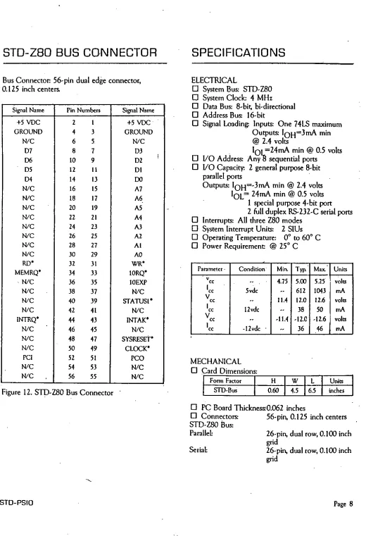
STO-Z80 8US CONNECTOR
Bus Connector: 56-pin dual edge connector,
0.125 inch centers.
Signal Name Pin Numbers Signal Name
+5 VOC 2 I +5
VOC-GROUND 4 3 GROUND
NlC
6 5NlC
07 8 7 OJ
D6 10 9 D2 i
05 12 11 Dl
04 14 13 DO
N/C
16 15 A7NlC
18 17 A6NlC
20 19 AS _.NlC
22 21 A4NlC
24 23 A3NlC
26 25 A2NlC
28 27 AlNlC
30 29 AORD' 32 31 WR'
MEMRQ' 34 33 IORQ'
- NlC
36 35 IOEXPNlC
38 37NlC
NlC
40 39 SfA11JSI'NlC
42 41NlC
INTRQ' 44 43 INfAK'
NlC
46 45N/C
NlC
48 47 SYSRESET'NlC
50 49 CLOCK'PCI 52 51 PCO
Nle
54 53NlC
Nle
56 55Nle
Figure 12.
STD-ZEOBus Connector
'
-STO-PSIO
SPECIFIC ATIONS
ELECTRICAL
o
System Bus:
STD-ZEO4 MHz
o
System Clock:
o
Data Bus: 8-bi
t,bi-directional
6-bit
o
Address Bus: I
o
Signal Loading: Inputs: One 74LS maximum
Outputs: IOH=3mA min
@
2.4 volts
o
VO
Address:
o
VO
Capacity:
para
lie!
portsIOL =24mA min
@0.5 volts
Any 8 sequential
ports2 general purpose 8-bit
=-3mA min
@2.4 volts
Outputs: IOH
IOL= 24mA min
@0.5 volts
1 special purpose 4-bit
port0
Interrupts: AU
2 full duplex RS-232-C serial
portsthree
ZEOmodes
o
System litterru pt Units: 2 SIUs
o
Operating Te mperature: 0° to 60° C
o
Power Require ment:
@25° C
Parameter· Co ndition' Min. Typ. Max. Units
vee 4.75 5.00 5.25 volts
Icc 5 vde 612 1043 rnA
V ee 11.4 12.0 12.6 yolts
Icc 1 2vde 38 50 rnA
Vee -11.4 -12.0 -12.6 volts
lee -1 2vde 36 46 rnA
MECHANICAL
o
Card Dimensio
ns:Form Factor H W L Units
SfD-Bus 0.60 4.5 6.5 inches
0
PC Board Thic kness:0.062 inches
o
Connectors:
STD-ZSO
Bus:
Paralleh
Seriah
56-pin, 0.125 inch centers
26-pin, dual row, 0.100 inch
grid
26-pin, dual row, 0.100 inch
grid
Page 8
•
[image:10.602.35.555.60.821.2]•
N
..
•
;;
•
Q
Q
•
u
•
\" ~ .. :I: ,.
_ _ ~ _ _ ~IJ
....,
....,
D c
)
•
N
...
'M
..
,
..
,
go,
81 SMI·
•
" <
~
"~" ".,
;~''.
.. 3 t 2 "
!~(\I'·III
...
n I ~'V1SJON .(Ql~D 1 lao.7!1188
F,. ;
OIL' •• ~"I 4,
'
,~--
__ I'u,.» "".
.ill"I.!" ,,,,. Y" • ,,;IT _
' 4
"
0'
._. ,
" " . ,
"
---11-":;:
1 ,I....
[0'·
u.
r
c',
.ll., ...,'u"'!..-::1
" "(QTSA~+
' ...
'~",ffl',...CC'::;,g:. ~~~'--::=-<"
[ ....
.19i..
'"
"
...r:::::-.;r~.
~ ~
(, I
L.'
.It -r't-
r'"
01 TXDA I '-<,00" • •
~-
" ..--
'~",
J .
IV'~/
• A IDTR)cD-tto
.
-
,,-
..
-
-
"'"
"
.
"~.:
, -
""
~"
o~,
..
Irr~~~~~~~~$ij~3'~~'
. -..: '.
~~
...
0"
""'"-<>I
.1 5
M ,
De U 13 R9~
2
J8 *I. , ,!6L _ _ _ _ _ _--'-""_~
U7 I a01 4 01 0 5 UI4-"
',... p
e
.
Z853 " .~;L:!1:~~___.!"'< ~}!...'---~'.:
..
:"~.:~~
.•
.
I· ....
"
sec "".
_ ., ..
~
• x
~
I.. "
'. -
~
-
, .
U8{~m
--,;;
~.
...
.;0'""""J,
PC'" ...
~
._- -
,
.r~-~
•
"'I:=- ".,
:;:.
I .
0" '
" ,
.. PC
~'.
.. _ A " _ .~.
" ' "
"d'
[
-"'''~-''
" ' .-~.
OIl ....~."""'"
I-; '" ",,'\- llu
aD,"
0,.,
II
.'
,
"
•"{~"
" ' ,_ """
"...,
[~~~u
,"
..
~=='
:'
:
~~=:::jI',,:::
' ' ' '
"",,-
-
-
-',,--
~
A . _-.
- . .
"
~..
"ou ...
__ .... ,
_
_
- . . .
~
DOu'·'
PA,.. ,
'~
...
I .. ••."'" , ,..
-,...,..
uoa..
r::'
..
-
,~~-
- " ,
..
...
,..
,
-
' . '" ,
• h '
" " "
+'1' .d!., ...J
r
iii! :
?':r:
...J:ffi:<l
~
"""f:l,""
-<:1 '"'
Yr
, , ", ;'
;..2..l
,
':!i,
....j:: :
..J -,"-<" ,II~
..
)to ItO PI!I_' ,'g;.' ;
"
'1"
~
+_
0 1)8 .... '8" , ' -
" .
'....
'- -
~
A . C:
~.
'" :: --,'~
...~:.
I " _ ,~
..(
. rEo...-
--!;
.
.~
,.
II!I JIC~
.
,,,lI\'!
.... PO.,'
"!~
';::'M ..~:; ~Iaa
.
.
;0.-1.-
~'-_~J
,
~,
"J
Dr>. 7 P",;""
~~~" ~i.
•
, ._
_"
--(. r-
-j;
...
~
' U ' < • ....~
: 114!
..
..:
..
,--.,
.
r:..
..
: ::::::::"_ '
J~
"''''C'
-:-, ..."""
: :
" u',
r,...
;--::v :
A
'TE~
8 Cf
•
o
c
8
..
~
,
~.
, ... ,....
CIII.e<_
L
____
j:~t:;j}
....
'.:U;_~
r-"
_ .
5<0- - - i IA
" ' . STOP
".
..
-
..
''"'-;;;;;;;~'O
•
1 D " -I~~ ~ _n.---r ... '"_~!
..
J _
6.,
II!Q,I\ Sltl_ cn. ...
7·04-o01REVA
-.
-04-000
-
"lMn 1-.. ____ ---rliitiT-Co 01'3 2