United States Patent (19)
11
Patent Number:
4,933,829
hite
45 Date of Patent:
Jun. 12, 1990
54 FREE RUNNING FLYBACK DC POWER 4,224,659 9/1980 Iguchi... 363/20 SUPPLY WITH CURRENT LIMIT CIRCUIT 4,272,806 6/1981 Metzger ... 363/21 4,323,961 4/1982 Josephson ... 363/56 75 Inventor: Alan V. White, Hockley, Tex. 4,425,611 1/1984 Easter ... 363/21
4,494,178 l/1985 Ishima ... 363/21
73) Assignee: Compaq Computer Corporation, 4,668,905 5/1987 Schierjott ... 363/56 X
Houston, Tex. 4,769,752 9/1988 Rackowe ... 363/56
Appl.
21 Appl. No.: 338,452 Primary Examiner-Peter S. Wong
(22 Filed: Apr. 17, 1989 Assistant Examiner-Emanuel T. Voeltz
Attorney, Agent, or Firm-Arnold, White & Durkee
Related U.S. Application Data 57 ABS CT
63 Continuation of Ser. No. 175,640, Mar. 24, 1988, aban- 57
doned, which is a continuation of Ser. No. 57,098, Jun. The present invention relates to a DC power supply of
2, 1987, abandoned. the free-running flyback type and a current limit circuit 511 Int. Cl... HO2M 3/24 incorporated therein. The current limit is changed as a
52 U.S. C. ... 363/95.363/21
function of AC line voltage thereby reducing the worst
363/131; 363/56; 361/91; 361/111 case peak power dissipation in the power switching
58 Field of Search ... 363/20, 21, 95, 97, transistor. In one embodiment, one or more turns on the
363/131, 55, 56, 57, 58: 361/91, 11, 18, 93 A s s s s s A y s transformer provides a sensing voltage proportional to f id 1 w l 56) References Cited supply voltage to vary the switching transistor current
U.S. PATENT DOCUMENTS
4,104,714 8/1978 Smith et al. ... 363/21
limit as a function of supply voltage.
8 Claims, 4 Drawing Sheets
NEOP 5 s
sw
----15S
-well----0PR
00P
Fw To -SS
4,933,829
Jun. 12, 1990
Sheet 1 of 4
U.S. Patent
Sheet 2 of 4
4,933,829
Jun. 12, 1990
U.S. Patent
4,933,829
1.
FREE RUNNING FLYBACK DC POWER SUPPLY
WITH CURRENT LIMIT CIRCUIT
This is a continuation of application Ser. No. 175,640,
filed Mar. 24, 1988, now abandoned, which is a continu
ation of application Ser. No. 057,098, filed June 2, 1987, now abandoned.
BACKGROUND OF THE INVENTION
I. Field of the Invention
This invention relates to a power supply for driving an electronic load.
II. Description of the Prior Art
Off-line switching mode power supplies are com
monly used in computers to achieve small size and high efficiency. The 115/230 Volts (AC) input power is rectified and passed through a regulating DC-DC con
verter to produce the various voltages needed for logic networks, disk drives, etc. A type of regulating con
verter in common use is the flyback or ringing choke type that stores energy in a multi-winding choke (power
transformer) during the first half cycle and delivers this energy to the output load during the second half cycle.
The storage and discharge portion of the duty cycle are generally controlled by a power transistor which acts as a switch. A common form of this flyback topology is
the discontinuous flyback topology, in which the choke magnetic field is allowed to collapse completely after
the second half cycle before a new cycle starts, leaving
no energy stored in the choke. Two forms of discontin
uous flyback topology are constant frequency, in which
the cycle is started at regular fixed intervals, and free running, in which the new cycle starts immediately
after the previous half cycle ends.
The power transistor used to switch the stored en
ergy in the choke has a large peak power dissipated in
the during the time required for transistor turnoff. In this short time, the peak power is dissipated near the
surface of the transistor silicon chip and, if high voltage
is present, on a small part of the surface. This dissipation of energy results in high peak temperatures and can
produce a runaway condition in the silicon called sec
ond breakdown which usually destroys the transistor.
This second breakdown limitation has resulted in spe
cial designs for high voltage switching power transis
tors and in snubber circuits to limit the rate of rise of
voltage across the switching transistor during turnoff. High voltage across a transistor concentrates the cur
rent flow and causes a higher spot temperature. The
snubber circuit allows the transistor to reach lower current before high voltage appears across the transis
tO.
RELATED APPLICATIONS
This application incorporates by reference copending application Ser. No. 057,535, filed concurrently here with, entitled "DC Power Supply With Digitally Con
trolled Power Transistor Switch' by Alan E. Brown.
BRIEF SUMMARY OF THE INVENTION
It has been found to be advantageous to limit the current of the power transistor before turnoff to prevent destruction by the second breakdown conditions during turnoff. The present invention provides an improved current limit circuit for this purpose.
For power supplies with current limiting features the choke inductance is selected to set the power capacity
O 15 20 25 30 35 45 50 55 65 2
of the power supply, at the operating frequency, at the
minimum supply voltage. The current should be large
enough to supply the desired power to the load, i.e.,
computer, yet small enough to avoid the second break down conditions. In constant frequency flyback topol ogy, the current required at turnoff does not change with a change in supply voltage. The effect of a higher
supply voltage is simply a shorter time for current to ramp up. In a free running flyback topology, this
shorter current ramp up time results in a frequency increase, reducing the peak current required to produce
the required power. Thus the frequency increase inher ent in a free running flyback topology results in lower required peak currents, a feature which is considered
advantageous. This characteristic further makes it pos sible to reduce the worst case stresses on the power
transistor by reducing the current limit threshold for higher supply voltages.
The present invention changes current limit as a func
tion of supply voltage by summing the voltage repre
senting the sensed collector current of the power tran sistor with a voltage representing the supply voltage.
The current limit circuit of the present invention gives
a relatively flat maximum power curve over the normal
range of supply voltage range and reduced power at supply voltages above this normal range. Line tran sients which may drive the supply voltage above the
normal maximum may cause a reduced power output,
however, the result of the reduced power output is a power supply shutdown.
A beneficial aspect of the present invention is that the
stresses normally imposed on power transistors during normal operation are reduced by controlling the cur rent limit threshold as a function of the supply voltage. An additional beneficial aspect of the present invention is that the control of the current limit threshold further limits the stresses on power transistors during line tran sient conditions, and results in reduced power output thus causing power supply shutdown. Although the
power supply shutdown, during abnormal supply volt age conditions, may cause some inconvenience, this is
viewed as minimal since the alternative would be a greater risk of power supply failure.
It is another object of the present invention to pro
vide a more reliable power supply by reducing stresses
on the power transistor by using some of the inherent characteristics of a free-running flyback topology and controlling, the maximum power supply output at
higher supply voltages. Control of the maximum power supply output thus results in lower transistor stresses.
It is a further object of the present invention to pro vide a power supply with a relatively constant output capacity over the normal range of supply voltages which reduces the output capacity at supply voltages above the normal range.
It is another object of the present invention to limit the current through the power transistor before turnoff
to prevent transistor damage from second breakdown
conditions during power transistor turnoff.
It is a further object of the present invention to pro vide increased power supply ruggedness for voltage supply transients without the cost of a larger power
transistor.
4,933,829
3
BRIEF DESCRIPTION OF THE DRAWINGS
FIG. 1A is a schematic diagram of the primary por tion of a first embodiment of this invention;
FIG. 1B is a schematic diagram of the primary por
tion of a second embodiment of this invention;
FIG. 2 is a partial schematic diagram of the second ary portion of both embodiments of the present inven
tion which are electrically connected within a power supply;
FIG. 3 is a plot which illustrates safe operating area margins for various collector currents as a function of
supply voltage and the switching transistor SOAR
limit;
FIG. 4 is a plot illustrating power supply output as a
function of supply voltage, with the effect of the present
invention on the power supply output illustrated in dashed lines.
DESCRIPTION OF THE PREFERRED EMBODIMENT
Referring now to FIGS. IA and 2, the present inven tion will be described in greater detail with reference to the schematic diagrams of a first embodiment. An un
regulated DC supply voltage is provided in the conven
tional manner by full-wave bridge rectifier (diode bridge) U4. Filtered AC voltage may be provided to the
AC side of the diode bridge U4 through power on-off
switch SW1, fuse F1 and one or more stages of LC line filter LF. Diode bridge U4 provides unregulated DC voltage to the primary windings of power transformer T1 (see FIG. 2). Electrically coupled in series with the
primary winding 21 of transformer T1 is switching transistor Q1. When Q1 is on, current flows in the pri mary winding 21, creating a magnetic field, thus storing
energy in transformer T1. When Q1 is switched off, the magnetic field collapses thus the energy initially stored in transformer T1 is transferred to the secondary wind ing of transformer T1, i.e., flyback is initiated. The switching action of Q1 is determined by an appropriate control signal at the base of Q1 from control transistor Q3. When transistor Q3 conducts, the base of Q1 is effectively connected to negative rail 22 thus turning off Q1. This initiates the transfer of energy stored in trans
former T1 to its secondary winding.
In prior art devices the resistor RC provides a voltage at the base of Q3 which is proportional to the current flowing through transistor Q1. Rc is tied between the
base Q3 and the negative rail 22 through the parallel
combination of resistors R9, R10, R11, R12, R13, and R14. In a first embodiment of the present invention, resis
tor RCL is electrically connected between positive rail
voltage at supply terminal 23 and the base of Q3. Resis tor RCL is preferably about 100K Ohms with a 5-watt
power rating. Also coupled to the based of Q3 is resistor
RC as described above for prior art devices.
Thus, the currents through RCL and Rc are summed at the base of Q3. Note that RCL and Rc are connected in series through parallel combination of R9 through R14 across the unregulated voltage of diode bridge U4 as indicated by V. When the base-emitter junction of Q3 is forward biased sufficiently, Q3 turns "on' thus initiating flyback. Without resistor RCL the base voltage of Q3 is directly proportional to the current through Q1 (i.e., as in prior art devices); however, with resistor RCL in the present invention, RCL is connected to the positive rail and serves to provide a voltage to the base
of Q3 which is proportional to the positive rail voltage.
10 15 20 25 30 35 45 50 55 60 65 4.
In the preferred embodiment the current through RCL
and current through Rc are summed at the base of Q3.
By connecting RCL in the manner illustrated in FIG.
1A, the voltage applied to the base of Q3 is a function of
the supply voltage (due to RCL) and the current
through Q1 (due to RC). Thus the turn "on' of Q3 can be affected by both variations in supply voltage (i.e., line transients) and the Q1 current (i.e., short circuit
conditions).
Under normal operating conditions current through Rcramps up to provide the turn-on voltage for Q3 over
a period of time in a fashion well known in the art. With the presence of RCL in the preferred embodiment, a higher supply voltage causes Q3 to turn on prematurely
(i.e., at a lower value of Q1 current). With higher supply
voltages present transistor Q3 turns-on quicker since resistor RCL provides a portion of the Q3 turn-on volt age. Thus a ramp-up function is provided through resis tor R but Q3 "turn-on' is offset by a value which is
proportional to the increased supply voltage. With the offset provided by RCL, Q3 is turned on sooner for higher supply voltages. Trimming resistor RT permits adjustment, during final assembly of the power supply,
to accommodate variations in Q3 characteristics (such
as hFe and VBE).
Power supply output voltages are generated in the conventional manner by diodes CR21A, CR21B,
CR22A, CR22B and CR29 and their associated filter
circuits as shown in FIG. 2. Capacitor C56 provides capacitive coupling between input and output ground. In general, the current through power switching transistor Q1 is allowed to reach a preset maximum
prior to turnoff. This current maximum is set to prevent
transistor damage and further reduced for lower trans
former power input to accomplish output voltage regu
lation. The turnoff of Q1 is normally accomplished by turn on of Q3. At Q1 turnoff, the inductance of the
primary winding 21 prevents a quick reduction of cur
rent, thereby causing a rapid rise in voltage across Q1. Without appropriate snubber and clamp circuits the result would normally be operation of transistor Q1 at a
combination of voltage and current outside the safe operating area (SOAR) with resulting transistor dam
age. With snubber and clamp circuits, the voltage rises at a volts/microsecond rate equal to snubber capacitor amps/microfarad. The snubber and clamp circuits allow safe operation as long as the current at Q1 turnoff
is not excessive.
Referring now to FIGS. IA and IB the function of
the snubber circuit and clamping circuit components
will be described in more detail. Capacitors C1 and C2 function in the flyback topology illustrated in a manner
well known in the art.
Again referring to FIGS. 1A and 1B, capacitor C45 and diode CR11 cooperatively operate with capacitors C5 and diode CR10 to provide a snubber circuit (also referred to as slew rate limit circuit which limits rate of rise of the collector voltage Q1), and collector voltage
clamp, respectively, during Q1 turnoff (i.e., flyback
cycle).
Due to the high inductance of the primary winding 21 of transformer T1 at Q1 turnoff conditions, the cur rent continues to flow thereby rapidly increasing V of Q1. As the voltage rises, current flows into C45 to limit the rate of rise of voltage. Although the current into C45 limits the rate of voltage rise (slew rate), the volt age would reach an excessive value if not clamped by
4,933,829
5
voltage positive rail and the additional 80 volts stored in
C5. Whenever the Q1 collector voltage rises 80 volts
higher than the supply voltage, at Q1 cutoff conditions,
CR10 becomes forward biased and conducts to carry
the excess transformer primary winding current into
C5.
Once the collector voltage is successfully clamped and Q1 is once again turned on, C45 discharges and C5
discharges to its steady-state value (i.e., VS-80 V)
through bleeder resistor R6 since both CR10 and CR11 are turned off when Q1 is forward biased.
The snubber circuit and the clamp circuit of the prior
art in combination with lower collector currents pro
duced by the supply voltage feed-forward circuit of the
present invention produces the curves illustrated in
FIG 3.
The slope of the curves is established by the slew rate
limiter with the turnoff (indicated in the curves) pro
vided by the clamp circuit. The ordinate of the graph
(collector amps) is controlled by the present invention
limiting collector current through varying supply volt
ages by providing a feed-forward voltage, which is a function of Vs to the base of Q3.
Implementation of the present invention permits a selection of collector "amps' with relative precision. Thus a designer can predict the stresses which will be imposed on Q1 by selection of the "collector amps.”
FIG. 1B illustrates a second embodiment of the pres
ent invention. Reference numerals illustrated in FIG. 1B are the same for similar components shown in FIG.
1A. The description for FIG. 1A for similar compo nents is incorporated herein by reference. In lieu of the resistor RCL as a means of sensing supply voltage to apply a proportional voltage to the base of Q3, a one turn sensing winding T and resistor R is used. The one-turn sensing winding T may be a single turn through the center of the donut shaped flyback trans former core or a single turn wound on to the primary of transformer T1 such that a voltage is developed in turn
T which is proportional to supply voltage V. This proportional voltage flows in resistor Ry which, as be
fore, develops a proportional voltage which is applied to the base of Q3 and which is summed with the voltage developed by the current flowing through transistor Q1
through resistors R9 through R14 and resistor RC. At
high supply voltages, a higher voltage is induced in the one turn sensing winding which in turn develops a higher voltage at the base of Q3 turning Q3 on sooner
during current ramp up. This results in a lower current limit on Q1 since it is turned off sooner on ramp up of
Q3.
A table of the values for the electrical components
used in the schematics shown in FIGS. 1A, 1B, and 2 is
set forth in Appendix A which is incorporated herein by
reference as if set forth in full.
FIG. 4 is a plot which demonstrates the effect of implementing the present invention. Note that, for a 100 volt rise in DC supply voltage, there is roughly a one amp reduction in peak current (from fixed peak current) in the normal operating range of approximately seven to nine amps. The results set forth in FIG. 4 demonstrate one of the novel aspects of the present invention in that power capacity remains relatively constant for supply voltage increases. This is in contradiction with prior art devices which have a power increase for supply voltage increases. Thus by effectively reducing power for sup ply voltages increases the stresses imposed on Q1 can be controlled. These novel aspects of the present invention
O 15 20 25 30 35 40 45 50 55 60 65 6
result in a more reliable power supply through the range of supply voltages and provide an added degree of reliability during transient overvoltage conditions.
Referring again to FIG. 4, the effect on power capac
ity of increasing supply voltage is reflected in solid lines, i.e., power output increases as a function of supply voltage without the supply voltage feed-forward circuit
consisting of resistor RCL (shown in FIG. 1A) or supply
voltage feed-forward circuit consisting of one-turn sensing winding T and resistor Rw (shown in FIG. 1B).
The flyback transformer primary power flowing
through Q1 increases as a function of supply voltage
and causes increased stresses on Q1 at elevated voltages.
Implementation of the supply voltage feed-forward circuit shown in FIG la and IB effectively reduces the flyback transformer primary current at elevated supply
voltages. The effect of this invention is show in dashed
lines. As supply voltage increases a decrease in current
results in nearly constant power input and consequently
output (efficiency remaining approximately equivalent)
and reduced Q1 stresses.
The principles, preferred embodiments and modes of operation of the present invention have been described in the foregoing specification. The invention is not to be construed as limited to the particular forms disclosed, since these are regarded as illustrative rather than re strictive. Moreover, variations and changes may be made by those skilled in the art without departing from the spirit of the invention.
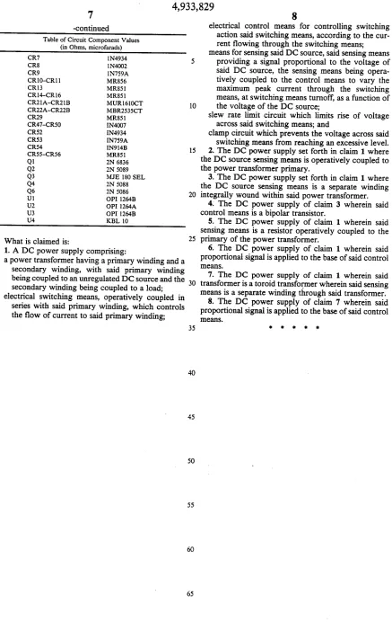
Table of Circuit Component Values (in Ohms, microfarads)
R1, R2 2.5
R3 360,2W
R4 22K, 2W R5 47K, 2W R6 2K, 22W R7 360, 2W
R8 22K, 2W R9-R14 2.2, 1/2W R22 20, 2W
R23 120
R24 OOK
R26 100K
R27 OK
R28 100K
R29 68K
R30 100K
R3 39, 2W
R109 1, 2W
Ry 9.
RC 22
RT 150
RCL 100K, 5W C1, C2 470, 250V
C3 .22
C4 1500, 20V C5 0.1, 500V
C6 22
C7 22
C8 O
CO .0
C12 68, 16V
Cl3 O47
C14 O
C16 3300, 20V C18 7700, 6.3V
C45 1800pf, 500V
C46 2.2, 25V
C56 0.2, 500V
C57 .22
C58 68, IOV
CR1-CR4 N914B
CR5 1N4934
4,933,829
7
[image:9.557.68.505.39.741.2]-continued Table of Circuit Component Values
(in Ohns, microfarads)
CR7 1N4934 5
CR8 1N4002
CR9 1N759A CR10-CR11 MR856
CR13 MR851 CR14-CR16 MR85
CR21A-CR21B MUR160CT 10
CR22A-CR22B MBR2535CT CR29 MR851
CR47-CR50 IN4007
CR52 IN4934 CR53 IN759A
CR54 IN914B 15
CR55-CR56 MR851
Q1 2N 6836 Q2 2N 5089 Q3 ME 180SEL Q4 2N 5088
Q6 2N 5086 20
Ul OP 1264B U2 OP 264A U3 OP 264B
U4 KBL 10
25
What is claimed is:
1. A DC power supply comprising:
a power transformer having a primary winding and a
secondary winding, with said primary winding
being coupled to an unregulated DC source and the 30
secondary winding being coupled to a load;
electrical switching means, operatively coupled in series with said primary winding, which controls
the flow of current to said primary winding;
35
45
50
55
65
8
electrical control means for controlling switching action said switching means, according to the cur
rent flowing through the switching means;
means for sensing said DC source, said sensing means providing a signal proportional to the voltage of
said DC source, the sensing means being opera
tively coupled to the control means to vary the maximum peak current through the switching
means, at switching means turnoff, as a function of the voltage of the DC source;
slew rate limit circuit which limits rise of voltage
across said switching means; and
clamp circuit which prevents the voltage across said
switching means from reaching an excessive level. 2. The DC power supply set forth in claim 1 where
the DC source sensing means is operatively coupled to the power transformer primary.
3. The DC power supply set forth in claim 1 where
the DC source sensing means is a separate winding
integrally wound within said power transformer.
4. The DC power supply of claim 3 wherein said control means is a bipolar transistor.
5. The DC power supply of claim 1 wherein said sensing means is a resistor operatively coupled to the primary of the power transformer.
6. The DC power supply of claim 1 wherein said proportional signal is applied to the base of said control
caS.
7. The DC power supply of claim 1 wherein said
transformer is a toroid transformer wherein said sensing means is a separate winding through said transformer.
8. The DC power supply of claim 7 wherein said proportional signal is applied to the base of said control
e2S.
UNITED STATES PATENT AND TRADEMARK OFFICE
CERTIFICATE OF CORRECTION
PATENT NO. : 4,933, 829
DATED
June 12, 1990
NVENTOR(S) :
White
It is Certified that error appears if the above-identified patent and that said Letters Patent
is hereby Corrected as shown below:
In column 8, line 2; please replace 'action said
switching' with --action of said switching --.
Signed and Sealed this
Sixteenth Day of July, 1991
HARRY F. MAN BECK, JR.