A STUDY ON ROADMAP FOR FUTURE MULTI GATE SOI MOSFET
Neeraj Gupta*, A.K. Raghav**, Janak B. Patel***
*(Asst. Prof. ,Amity School Of Engineering& Technology, Gurgaon,Haryana) **(Director, IRD Amity university Gurgaon,Haryana)
***(Prof. ,Amity School Of Engineering & Technology, Gurgaon,Haryana)
ABSTRACT
As the device dimension decreases
continuously, the speed of operation and
packaging density of MOSFET increases but
it reduces the device performance in terms
of short channel effect, parasitic
capacitances and leakage current. At
present, the single gate SOI MOSFET is
reaching its scaling limit. In this paper single
gate to multiple gate SOI MOSFET are
covered along with solutions to SCE based
on electrostatic integrity. So finally we have
to tradeoff between oxide thickness and
dielectric constant for better control over
channel by gate.
Keywords: Short channel effect (SCE),
Kink effect, Electrostatic integrity and
Natural length λ
I Introduction
MOSFETs are the basic building blocks of
microprocessors, memory circuits and
telecommunications microcircuits. But
future technology required high
performance, low operating power and low
leakage. The most efficient way to increase
the performance is to scale down
aggressively the gate length of the transistor,
since it allows reducing the channel
capacitance while on the other side
increasing the on-state current and reduced
the power.The downscaling of MOS
transistors increases in transistor density and
performance. While on the other side the
reduction in MOSFET dimensions leads to
the reduction in channel length between
source and drain, which in turn reduces the
control of the gate electrode to control the
current flow in the channel region and also
results in some undesirable effects known as
the channel effects (SCEs). The
short-channel effects become the barrier for
further scaling of conventional MOSFET.
downscaling of MOSFET give birth to
number of new innovative techniques which
include the use of different device
structures, different gate-metal materials,
different gate-oxide materials and different
processes.So we move further to multi-gate
device. The main advantage of the
multi-gate devices is the improved short channel
effects. The channel is controlled electro
statically by the gate from allsides; the
channel is better-controlled by the gate than
in the conventional SOI MOSFET structure.
There is no doubt for the manufacturers, if
they desire to scale the channel length and
catch–up with the International Technology
Roadmap for Semiconductor that they will
have to use multi-gate devices [1].
In this review paper, there are four sections.
Section I includes the introduction, Section
II described different devices structures,
Section III covered solutions to SCE based
on electrostatic integrity and Section IV
includes the conclusion and future work.
II Device Structures
Gordon Moore made an empirical
observation in 1965 that the number of
devices on a chip doubles in every 18
months [2]. Following Moore law various
MOSFET models designed. As the CMOS
technology scaling enters the nanometer
region, many serious problems called the
short channel effects comes into picture.
Hence there is a need of considering the new
device structures to suppress the short
channel effects. Figure 1 shows a schematic
view of a conventional bulk n-channel
MOSFET [3]. As the channel length L is
reduced to increase both the operating speed
and the packing density, the so-called
short-channel effects arise. The SCEs also causes
parasitic capacitances. So the solution of this
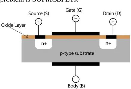
[image:2.612.324.543.323.472.2]problem is SOI MOSFETs.
Figure 1 A schematic view of a conventional
bulk n-channel MOSFET
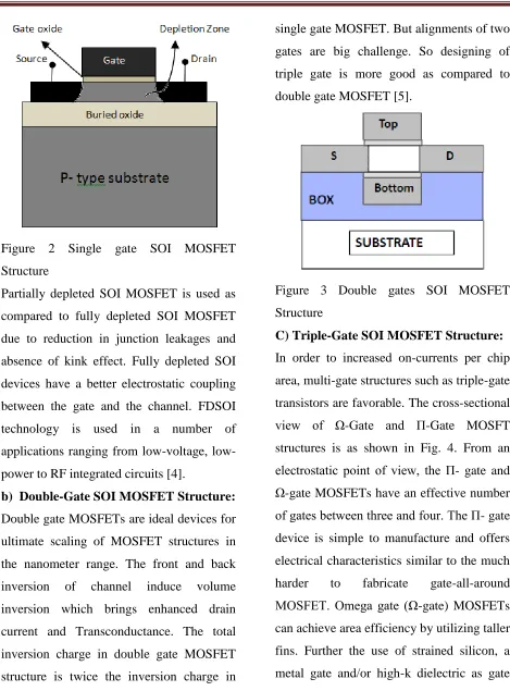
a)Single-Gate SOI MOSFET Structure:
In silicon on insulator (SOI) technology,
MOSFETs are realized in a thin layer of
silicon sitting on top of an insulator,
normally on SiO2, called “buried oxide”.
The thickness of silicon film typically
ranges between 50 and 200nm, while the
buried oxide thickness usually ranges
Figure 2 Single gate SOI MOSFET
Structure
Partially depleted SOI MOSFET is used as
compared to fully depleted SOI MOSFET
due to reduction in junction leakages and
absence of kink effect. Fully depleted SOI
devices have a better electrostatic coupling
between the gate and the channel. FDSOI
technology is used in a number of
applications ranging from voltage,
low-power to RF integrated circuits [4].
b) Double-Gate SOI MOSFET Structure:
Double gate MOSFETs are ideal devices for
ultimate scaling of MOSFET structures in
the nanometer range. The front and back
inversion of channel induce volume
inversion which brings enhanced drain
current and Transconductance. The total
inversion charge in double gate MOSFET
structure is twice the inversion charge in
single gate MOSFET. But alignments of two
gates are big challenge. So designing of
triple gate is more good as compared to
double gate MOSFET [5].
Figure 3 Double gates SOI MOSFET
Structure
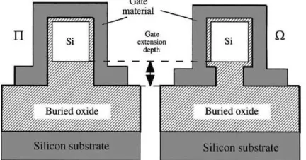
C) Triple-Gate SOI MOSFET Structure:
In order to increased on-currents per chip
area, multi-gate structures such as triple-gate
transistors are favorable. The cross-sectional
view of Ω-Gate and Π-Gate MOSFT
structures is as shown in Fig. 4. From an
electrostatic point of view, the Π- gate and Ω-gate MOSFETs have an effective number of gates between three and four. The Π- gate
device is simple to manufacture and offers
electrical characteristics similar to the much
harder to fabricate gate-all-around
MOSFET. Omega gate (Ω-gate) MOSFETs
can achieve area efficiency by utilizing taller
fins. Further the use of strained silicon, a
[image:3.612.71.540.68.703.2]insulator can further enhance the current
driving capability of the device. But square
gate all around MOSFET suffers from
undesirable effect known as corner effect.
The solution of this problem is cylindrical
[image:4.612.323.535.166.368.2]gate all around MOSFET [6-8].
Figure 4 Triple gate SOI MOSFET Structure
d) Surrounding-Gate (Quadruple-Gate)
SOI MOSFETs:
Among various multi-gate device structures,
the structure that theoretically offers the best
possible control of the channel region by the
gate is the surrounding-gate MOSFET.
The main advantage of the multi-gate
devices is the improved short channel
effects. Since the channel is controlled
electro statically by the gate from multiple
sides, the channel is better-controlled by the
gate than in the single and double gate
MOSFET structure.
The area occupied by surrounding-gate
MOSFET can be shrunk to less than 30% of
that occupied by the planar transistor. The
small occupied area leads to the small
junction capacitance and the small gate
electrode RC delay, resulting in high-speed
operation [9-10].
Figure 5 Surroundinggate SOI MOSFET
Structure
III Solutions to SCE based on electrostatic
integrity
Electrostatic Integrity (EI) base design
allows further scaling. The electrostatic
integrity describes the quality of the
electrostatic control of the channel by the
gate. Smaller the EI better the control of
gate over channel .Theimportant parameter
in achieving EI is natural length (λ).It can be
derived from Poisson's equation.The natural
length (λ)of a device represents the length of
the region of the channel that is controlled
by the drain. Natural length λ of various
[image:4.612.73.289.235.348.2]Single
Gate λ
Double
Gate λ
Triple
Gate λ
Quadruple
Gate λ
Surround
Gate
Consider natural length λ, given by
λ
To reduce λ, reduce oxide thickness and
silicon thickness and increase the value
of n and dielectricconstant . But reducing
oxide thickness can increase leakage current
due to direct tunneling. By increasing
dielectric constant the natural length λ
reaches its scalinglimit [11-13].
IV CONCLUSION AND FUTURE
WORK
The integrated circuit performance increases
exponentially with the scaling of
conventional MOSFET dimensions. The
scaling of SOI MOSFET transistors leads to
growth of semiconductor industry. In this
review paper all transistors from single gate
to multiple gates are discussed. The
solutions to SCE based on electrostatic
integrity are also described. EI indicates
how well the gate field controls the channel
field. Natural length suggests that reduction
in gate oxide thickness and silicon thickness
result in better EI. So we have to tradeoff
between oxide thickness and dielectric
constant. The ratio of oxide thickness and
dielectric constant is a better metric.So try to
make natural length λ should be as small as
possible for better control over channel by
gate.
References
[1] "The International Technology Roadmap
for Semiconductors," 2007.
[2] K P Pradhan, P K Agarwal, P K Sahu, S
K Mohapatra, “Role of highk materials in
Nanoscale TM-DG MOSFET: A simulation
study”, FirstNational Conference on Recent
Developments in Electronics (NCRDE),
New Delhi, January 18-20, 2013.
[3]S.M.Kang, CMOS digital integrated
[4] Jean-Pierre Colinge, Cynthia A. Colinge,
“Physics of Semiconductor Devices”,
Springer International Edition, 2002
[5] B. Agrawal, V.K. De, J.M. Pimbley, J.D.
Meindl, “Short channel models and scaling limits of SOI and bulk MOSFETs”, IEEE
Journal of Solid-State Circuits, vol. 29, no.
2, pp. 122-125, 1994
[6] V. Subramanian, “Multiple Gate
Field-Effect Transistors for Future CMOS
Technologies” IETE Tech. Review, vol. 27,
Issue 6, pp. 446-454, 2010
[7]Neeraj Gupta, A.K.Raghav and Alok K.
Kushwaha "A study on multi material gate
all around SOI MOSFET", International
Journal of Technological Exploration and
Learning ,VOL. 3,No.3,June 2014.
[8]Santanusharma and KabitaChaudhary,"A
novel technique for suppression of corner
effect in square gate all around MOSFET",
Journal of Electrical and Electronic
Engineering, VOL. 2 ,No.5, pp.
336-341,2012.
[9] A. Nitayama, H. Takato, N. Okabe, K.
Sunouchi, K. Hieda, F. Horiguchi, F.
Masuoka, “Multi-pillar surrounding gate
transistor (M-SGT) for compact and
high-speed circuits”, IEEE Transactions on
Electron Devices, vol. 38, no. 3, p. 579,
1991
[10] AbhinavKranti, S. Haldarb, R.S. Gupta,
“Analytical model for threshold voltage and
I–V characteristics of fully depleted short
channel cylindrical/surrounding gate
MOSFET” Microelectronic Engineering,
vol. 56 , pp. 241–259, 2001
[11] Sevinç Ozkara, Cryptographic
Techniques- Essential Applications In
Network Administration, Scholedge
International Journal Of Multidisciplinary &
Allied Studies, Vol.1,Nov.Issue;
www.scholedge.org, pp. 15-18,2014
[12] J.‐P. COLINGE, "The New Generation
of SOI MOSFETs", Romanian Journal of
Information Science and Technology, Vol.
11, Number 1, 2008, pp. 3‐15.
[13]Ran‐Hong Yan, Abbas Ourmazd, and
Kwing F. Lee, "Scaling the Si MOSFET:
From Bulk to SOI to Bulk",
IEEETransactions on Electron Devices,
VOL. 39, NO.7, JULY 1992.
[14]P.M. Zeitzoff, J.A. Hutchby and H.R.
Huff, MOSFET and Front-End Process
Integration: Scaling Trends, Challenges, and
Potential Solutions Through The End of The
Roadmap, International Journal of