N N C"')
a..
o
U...
,...
N C"')
a..
o
U...
QN C"')
a..
o
U...
NN
"'II:t
a..
o
U...
,...
N "'II:t
a..
o
U
...
Q
N "'II:t
a..
o
U~National
D
Semiconductor
COP420/COP421/COP422 and COP320/COP321/COP322
Single-Chip N-Channel Microcontrollers
General Description
The COP420, COP421, COP422, COP320, COP321 and COP322 Single-Chip N-Channel Microcontrollers are mem-bers of the COPSTM family, fabricated using N-channel, sili-con gate MOS technology. They are complete microcom-puters containing all system timing, internal logic, ROM, RAM and I/O necessary to implement dedicated control functions in a variety of applications. Features include single supply operation, a variety of output configuration options, with an instruction set, internal architecture and I/O scheme designed to facilitate keyboard input, display output and BCD data manipulation. The COP421 is identical to the COP420, except with 19 I/O lines instead of 23; the COP422 has 15 I/O lines. They are an appropriate choice for use in numerous human interface control environments. Standard test procedures and reliable high-density fabrica-tion techniques provide the medium to large volume cus-tomers with a customized Controller Oriented Processor at a low end-product cost.
The COP320 is the extended temperature range version of the COP420 (likewise the COP321 and COP322 are the ex-tended temperature range versions of the COP421/ COP422). The COP320/321/322 are exact functjonal equivalents of the COP420/421/422.
Block Diagram
Features
• Low cost
• Powerful instruction set • 1 k x 8 ROM, 64 x 4 RAM • 23 I/O lines (COP420, COP320) • True vectored interrupt, plus restart • Three-level subroutine stack • 4.0 ,.,.s instruction time • Single supply operation
• Internal time-base counter for real-time processing • Internal binary counter register with MICROWIRETM
compatible serial I/O capacity
• General purpose and TRI-STATE® outputs • TTL/CMOS compatible in and out • LED direct drive outputs • MICROBUSTM compatible
• Software/hardware compatible with other members of COP400 family
• Extended temperature range device COP320/COP321/ COP322 (-40°C to +85°C)
OJ
02
0,·
DO·
5 • 1 I 12 13 14 15
·Not available on COP322/COP422. TL/DD/6921-1
FIGURE 1
COP420/COP421/COP422 and COP320/COP321/COP322
Absolute Maximum Ratings
If Military/Aerospace specified devices are required, Package Power Dissipation 750 mW at 25·C contact the National Semiconductor Sales Office/ 24 and 28 pin 400 mW at 70·C Distributors for availability and specifications. 250 mW at 85·C Voltage at Any Pin -0.3Vto +7V Package Power Dissipation 650 mW at 25·C
Operating Temperature Range 20 pin 300 mW at 70·C
COP420/COP421/COP422 O·Cto 70·C 200 mW at 85·C
COP320/COP321/COP322 - 40·C to + 85·C Lead Temperature (soldering, 10 sec.) 300·C Storage Temperature Range - 65·C to + 150·C Absolute maximum ratings indicate limits beyond which
Total Sink Current 75mA damage to the device may occur. DC and AC electrical Total Source Current 95mA specifications are not ensured when operating the device at
absolute maximum ratings.
COP420/COP421/COP422
DC Electrical Characteristics
o·c :::;:
T A :::;: + 70·C, 4.5V :::;: Vee:::;: 6.3V unless otherwise notedParameter Conditions Min Max Units
Operation Voltage 4.5 6.3 V
Power Supply Ripple Peak to Peak (Note 3) 0.4 V
Supply Current Outputs Open 38 mA
Supply Current Outputs Open, 30 mA
Vee
=
5V, TA=
25·C Input Voltage LevelsCKllnput Levels Crystal Input
Logic High Vee
=
Max. 3.0Logic High Vee
=
5V ±5% 2.0 VLogic Low -0.3 0.4 V
TTL Input Vee
=
5V ±5%Logic High 2.0 V
Logic Low -0.3 0.8 V
Schmitt Trigger Inputs RESET, CKI (-:- 4)
Logic High 0.7 Vee V
Logic Low -0.3 0.6 V
SO Input Level (Test Mode) (Note 2) 2.0 3.0 V All Other Inputs
Logic High Vee
=
Max. 3.0 VLogic High Vee
=
5V ±5% 2.0 VLogic Low -0.3 0.8 V
Input Levels High Trip Option
Logic High 3.6 V
Logic Low -0.3 1.2 V
Input Load Source Current Vee
=
5V, VIN=
OVCKO -4 -800 /J-A
All Others -100 -800 /J-A
Input Capacitance 7 pF
Hi-Z Input Leakage -1 +1 /J-A
Output Voltage Levels Standard Outputs
TTL Operation Vee
=
5V ±10%Logic High IOH
=
-100/J-A 2.4 VLogic Low IOl
=
1.6 mA -0.3 0.4 VCMOS Operation (Note 1)
Logic High IOH
=
-10/J-A Vee -1 VLogic Low IOl
=
+10/J-A 0.2 VNote 1: TRI·STATE and LED configurations are excluded.
Note 2: SO output "0" level must be less than O.BV for normal operation.
1-113
o
"'0
0l:Io N C
...
o
o
"'0
0l:Io N
...
...
o
o
"'0
0l:Io N N
...
o
o
"'0
(,.)
N C
...
o
o
"'0
(,.)
N
...
...
o
o
"'0
(,.)
N N
N N
C")
a..
o
o
...
--NC")
a..
o
o
...
o
N
C")
a..
o
o
...
N N ~a..
o
o
...
--N ~a..
o
o
...
o
N ~a..
o
o
COP420/COP421/COP422
DC Electrical Characteristics
o·c
:5: T A :5: + 70·C, 4.5V :5: Vee :5: 6.3V unless otherwise noted (Continued)Parameter Conditions Min Max Units
Output Current levels
lED Direct Drive Output Vee
=
6Vlogic High VOH
=
2.0V 2.5 14 mACKI Sink Current (RIC Option) VIN
=
3.5V 2 rnACKO (RAM Supply Current) VA
=
3.3V 3 rnATRI·STATE or Open Drain Vee
=
5V -2.5+2.5 p.A leakage Current
Output Current levels
Output Sink Current (Iou Vee
=
4.5V, VOL=
0.4V +1.6 rnA Output Source Current (IOH)Standard Configuration
All Outputs Vee
=
6.3V, VOH=
3.0V -200 -900 p.A Vee=
4.5V, VOH=
2.0V -100 -500 p.A Push· Pull ConfigurationSO, SK Outputs Vee
=
6.3V, VOH=
3.0V -1.0 rnA Vee=
4.5V, VOH=
2.0V -0.4 rnA TRI·STATE ConfigurationLo-l7 Outputs Vee
=
6.3V, VOH=
3.2V -0.8 rnA Vee=
4.5V, VOH=
1.5V -0.9 rnA lED ConfigurationLo-l7 Outputs Vee
=
6.3V, VOH=
3.0V -1.0 rnA Vee=
4.5V, VOH=
2.0V -0.5 rnA Allowable Sink CurrentPer Pin (l, 0, G) 10 rnA
Per Pin (All Others) 2 rnA
Per Port (l) 16 rnA
PerPort(D,G) 10 rnA
Allowable Source Current
Per Pin (l) -15 rnA
Per Pin (All Others) -1.5 rnA
COP320/COP321/COP322
DC Electrical Characteristics
-40·C:S: TA:S: +B5·C,4.5V:S: Vee:S: 5.5VunlessotherwisenotedParameter Conditions Min Max
Operation Voltage 4.5 5.5
Power Supply Ripple Peak to Peak (Note 3) 0.4 Supply Current TA
=
-40·C, Outputs Open 40 Input Voltage LevelsCKllnput Levels Crystal Input
Logic High 2.2
Logic Low -0.3 0.3
TIL Input Vee
=
5V ±5%Logic High 2.2
Logic Low -0.3 0.6
Schrnitt Trigger Inputs RESET, CKI ( + 4)
Logic High 0.7 Vee
Logic Low -0.3 0.4
SO Input Level (Test Mode) (Note 2) 2.0 3.0 All Other Inputs
Logic High Vee
=
Max. 3.0Logic High Vee
=
5V ±5% 2.2Logic Low -0.3 0.6
Input Levels High Trip Option
Logic High 3.6
Logic Low -0.3 1.2
Input Load Source Current Vee
=
5V, VIN=
OVCKO -4 -800
All Others -100 -BOO
Input Capacitance 7
Hi-Z Input Leakage -2 +2
Output Voltage Levels Standard Outputs
TIL Operation Vee
=
5V ±10%Logic High IOH
=
-75 p,A 2.4Logic Low IOL
=
1.6 rnA -0.3 0.4CMOS Operation (Note 1)
Logic High IOH
=
-10 p,A Vee -1Logic Low IOL
=
+10 p,A -0.3 0.2Output Current Levels
LED Direct Drive Output Vee
=
5V (Note 4)Logic High VOH
=
2.0V 1.0 12CKI Sink Current (RIC Option) VIN
=
3.5V 2CKO (RAM Supply Current) VA
=
3.3V 4TRI-STATE or Open Drain -5 +5
Leakage Current Allowable Sink Current
Per Pin (L, 0, G) 10
Per Pin (All Others) 2
Per Port (L) 16
PerPort(D,G) 10
Allowable Source Current
Per Pin (L) -15
Per Pin (All Others) -1.5
Note 1: TAl-STATE and LED configurations are excluded.
Note 2: SO output "0" level must be less than 0.6V for normal operation.
1-115
Units V V rnA
V V
V V
V V V
V V V
V V
p,A p,A pF p,A
V V
V V
rnA rnA rnA p,A
rnA rnA rnA rnA
rnA rnA
o
-a
oIloo I\) Q...
o
o
-a
oIloo I\)....
...
o
o
-a
oIloo I\) I\)...
o
o
-a
w
I\) Q
...
o
o
-a
w
I\)....
...
o
o
-a
w
I\) I\)N N
C")
D.
o
o
"
,...
N
C")
D.
o
o
"
o
NC")
D.
o
o
"
N N "II:t'
D.
o
o
"
,...
N "II:t'
D.
o
o
"
o
N "II:t'D.
o
o
AC Electrical Characteristics
COP420/COP421/COP422
o·c ::;;
T A ::;; 70·C, 4.5V ::;; VCC ::;; 6.3V unless otherwise noted COP320/COP321/COP322 - 40·C ::;; T A ::;;+
85·C, 4.5V ::;; V cc ::;; 5.5V unless otherwise notedParameter Conditions Min Max Units
Instruction Cycle Time 4 10 J.Ls
Operating CKI Frequency +16 mode 1.6 4.0 MHz
+8 mode 0.8 2.0 MHz
CKI Duty Cycle (Note 1) 40 60 %
Rise Time Freq.
=
4 MHz 60 nsFall Time Freq.
=
4 MHz 40 nsCKI Using RC (Figure Be) +4 mode
Frequency R
=
15kn ±5%,C=
100pF 0.5 1.0 MHzInstruction Cycle Time (Note 5) 4 8 J.Ls
CKO as SYNC Input (Figure Bd)
tSYNC Figure3a 50 ns
Inputs: SI
tSETUP 0.3 J.Ls
tHOLO 250 ns
All Other Inputs
tSETUP 1.7 ,..,s
tHOLO 300 ns
Output Propagation Delay Test Conditions: 300 ns
RL
=
5 kn, CL=
50 pF, VOUT=
1.5V SOandSKtpd1 1.0 ,..,s
tpdO 1.0 ,..,s
CKO
tpd1 0.25 ,..,s
tpdO 0.25 ,..,s
All Other Outputs
tpd1 1.4 ,..,s
tpdo 1.4 ,..,s
MICROBUSTM Timing CL
=
100 pF, VCC=
5V ±5%.
Read Operation (Figure 4)Chip Select Stable before RD-tCSR 65 ns
Chip Select Hold Time for RD-tRCS 20 ns
RD Pulse Width-tRR 400 ns
Data Delay from RD-tRO 375 ns
RD to Data Floating-tOF 250 ns
Write Operation (Figure 5)
Chip Select Stable before WR-tcsw 65 ns
Chip Select Hold Time for WR-twcs 20 ns
WR Pulse Width-tww 400 ns
Data Set-Up Time for WR-tow 320 ns
Data Hold Time for WR-two 100 ns
INTR Transition Time from WR-twi 700 ns
Note 1: Duty cycle = tW1/(tW1 + two).
Note 2: See Figure 9 for additional I/O characteristics.
Note 3: Voltage change must be less than O.SV in a 1 ms period.
Note 4: LED direct drive must not be used. Exercise great care not to exceed maximum device power dissipation limits when sourcing similar loads at high temperature.
Note 5: Variation due to the device included.
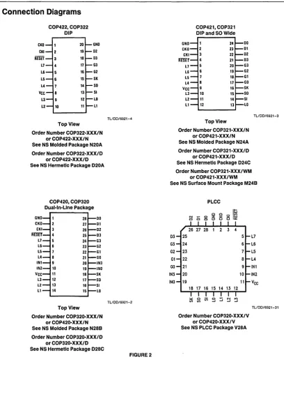
Connection Diagrams
COP422, COP322 DIP
eKO 20 GNO CKI 19 02 RESET 18 03 L7 17 G3 L6 16 02 L5 15 SK L4 14 SO Vee 13 SI L3 9 12 LO L2 10 11 Ll
Top View Order Number COP322-XXX/N
or COP422-XXX/N See NS Molded Package N20A Order Number COP322-XXX/D
or COP422-XXX/D See NS Hermetic Package D20A
COP420, COP320 Dual-ln-L1ne Package
GND DO
Dl D2 D3 G3 G2 Gl 21 GO IN3
17
LZ 13 16 L1 14 15
Top View Order Number COP320-XXX/N
or COP420-XXX/N See NS Molded Package N28B Order Number COP320-XXX/D
or COP320-XXX/D See NS Hermetic Package D28C
TL/DD/6921-4
[image:6.489.31.439.29.613.2]TL/DD/6921-2
FIGURE 2
1-117
COP421, COP321 DIP and SO Wide
DO
CKO 01
DZ 03
L7 G3
L6 G2
L5 Gl
L4 GO
Vee SK
L3 SO
L2 SI
L1 LO
Top View Order Number COP321-XXX/N
or COP421-XXX/N See NS Molded Package N24A Order Number COP321-XXX/D
or COP421-XXX/D See NS Hermetic Package D24C Order Number COP321-XXX/WM
or COP421-XXX/WM
TLlDD/6921-3
See NS Surface Mount Package M24B
03 G3 G2
Gl GO
IN3 INO
PLCC
L7 6 L6 7 L5 8 L4 INI 10 IN2 11 Vee
TL/DD/6921-31
Order Number COP320-XXX/V or COP420-XXX/V See NS PLCC Package V28A
o
"'C 0I:loo N
o
...
o
o
"'C 0I:loo N....
...
o
o
"'C 0I:loo N N...
o
o
"'C
w
N
o
...
o
o
"'C
W
N
....
...
o
o
"'C W N N
~
r---,
~C")
D..
o
o
...
...
~
C")
D..
o
[image:7.490.41.473.31.600.2]o
...
o
~
C")
D..
o
o
...
~ ~ "'1:1' D..
o
o
...
...
~ "'1:1' D..
o
o
...
o
~ "'1:1' D..
o
o
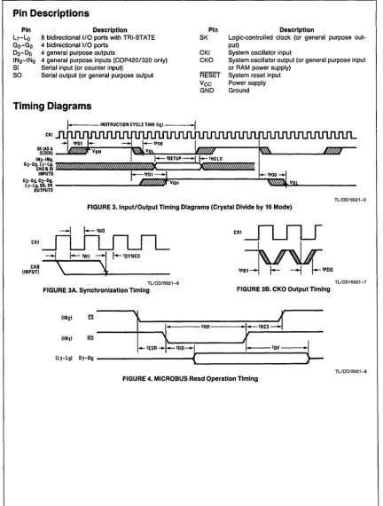
Pin Descriptions
Pin L7- LO
G3- GO
D3- 00
IN3-INo SI
so
Description 8 bidirectional 1/0 ports with TRI-STATE
4 bidirectional 1/0 ports
4 general purpose outputs
4 general purpose inputs (COP420/320 only) Serial input (or counter input)
Serial output (or general purpose output
Timing Diagrams
CKI
Pin SK
CKI CKO
RESET
Vee
GNO
S~~~M
1-~~----..&10""""111
IN3-INO.
I--
'SETUP- l
I-IHOLD
Description
Logic-controlled clock (or general purpose out-put)
System oscillator input
System oscillator output (or general purpose input or RAM power supply)
System reset input Power supply Ground
G3-GDck~&LRi
?!IUlffIIllflmlllm//uml//!!IUu/HIImIfUI/II/J/$
X'lUU/UIUllfuu/IU!l/I/UM
INPUTS ~IPD1-1
Gr;~~~~~~~~
InIl'l'lVlJl"''I/'''''rh~W,,'''rJ6~v~OH---
...
~':''''''
...
-OUTPUTS
FIGURE 3. Input/Output Timing Diagrams (Crystal Divide by 16 Mode)
- - I I - t W O
CKI
-I
I-
tW1j
1--
tSYNCO CKO \(INPUT) \. _ _ _ _ ... _ _ _ _ _ _ _
TL/DD/6921-6
FIGURE 3A. Synchronization Timing
,
C K I J L F L r
1
I
'PD~'PDD
FIGURE 3B. CKO Output Timing1
tRR • -tRCS-:::j
~.
,
-- tCSR
--f.-
tRD-1 I - - t D F.
(lNd RD
IL1-LO) D1- DO
---'1("'-____________
~
FIGURE 4. MICROBUS Read Operation Timing
1-118
TL/DD/6921-5
TL/DD/6921-7
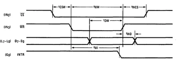
Timing Diagrams
(Continued).I-ICSW-- • IVIW
• -twcs-I
\
1
I I O W
-'(
-
two
.1-'(
X
.
twl
..
(Go) INTR
[image:8.487.79.401.50.159.2]TL/DD/6921-9
FIGURE 5. MICROBUS Write Operation Timing
Functional Description COP420/COP421/COP422,
COP320/COP321/COP322
For ease of reading this description, only COP420 and/or COP421 are referenced; however, all such references apply equally to the COP422, COP322, COP320 and/or COP321, respectively.
A block diagram of the COP420 is given in Figure 1. Data paths are illustrated in simplified form to depict how the vari-ous logic elements communicate with each other in imple-menting the instruction set of the device. Positive logic is used. When a bit is set, it is a logic "1" (greater than 2V). When a bit is reset, it is a logic "0" (less than O.BV). PROGRAM MEMORY
Program Memory consists of a 1,024 byte ROM. As can be seen by an examination of the COP420/421 instruction set, these words may be program instructions, program data or ROM addressing data. Because of the special characteris-tics associated with the JP, JSRP, JID and LQID instruc-tions, ROM must often be thought of as being organized into 16 pages of 64 words each.
ROM addressing is accomplished by a 10-bit PC register. Its binary value selects one of the 1,024 8-bit words contained in ROM. A new address is loaded into the PC register during each instruction cycle. Unless the instruction is a transfer of control instruction, the PC register is loaded with the next sequential 10-bit binary count value. Three levels of subrou-tine nesting are implemented by the 10-bit subrousubrou-tine save registers, SA. SB and SC, providing a last-in, first-out (LIFO) hardware subroutine stack.
1-119
ROM instruction words are fetched, decoded and executed by the Instruction Decode, Control and Skip Logic circuitry. DATA MEMORY
Data memory consists of 256-bit RAM, organized as 4 data registers of 16 4-bit digits. RAM addressing is implemented by a 6-bit B register whose upper 2 bits (Br) select 1 of 4 data registers and lower 4 bits (8d) select 1 of 16 4-bit digits in the selected data register. While the 4-bit contents of the selected RAM digit (M) is usually loaded into or from, or exchanged with, the A register (accumulator), it may also be loaded into or from the Q latches or loaded from the L ports. RAM addressing may also be performed directly by the LDD and XAD instructions based upon the 6-bit contents of the operand field of these instructions. The Bd register also serves as a source register for 4-bit data sent directly to the D outputs.
INTERNAL LOGIC
The 4-bit A register (accumulator) is the source and desti-nation register for most 110, arithmetic, logic and data mem-ory access operations. It can also be used to load the Br and Bd portions of the B register, to load the input 4 bits of the 8-bit Q latch data, to input 4 bits of the B-bit L 110 port data and to perform data exchanges with the SID register.
o
-a
~ NQ
...
o
o
-a
~ N -a....
o
o
-a
~ N N...
o
o
-a
w
N
Q
...
o
o
-a
w
N -a.
...
o
o
-a
w
N r---~ N
C")
D-o
o
...
,...
N
C")
D-O
o
...
o
NC")
D-O
o
...
N N
'OI:t'
D-O
o
...
,...
N
'OI:t'
D-O
o
...
o
N
'OI:t'
D-O
o
Functional Description COP420/COP421/COP422,
COP320/COP321/COP322
(Continued)A 4-blt adder performs the arithmetic and logic functions of the COP420/421, storing its results in A. It also outputs a carry bit to the 1-bit C register, most often employed to indicate arithmetic overflow. The C register, in conjunction with the XAS instruction and the EN register, also serves to control the SK output. C can be outputted directly to SK or can enable SK to be a sync clock each instruction cycle time. (See XAS instruction and EN register description, be-low.)
Four general-purpose Inputs, IN3-INQ, are provided; IN1, IN2 and IN3 may be selected, by a mask-programmable op-tion, as Read Strobe, Chip Select and Write Strobe inputs, respectively, for use in MICROBUS applications.
The 0 register provides 4 general·purpose outputs and is used as the destination register for the 4-bit contents of Bd. The G register contents are outputs to 4 general-purpose bidirectional 1/0 ports. Go may be mask-programmed as an output for MICROBUS applications .
The Q register is an internal, latched, 8-bit register, used to hold data loaded to or from M and A, as well as 8-bit data from ROM. Its contents are output to the L 1/0 ports when the L drivers are enabled under program control. (See LEI instruction.) With the MICROBUS option selected, Q can also be loaded with the 8-bit contents of the L 1/0 ports upon the occurrence of a write strobe from the host CPU. The 8 L drivers, when enabled, output the contents of latched Q data to the L 1/0 ports. Also, the contents of L may be read directly into A and M. As explained above, the MICROBUS option allows L 1/0 port data to be latched into the Q register. L 1/0 ports can be directly connected to the segments of a multiplexed LED display (using the LED Di-rect Drive· output configuration option) with Q data being outputted to the Sa-Sg and decimal point segments of the display.
The 510 register functions as a 4-bit serial-in/serial-out shift register or as a binary counter depending on the con-tents of the EN register. (See EN register description, be-low.) Its contents can be exchanged with A, allowing it to input or output a continuous serial data stream. SIO may also be used to provide additional paralJelllO by connecting SO to external serial-in/paralJel-out shift registers. For ex-ample of additional parallel output capacity see Application #2.
The XAS instruction copies C into the SKL latch. In the counter mode, SK is the output of SKL; in the shift register mode, SK outputs SKL ANDed with the clock.
The EN register is an internal 4-bit register loaded under program control by the LEI instruction. The state of each bit of this register selects or deselects the particular feature associated with each bit of the EN register (EN3-ENo).
1. The least significant bit of the enable register, ENo se-lects the SIO register as either a bit shift register or a 4-bit binary counter. With ENo set, SIO is an asynchronous binary counter, decrementing its value by one upon each low-going pulse ("1" to "0" occurring on the SI input. Each pulse must be at least two instruction cycles wide. SK outputs the value of SKL. The SO output is equal to the value of EN3. With ENo reset, SIO is a serial shift register shifting let each instruction cycle time. The data present at 01 goes into the least significant bit of SIO. SO can be enabled to output the most significant bit of SIO each cycle time. (See 4 below.) The SK output becomes a logic-controlled clock.
2. With the EN1 set the IN1 input is enabled as an interrupt input. Immediately following an interrupt, EN1 is reset to disable further interrupts.
3. With EN2 set, the L drivers are enabled to output the data in Q to the L I/O ports. Resetting EN2 disables the L drivers, placing the L 1/0 ports in a high impedance input state.
4. EN3, in conjunction with ENo, affects the SO output. With ENo set (binary counter option selected) SO will output the value loaded into EN3. With ENo reset (serial shift register option selected), setting EN enables SO as the output of the SIO shift register outputting serial shifted data each instruction time. Resetting EN3 with the serial shift register option selected disables SO as the shift reg-ister output data continues to be shifted through SIO and can be exchanged with A via an XAS instruction but SO remains reset to "0". The table below provides summary of the modes associated with EN3 and EN1.
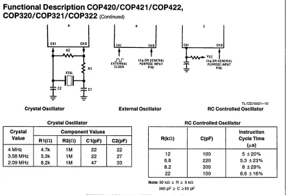
OSCILLATOR
There are three basic clock oscillator configurations avail-able as shown by Figure 8.
a. Crystal Controlled Oscillator. CKI and CKO are con-nected to an external crystal. The instruction cycle time equals the crystal frequency divided by 16 (optional by 8).
b. External Oscillator. CKI is an external clock input sig-nal. The external frequency is divided by 16 (optional by 8) to give the instruction cycle time. CKO is now avail-able to be used as the RAM power supply (VR) of as a general purpose input.
c. RC Controlled Oscillator. CKI is configured as a single pin RC controlled Schmitt trigger oscillator. The instruc-tion cycle equals the oscillainstruc-tion frequency divided by 4. CKO is available for non-timing functions.
Enable Register Modes-Bits EN3 and ENo
EN3 ENo 510 51 SO SK
0 0 Shift Register Input to Shift Register 0 If SKL = 1, SK = CLOCK If SKL = 0, SK = 0 1 0 Shift Register Input to Shift Register Serial Out If SKL = 1, SK = CLOCK
If SKL = 0, SK = 0 0 1 Binary Counter Input to Binary Counter 0 If SKL = 1, SK = 1 If SKL = 0, SK =
°
Functional Description COP420/COP421/COP422,
COP320/COP321/COP322
(Continued)uw
t;:t
J1..[" IVR OR GENERALCKI eKO
I ... .
Vcct
~
IVR OR GENERAL EXTERNAL PURPOSE INPUTI
PURPOSE INPUTRl CLOCK PIN)
-=-
PIN)XTAl
D
~C2
*ClCrystal Oscillator External Oscillator
TLlDD/6921-10
RC Controlled Oscillator
Crystal Oscillator Crystal Component Values
Value R1(O) R2(n) C1(pF) C2(pF)
4MHz 4.7k 1M 22 22 3.58 MHz 3.3k 1M 22 27 2.09 MHz 8.2k 1M 47 33
RC Controlled Oscillator
R(kO)
12 6.8 8.2 22
Note: 50 kfl ~ R ~ 5 kfl 360 pF ~ C ~ 50 pF
C(pF)
100 220 300 100
Instruction Cycle Time
(,...s) 5 ±20% 5.3 ±23%
[image:10.486.31.444.34.315.2]8 ±29% 8.6 ± 16%
FIGURE 8. COP420/4211COP320/321 Oscillator
CKO PIN OPTIONS
In a crystal controlled oscillator system, CKO is used as an output to the crystal network. As an option CKO can be a general purpose input, read into bit 2 of A (accumulator) upon execution of an INIL instruction. As another option, CKO can be a RAM power supply pin (VA)' allowing its con· nection to a standby/backup power supply to maintain the integrity of RAM data with minimum power drain when the main supply is inoperative or shut down to conserve power. Using either option is appropriate in applications where the COP420/421 system timing configuration does not require use of the CKO pin.
RAM KEEP-ALIVE OPTION (NOT AVAILABLE ON COP422)
Selecting CKO as the RAM power supply (VA) allows the user to shut off the chip power supply
(Vee>
and maintain data in the RAM. To insure that RAM data integrity is main-tained, the following conditions must be met:1. RESET must go low before
Vee
goes below spec during power off;Vee
must be within spec before RESET goes high on power up.2. VA must be within the operating range of the chip, and equal to
Vee
± 1V during normal operation.3.
VR
must be ~ 3.3V withVee
off. INTERRUPTThe following features are associated with the IN1 interrupt procedure and protocol and must be considered by the pro-grammer when utilizing interrupts.
a. The interrupt, once acknowledged as explained below, pushes the next sequential program counter address (PC
1-121
+
1) onto the stack, pushing in turn the contents of the other subroutine-save registers to the next lower level (PC+
1 ~ SA ~ SB ~ SC). Any previous con-tents of SC are lost. The program counter is set to hex address OFF (the last word of page 3) and EN1 is reset. b. An interrupt will be acknowledged only after the followingconditions are met: 1. EN1 has been set.
2. A low-going pulse ("1" to "0") at least two instruction cycles wide occurs on the IN1 input.
3. A currently executing instruction has been completed. 4. All successive transfer of control instructions and suc-cessive LBls have been completed (e.g., if the main program is executing a JP instruction which transfers program control to another JP instruction, the interrupt will not be acknowledged until the second JP instruc-tion has been executed.
c. Upon acknowledgement of an interrupt, the skip logic status is saved and later restored upon popping of the stack. For example, if an interrupt occurs during the exe-cution of ASC (Add with Carry, Skip on Carry) instruction which results in carry, the skip logic status is saved and program control is transferred to the interrupt servicing routine at hex address OFF. At the end of the interrupt
routine, a RET instruction is executed to "pop" the stack and return program control to the instruction following the original ASC. At this time, the skip logic is enabled
and skips this instruction because of the previous ASC carry. Subroutines and LQID instructions should not be nested within the interrupt service routine, since their
o
"tJ.I:Jo
I\)
o
...
o
o
"tJ
.I:Jo
I\) -&.
...
o
o
"tJ
.I:Jo
I\) I\)
...
o
o
"tJ (,) I\)
o
...
o
o
"tJ (,) I\) -&.
...
o
o
"tJ
(,)
I\) I\)
N N
C")
D.
[image:11.486.52.443.34.225.2] [image:11.486.260.452.205.580.2]o
o
...
--
NC")
D.
o
o
...
o
NC")
D.
o
o
...
N N "1:1'
D.
o
o
...
--N "1:1'D.
o
o
...
o
N "1:1'
D.
o
o
Functional Description COP420/COP421/COP422,
COP320/COP321/COP322
(Continued)POWER SUPPLY CLOCK
MICROPROCESSOR
~~~~~~ IN
OUT
TUDD/6921-12
FIGURE 6. MICROBUS Option Interconnect popping the stack will enable any previously saved main
program skips, interfering with the orderly execution of the interrupt routine.
d. The first instruction of the interrupt routine at hex ad-dress OFF must be a NOP.
e. A LEI instruction can be put immediately before the RET to re-enable interrupts.
MICROBUSTM INTERFACE
The COP420 has an option which allows it to be used as a peripheral microprocessor device, inputting and outputting data from and to a host microprocessor (,..,P). IN1, IN2 and INa general purpose inputs become MICROBUS compati-ble read-strobe, chip-select, and write-strobe lines, respec-tively. IN1 becomes RD-a logic "0" on this input will cause
Q latch data to be enabled to the L ports for input to the ,..,P. IN2 becomes CS-a logic "0" on this line selects the COP420 as the ,..,p peripheral device by enabling the opera-tion of the RD and WR lines and allows for the selecopera-tion of one of several peripheral components. IN3 becomes WR-a logic "0" on this line will write bus data from the L ports to the Q latches for input to the COP420. Go becomes INTR a "ready" output, reset by a write pulse from the ,..,p on the WR line, providing the "handshaking" capability necessary for asynchronous data transfer between the host CPU and the COP420.
This option has been designed for compatibility with Nation-al's MICROBUS-a standard interconnect system for a-bit parallel data transfer between MOS/LSI CPUs and interfac-ing devices. (See MICROBUS National Publication.) The functioning and timing relationships between the COP420 signal lines affected by this option are as specified for the MICROBUS interface, and are given in the AC electrical characteristics and shown in the timing diagrams (Figures 4 and 5). Connection of the COP420 to the MICROBUS is shown in Figure 6.
Note: TRI·STATE outputs must be used on L·port.
INITIALIZATION
The Reset Logic, internal to the COP420/421, will initialize (clear) the device upon power-up if the power supply rise time is less than 1 ms and greater than 1 ,..,s. If the power supply rise time is greater than 1 ms, the user must provide an external. RC network and diode to the RESET pin as
1-122
shown below. The RESET pin is configured as a Schmitt trigger input. If not used it should be connected to Vee. Initialization will occur whenever a logic "0" is applied to the RESET input, provided it stays low for at least three instruc-tion cycle times.
Upon initialization, the PC register is cleared to 0 (ROM ad-dress 0) and the A, B, C, D, EN, and G registers are cleared. The SK output is enabled as a SYNC output, providing a pulse each instruction cycle time. Data Memory (RAM) is
not cleared upon initialization. The first instruction at
ad-dress 0 must be a CLRA.
P + -... ~---...
o
W E R S
U
P P
L
Y
Vee
"''''-'''RESET eOP420/421
GND
TL/DD/6921-13
FIGURE 7. Power-Up Clear Circuit I/O OPTIONS
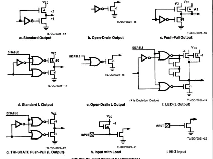
COP420/421 outputs have the following optional configura-tions, illustrated in Figure 9a:
a. Standard-an enhancement mode device to ground in conjunction with a depletion-mode device to Vee, com-patible with TIL and CMOS input requirements. Avail-able on SO, SK, and all D and G outputs.
b. Open-Draln-an enhancement-mode device to ground only, allowing external pull-up as required by the user's application. Available on SO, SK, and all D and G out-puts.
c. Push-Pull-An enhancement-mode device to ground in conjunction with a depletion-mode device paralleled by an enhancement-mode device to Vee. This configuration has been provided to allow for fast rise and fall times when driving capacitive loads. Available on SO and SK outputs only.
d. Standard L-same as a., but may be disabled. Available on L outputs only.
Functional Description COP420/COP421/COP422,
COP320/COP321/COP322
(Continued)f. LED Direct Drive-an enhancement-mode device to ground and to Vee, meeting the typical current sourcing requirements of the segments of an LED display. The sourcing device is clamped to limit current flow. These devices may be turned off under program control (See Functional Description, EN Register), placing the outputs in a high-impedance state to provide required LED seg· ment blanking for a multiplexed display.
g. TRI-STATE Push-Pull-an enhancement-mode device to ground and Vee. These outputs are TRI-STATE out-puts, allowing for connection of these outputs to a data bus shared by other bus drivers.
COP420/COP421 inputs have the following optional config-urations:
h. An on-chip depletion load device to Vee.
I. A Hi-Z input which must be driven to a "1" or "0" by external components.
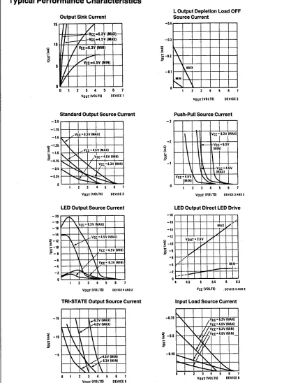
The above input and output configurations share common enhancement-mode and depletion-mode devices. Specifi-cally, all configurations use one or more of six devices (numbered 1-6, respectively). Minimum and maximum cur· rent (lOUT and VOUT) curves are given in Figure 9b for each
of these devices to allow the designer to effectively use these I/O configurations in designing a COP420/421 sys-tem.
The SO, SK outputs can be configured as shown in a., b., or c. The 0 and G outputs can be configured as shown in a. or
b. Note that when inputting data to the G ports, the G out-puts should be set to "1." The L outout-puts can be configured as in d.,
e.,
f. or g.An important point to remember if using configuration d. or f. with the L drivers is that even when the L drivers are disabled, the depletion load device will source a small amount of current (see Figure 9b, device 2); however, when the L lines are used as input, the disabled depletion device can
not
be relied on to source sufficient current to pull an input to logic" 1".COP421
If the COP420 is bonded as a 24-pin device, it becomes the COP421, illustrated in Figure 2, COP420/421 Connection Diagrams. Note that the COP421 does not contain the four general purpose IN inputs (lN3-INo). Use of this option pre-cludes, of course, use of the IN options, interrupt feature, and the MICROBUS option which uses IN1-IN3. All other options are available for the COP421.
TLlDD/6921-15
TL/DD/6921-14
a. Standard Output b. Open-Oraln Output
TLlDD/6921-16
c. Push-Pull Output
TL/DD/6921-17
d. Standard L Output
TL/DD/6921-20
g. TRI-STATE Push-Pull (L Output)
D"ABlE~~
•TL/DD/6921-18
(& is Depletion Device) TL/DD/6921-19
e. Open-Drain L Output f. LED (L Output)
Vee
cmi
#6IN'~~f
TI,.IDD/6921-21
[image:12.486.27.443.276.586.2]h. Input with Load
FIGURE 9a. Input/Output Configurations
1·123
INPUT~~
TL/DD/6921-22
I. HI-Z Input
o
"'CI ~
I\)
o
...
o
o
"'CI ~
I\)
...
...
o
o
"'CI ~
I\) I\)
...
o
o
"'CI W
I\)
o
...
o
o
"'CI W
I\)
...
...
o
o
"'CI W
I\) I\)
N N
Cf)
Ill.
o
[image:13.486.42.459.42.590.2]o
...
,...
NCf)
Ill.
o
o
...
o
N
Cf)
Ill.
o
o
...
N N ~Ill.
o
o
...
,...
N ~
Ill.
o
o
...
o
N ~Ill.
o
o
Typical Performance Characteristics
C
.!
...
::>o
Output Sink Current
VOUT (VOL TSI DEVICE 1
Standard Output Source Current
- 2.0 r--r-,---,--.---r-,--,
-1.75 1--+-+--+-1--+-+--1
c-
I•25E
i;
-1.0 ~+!\d"":"';-'1"---;--'--r-'--t--t!E -0.75 ~~--I~+,L--!--+--t--t - 0.5 l:---P...,..r--fi-~++-+-+--1
VOUl (VOL TSI DEVICE 2
LED Output Source Current
-20r-~-.-~-~~--r-' -18~~~+--+--+--4-+-1 -16~~~~~-~--t--r~
-14 "-:-+--~-+--+---I--+---t
C -12 I-~-f-::::,¥f--+--+--+---t
E
i;
-10 1-~-\-+-4r-+--+--+--1 E - 8 1-~-\+--+-\-*~--+--1-61--+-~~~~--I~~~
-4 I-~-~~-~--t--r--t
-2~~~~~~~-4-+-1
VOUT (VOL TSI DEVICE 4 AND Z
TRI-STATE Output Source Current
-15
C -10
.!
...
::>E
-5
VOUT (VOLTSI DEVICE 5
-0.4
-0.3
C
.!
~-0.2
-0.1
-18
-16
-14
-12
1-10
...
~ -8
-6
-4
-2
L Output Depletion Load OFF Source Current
1\
\
I\.MAX
MIN
\
~
'\
VOUT (VOL lSI DEVICE 2
Push-Pull Source Current
VOUT (VOL lSI DEVICE 3 AND Z
LED Output Direct LED Drive
MAX
/ '
..,V VOur- 2.GV , //~
, /
",
"
~t~~
-...
~-o
4 4.5 5.5 6.5
Vcc (VOLTSI . DEVICE 4 AND Z
Input Load Source Current
1-0.5 J---31cl---t~Wh·, !;
E
FIGURE 9b. COP420/COP421 Input/Output Characteristics 1-124
Typical Performance Characteristics
(Continued)!
...
§
10
2 3 4
VoUT (VOLTS) DEVICE 1
Standard Output Source Current
-1.75 r----r-,--.---r-,--.--..
!
-1.0 1--''rII'-T-t----t--t--t--+-l...
§
-0.75 1---+-"'<---+-'1.--+----+--+--+---1!
...
§
-0.53 4
VOUT (VOLTS) DEVICE 2
LED Output Source Current
-24~_T-~-~_T-~~
3. 4
VOUT (VOLTS) DEVICE 4 AND 2
TRI·ST ATE Output Source Current
-15~-+-~-~_+-~-t--;
-10
-5
4
VoUT (VOLTS) DEVICE 5
L Output Depletion Load OFF Source Current
1-
0.4~ -0.3
~+
-0.2 -0.1
~_I\
2 3 4 5 VOUT (VOLTS) DEVICE 2
Push· Pull Source Current
- 3.0 r---...-TT"""""T"I'""'"I""'T"-.----,
- 2.5 I---+\---t--+~"'+'=-+-___l - 2.0 f--+-+--tt--H-t-1
j
;: -1.5 1---+--+~..._4+--.r.++--+--___l
§
2 4
YOUT (VOLTS) DEVICE 2 AND 3
LED Output Direct LED Drive
.
-14
-12
/
/MAX -10; (
!.
...
-8§
-6/
"
.1.
,
VoUT = 2.0V,
,
-4
,
-2
.-~
".,-...
-o
4.0 4.5 S.D 5.5 6.0
VCC (VOLTS) DEVICE 4 AND 2
Input Load Source Current
-1.0 f--+-~-t--+-+----l
- 0.2 I--'---\~-~--"'k---x:__-+----l
4
[image:14.489.33.440.39.595.2]VoUT (VOLTS) 5 DEVICE 6
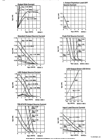
FIGURE 9c. COP320/COP321 Input/Output Characteristics
1·125
TL/DD/6921-24
o
"0 ~ No
...
o
o
"0 ~ N
...
...o
o
"0 ~ N N
...
o
o
"0 W N
o
...
o
o
"0 W N
...
...o
o
"0
W
N N
~ r---~ ~
CW')
a.
o
o
...
...
~
CW')
a.
o
o
...
o
~
CW')
a.
o
o
...
~ ~ ~a.
8
...
...
~ ~a.
o
o
...
o
~ ~a.
o
o
Instruction Set
Table I is a symbol table providing internal architecture, struction operand and operational symbols used in the in-struction set table.
Table " provides the mnemonic, operand, machine code, data flow, skip conditions and description associated with each instruction in the COP420/COP421/COP422 instruc-tion set.
TABLE I. COP420/421/422/320/321/322 Instruction Set Table Symbols
Symbol Definition INTERNAL ARCHITECTURE SYMBOLS A 4-bit Accumulator
8 6-bit RAM Address Register 8r Upper 2 bits of 8 (register address) Bd Lower 4 bits of 8 (digit address) C 1-bit Carry Register
D 4-bit Data Output Port EN 4-bit Enable Register
G 4-bit Register to latch data for G 1/0 Port IL Two 1-bit latches associated with the IN3 or
INo inputs IN 4-bit Input Port L S-bit TRI-STATE 1/0 Port
M 4-bit contents of RAM Memory pointed to by 8 Register
PC 9-bit ROM Address Register (program counter)
Q S-bit Register to latch data for L 1/0 Port SA 1 O-bit Subroutine Save Register A S8 1 O-bit Subroutine Save Register 8 SC 10 Subroutine Save Register A SIO 4-bit Shift Register and Counter SK Logic-Controlled Clock Output
Symbol Definition INSTRUCTION OPERAND SYMBOLS
d 4-bit Operand Field, 0-15 binary (RAM Digit Select) r 2-bit Operand Field, 0-3 binary (RAM Register
Select)
a 10-bit Operand Field, 0-1023 binary (ROM Address) y 4-bit Operand Field, 0-15 binary (Immediate Data) RAM(s) Contents of RAM location addressed by s ROM(t) Contents of ROM location addressed by t
OPERATIONAL SYMBOLS
+
Plus-
Minus...
Replaces~ Is exchanged with
= Is equal to
A
The one's complement of AE9 Exclusive-OR
: Range of values
TABLE II. COP420/421 1422/320/321 1322 Instruction Set
Hex Machine Mnemonic Operand
Code Language Code Data Flow Skip Conditions Description (Binary)
ARITHMETIC INSTRUCTIONS
ASC 30 10011100001 A
+
C+
RAM(8) ... A Carry Add with Carry, Skip on Carry ... C CarryADD 31 1001110001
I
A+
RAM(8) ... A None Add RAMtoA ADT 4A 1010011010I
A+
1010 ... A None Add Ten toA AISC y 5- 10101I
yI
A+
y ... A Carry Add immediate, Skip onCarry (y #-0)
CASC 10 10001100001
A
+
RAM(8)+
C ... A Carry Complement and Add with Carry ... C Carry, Skip on Carry CLRA 00 10000100001 0"'" A None Clear ACOMP 40 10100100001
A"'"
A None One's complement of A to ANOP 44 10100101001 None None No Operation
RC 32 10011100101 "0" ... C None ResetC SC 22 10010100101 "1" ... C None SetC
XOR 02 10000100101 A E9 RAM(8) ... A None Exclusive-OR RAM with A
Instruction Set
(Continued)TABLE II. COP420/421/422/320/321/322 Instruction Set (Continued)
Hex Machine Mnemonic Operand
Code Language Code Data Flow Skip Conditions (Binary)
TRANSFER OF CONTROL INSTRUCTIONS
JID FF 1111111111
I
ROM (PCs, A,M) ---+ None PC7:0JMP a 6- 1011O lOOlaai a ---+ PC None
-
-
I
a7:0I
JP a
-
-
11I
a6:0I
a ---+ PC6:0 None (pages 2,3 only)or
- -
111I
as:oI
a ---+ PCs:o (all other pages)JSRP a
-
-
110 1 as:oI
PC+
1 ---+ SA ---+ SB ---+ SC None 010 ---+ PCS:6a ---+ PCs:o
JSR a 6- 10110110
I
a9:sl PC+
1 ---+ SA ---+ SB ---+ SC None- -
I
a7:0I
a ---+ PCRET 48 10100 11000
I
SC ---+ SB ---+ SA ---+ PC None RETSK 49 10100110011 SC ---+ SB ---+ SA ---+ PC Always Skipon Return MEMORY REFERENCE INSTRUCTIONS
CAMO 33 10011100111 A ---+ 07:4 None 3C 10011111001 RAM (B) ---+ 03:0
COMA 33 10011100111 07:4 ---+ RAM (B) None 2C 10010 11100
I
03:0 ---+ ALD r -5 100lrl01011 RAM(B) ---+ A None Br Ell r ---+ Br
LDD r,d 23 10010100111 RAM(r,d) ---+ A None
--
1001 rI
d 1LOID . BF 11011 11111 1 ROM(PCg:a.A.M) ---+ 0 None SB ---+ SC
RMB 0 4C 10100111001
o
---+ RAM(B)o None 1 45 10100101011o
---+ RAM(B)12 42 10100100101
o
---+ RAM(B)2 3 43 10100100111o
---+ RAM(Bb5MB 0 4D 1010011101 1 1 ---+ RAM(B)o None 1 47 10100111011 1 ---+ RAM(Bh
2 46 10100101101 1 ---+ RAM(B)2 3 4B 1010011011 1 1 ---+ RAM(Bb
STII Y 7- 10111 1 y 1 y ---+ RAM (B) None Bd
+
1 ---+ BdX r -6 100
I
rI
0110 1 RAM (B) ~ A None Br Ell r ---+ BrXAD r,d 23 10010100111 RAM(r,d) ~ A None
- -
110I
rI
d 11-127
Description
Jump Indirect (Note 3)
Jump
Jump within Page (Note 4)
Jump to Subroutine Page (Note 5)
Jump to Subroutine
Return from Subroutine Return from Subroutine then Skip
Copy A, RAM to 0
Copy 0 to RAM, A
Load RAM into A Exclusive-OR Br with r
Load A with RAM pointed to directly by r,d
Load 0 Indirect (Note 3)
Reset RAM Bit
Set RAM Bit
Store Memory Immediate and Increment Bd
Exchange RAM with A, Exclusive-OR Br with r
Exchange A with RAM pointed to directly by r,d
o
"tJ
~
I\)
o
...
o
o
"tJ
~
I\)
...
...
o
o
"tJ
~
I\) I\)
...
o
o
"tJ
W I\)
o
...
o
o
"tJ
W I\)
...
...
o
o
"tJ
W I\) I\)
C'I C'I
C")
a.
[image:17.487.38.458.37.597.2]o
o
...
....
C'IC")
a.
o
o
...
QC'I
C")
a.
o
o
...
C'I C'I
'11:1'
D-O
o
...
....
C'I
'11:1'
a.
o
o
...
Q
C'I
'11:1'
a.
o
o
Instruction Set
(Continued)TABLE II. COP420/421 1422/320/3211322 Instruction Set (Continued)
Hex Machine
Mnemonic Operand
Code Language Code DataFlow Skip Conditions
(Binary) MEMORY REFERENCE INSTRUCTIONS (Continued)
XDS r -7 1 00 1 r 1 0111 I RAM (B) +-+ A Bd decrements past 0
Bd -1 -+ Bd Br (!) r -+ Br
XIS r -4 100 I r I 0100 I RAM(B) +-+ A Bd increments past 15
Bd
+
1 -+ Bd Br (!) r -+ BrREGISTER REFERENCE INSTRUCTIONS
CAB 50 10101100001 A -+ Bd None
CBA 4E 10100111101 Bd -+ A None
LBI r,d
-
-
100Irl(d-1)1 r,d -+ B Skip until not a LBI(d
=
0,9:15) or 33 1001110011 I--
110 I r I d I(any d)
LEI y 33 1001110011 I y -+ EN None
6- 10010 1
Y.. I
XABR 12 10001100101 A +-+ Br (0,0 -+ A3.A2) None TEST INSTRUCTIONS
SKC 20 10010100001 C
=
"1"SKE 21 1001010001 I A
=
RAM (B)SKGZ 33 1001110011 I G3:0
=
021 1001010001 I
SKGBZ 33 1001110011 I 1st byte
0 01 1000010001 I
} 2nd byte
Go
=
01 11 1000110001 I G1
=
02 03 1000010011 I G2
=
03 13 1001010011 I G3
=
0SKMBZ 0 01 10000100011 RAM(B)o
=
01 11 1000110001 I RAM(Bh
=
02 03 1000010011 I RAM(B)2
=
03 13 10001100111 RAM(Bb
=
0SKT 41 10100100011 A time-base counter
carry has occurred since last test
1-128
Description
Exchange RAM with A and Decrement Bd, Exclusive-OR Br with r Exchange RAM with A and Increment Bd, Exclusive·OR Br with r
Copy A to Bd Copy BdtoA Load B Immediate with r,d (Note 6)
Load EN Immediate (Note 7)
Exchange A with Br
Skip if C is True Skip if A Equals RAM Skip if G is Zero (all 4 bits) Skip if G Bit is Zero
Skip if RAM Bit is Zero
Instruction Set
(Continued)TABLE II. COP420/421/422/320/321/322 Instruction Set (Continued) Machine
Hex Mnemonic Operand
Code Language Code Data Flow Skip Conditions Description (Binary)
INPUT IOUTPUT INSTRUCTIONS
ING 33 10011100111 G~A None Input G Ports to A 2A 10010 11010 1
ININ 33 10011100111 IN ~ A None Input IN Inputs to A (Note 2) 28 10010 11000 1
INIL 33 10011100111 IL3, CKO, "0", ILo ~ A None Input IL Latches to A
29 10010 110011 (Note 3)
INL 33 10011100111 L7:4 ~ RAM (B) None Input L Ports to RAM, A 2E 10010111101 L3:0 ~ A
OBD 33 10011100111 Bd ~ D None Output Bd to D Outputs 3E 10011 11110 1
OGI Y 33 10011100111 y~G None Output to G Ports Immediate
5- 10101 1 y 1
OMG 33 10011100111 RAM(B) ~ G None Output RAM to G Ports 3A 10011 11010 1
XAS 4F 1010011111 1 A ~ SIO,C ~ SKL None Exchange A with SIO (Note 3)
Note 1: All subscripts for alphabetical symbols indicate bit numbers unless explicitly defined (e.g., Br and Bd are explicitly defined). Bits are numbered 0 to N where
o
signifies the least significant bit (low-order, right-most bit). For example, A3 indicates the most significant (left-most) bit of the 4-bit register. Note 2: The ININ Instruction is not available on the COP421/COP321 and COP422/COP322 since these devices do not contain the IN inputs. Note 3: For additional information on the operation of the XAS, JID, LQID, INIL, and SKT instructions, see below.Note 4: The JP instruction allows a jump, while in subroutine pages 2 or 3, to any ROM location within the two-page boundary of pages 2 or 3. The JP instruction, otherwise, permits a jump to a ROM location within the current 64-word page. JP may not jump to the last word of a page.
Note 5: A JSRP transfers program control to subroutine page 2 (0010 is loaded into the upper 4 bits of Pl. A JSRP may not be used when in pages 2 or 3. JSRP may not jump to the last word in page 2.
Note 6: LBI is a single-byte instruction if d = 0, 9, 10, 11, 12, 13, 14, or 15. The machine code for the lower 4 bits equals the binary value of the "d" data minus 1,
e.g., to load the lower four bits of B (Bd) with the value 9 (10012), the lower 4 bits of the LBI instruction equal B (10002)' To load 0, the lower 4 bits of the LBI instruction should equal 15 (11112)'
Note 7: Machine code for operand field y for LEI instruction should equal the binary value to be latched into EN, where a "1" or "0" in each bit of EN corresponds with the selection or deselection of a particular function associated with each bit. (See Functional Description, EN Register.)
Description of Selected Instructions
The following information is provided to assist the user in understanding the operation of several unique instructions and to provide notes useful to programmers in writing
COP420/421 programs.
XAS INSTRUCTION
XAS (Exchange A with SIO) exchanges the 4-bit contents of the accumulator with the 4-bit contents of the SIO register. The contents of SIO will contain serial-in/serial-out shift reg-ister or binary counter data, depending on the value of the EN register. An XAS instruction will also affect the SK out-put. (See Functional Description, EN Register, above.) If
1-129
SIO is selected as a shift register, an XAS instruction must be performed once every 4 instruction cycles to effect a continuous data stream.
JID INSTRUCTION
JID (Jump Indirect) is an indirect addressing instruction, transferring program control to a new ROM location pointed to indirectly by A and M. It loads the lower 8 bits of the ROM address register PC with the
contents
of ROM addressed by the 10-bit word, PC9:B, A, M. PCg and PCB are not affected by this instruction.Note that JID requires 2 instruction cycles to execute.
0
""C ~ N 0
...
0
0
""C ~ N ...A.
...
0
0
""C ~ N N
...
0
0
""C
w
N 0...
0
0
""C
w
N ...A....
0
0
""C
w
N NN N
CW)
Q.
o
o
"-
--NCW)
Q.
o
o
"-
o
N
CW)
Q.
o
o
"-N
N ~ Q.
o
o
"-
--N ~ Q.o
o
"-
o
N ~ Q.
o
o
Description of Selected Instructions
(Continued)INIL INSTRUCTION
INIL (Input IL Latches to A) inputs 2 latches, IL3 and ILa (see
Figure 1tJ) and CKO into A. The IL3 and ILa latches are set if
a low-going pulse ("1" to "0") has occurred on the IN3 and INo inputs since the last INIL instruction, provided the input pulse stays low for at least two instruction times. Execution of an INIL inputs IL3 and ILa into A3 and AO respectively, and resets these latches to allow them to respond to subse-quent low-going pulses on the IN3 and INo lines. If CKO is
~ask programmed as a general purpose input, an INIL will Input the state of CKO into A2. If CKO has not been so programmed, a "1" will be placed in A2. A "0" is always placed in A1 upon the execution of an INIL. The general purpose inputs IN3-INo are input to A upon execution of an ININ instruction. (See Table II, ININ instruction.) INIL is use-ful in recognizing pulses of short duration or pulses which occur too often to be read conveniently by an ININ instruc-tion.
Note: IL latches are not cleared on reset.
COP420
[image:19.486.49.241.149.343.2]TLlDD/6921-25
FIGURE 10
LQID INSTRUCTION
LaiD (Load a Indirect) loads the 8-bit a register with the contents of ROM pointed to by the 1 O-bit word PCg. PCe. A, M. LaiD can be used for table lookup or code conversion such as 8CD to seven-segment. The LaiD instruction "pushes" the stack (PC
+
1 ----+ SA ----+ S8 ----+ SC) and replaces the least significant 8 bits of PC as follows: A ----+ PC7:4, RAM(8) ----+ PC3:0, leaving PCg and PCe un-changed. The ROM data pointed to by the new address is fetched and loaded into the a latches. Next, the stack is "popped" (SC ----+ S8 ----+ SA ----+ PC), restoring the saved value of PC to continue sequential programexecu-1-130
tion. Since LaiD pushes S8 ----+ SC, the previous contents of SC are lost. Also, when LaiD pops the stack, the previ-ously pushed contents of S8 are left in SC. The net result is that the content of S8 are placed in SC (S8 ----+ SC). Note that LaiD takes two instruction cycle times to execute.
SKT INSTRUCTION
The SKT (Skip On Timer) instruction tests the state of an internal 10-bit time-base counter. This counter divides the instruction cycle clock frequency by 1024 and provides a latched indication of counter overflow. The SKT instruction tests this latch, executing the next program instruction if the latch is not set. If the latch has been set since the previous test, the next program instruction is skipped and the latch is reset. The features associated with this instruction, there-fore, allow the COP420/421 to generate its own time-base for real-time processing rather than relying on an external input signal.
For example, using a 2.097 MHz crystal as the time-base to the clock generator, the instruction cycle clock frequency will be 131 kHz (crystal frequency + 16) and the binary counter output pulse frequency will be 128 Hz. For time-of-day or similar real-time processing, the SKT instruction can call a routine which increments a "seconds" counter every 128 ticks.
INSTRUCTION SET NOTES
a. The first word of a COP420/421 program (ROM address 0) must be a CLRA (Clear A) instruction.
b. Although skipped instruction are not executed, one in-struction cycle time is devoted to skipping each byte of the skipped instruction. Thus all program paths take the same number of cycle times whether instructions are skipped or executed except JID and LaiD. LaiD and JID take two cycle times if executed and one if skipped. c. The ROM is organized into 16 pages of 64 words each.
Option List
The COP420/421 1422 mask-programmable options are
as-signed numbers which correspond with the COP420 pins. The following is a list of COP420 options. When specifying a COP421 or COP422 chip, Options 9, 10, 19, 20 and 29 must all be set to zero. When specifying a COP422 chip, Options 21, 22, 27 and 28 must also be zero, and Option 2 must not be a 1. The options are programmed at the same time as the ROM pattern to provide the user with the hardware flexi-bility to interlace to various 1/0 components using little or no external circuitry.
Option 1 = 0: Ground-no options available Option 2: CKO Pin
= 0: clock generator output to crystal
o
not available if option 3 = 4 or 5)= 1: Pin is RAM power supply (VR) input (Not available on COP422/COP322)
= 2: general purpose input with load device
= 4: general purpose Hi Z input Option 3: CKI Input
= 0: crystal input devided by 16
= 1: crystal input divided by 8
= 2: TTL external clock input divided by 16
= 3: TTL external clock input divided by 8
= 4: single-pin RC controlled oscillator (+ 4)
= 5: Schmitt trigger clock input (+ 4) Option 4: RESET Pin
= 0: load devices to Vee
= 1: Hi-Z input Option 5: L7 Driver
= 0: Standard output (Figure 90) = 1: Open-Drain output (E)
= 2: LED direct drive output (F)
= 3: TRI-STATE push-pull output (G) Option 6:
La
Driversame as Option 5 Option 7: L5 Driver
same as Option 5 Option 8:
4
Driversame as Option 5 Option 9: IN1 Input
= 0: load devices to Vee (H)
= 1: Hi-Z input (I) Option 10: IN2 Input same as Option 9
Option 11 = 0: Vee Pin-no options available Option 12: L3 Driver
same as Option 5 Option 13: L2 Driver same as Option 5 Option 14: L1 Driver same as Option 5 Option 15:
Lo
Driver same as Option 51-131
Option 16: SI Input same as Option 9 Option 17: SO Driver
= 0: standard output (A)
= 1: open-drain output (B)
= 2: push-pull output (C) Option 18: SK Driver
same as Option 17 Option 19: INo Input
same as Option 9 Option 20: IN3 Input same as Option 9 Option 21: Go 1/0 Port
= 0: Standard output (A)
= 1: Open-Drain output (B) Option 22: G1 1/0 Port
same as Option 21 Option 23: G2 1/0 Port
same as Option 21 Option 24: G3 1/0 Port
same as Option 21 Option 25: 03 Output
= 0: Standard output (A)
= 1: Open-Drain output (8) Option 26: 02 Output
same as Option 25 Option 27: 01 Output same as Option 25 Option 28: Do Output same as Option 25 Option 29: COP Function
= 0: normal operation
= 1: MICROBUS option Option 30: COP Bonding
= 0: COP420 (28-pin device)
= 1: COP421 (24-pin device)
= 2: 28- and 24-pin device
= 3: COP422 (20-pin device)
=
4: 28- and 20-pin device= 5: 24- and 20-pin device
= 6: 28-, 24- and 20-pin device Option 31: In Input Levels
= 0: normal input levels
=
1: Higher voltage input levels ("0"=
1.2V, "1"=
3.6V) Option 32: G Input Levelssame as Option 31 Option 33: L Input Levels
same as Option 31 Option 34: CKO Input Levels
same as Option 31 Option 35: SI Input Levels
same as Option 31
o
"'0
~
I\)
o
...
o
o
"'0
~
I\)
...
...o
o
"'0
~
I\) I\)
...
o
o
"'0W
I\)
o
...o
o
"'0W
I\)
...
...o
o
"'0
W
N N
C")
Q.
o
[image:21.487.50.239.43.545.2]o
...
..-N
C")
Q.
o
o
...
o
N
C")
Q.
o
o
...
N N -.::t Q.
o
o
...
..-N -.::t Q.o
o
...
o
N -.::t Q.
o
o
Option List
(Continued) COP OPTION LISTThe following option information is to be sent to National along with the EPROM.
OPTION DATA
OPTION 1 VALUE - 0 IS: GROUND PIN OPTION 2 VALUE - _ _ _ _ IS: CKO PIN OPTION
OPTION OPTION OPTION OPTION OPTION OPTION
3 4 VALUE-5 VALUE =
6 VALUE =
7 VALUE =
8 VALUE =
9 VALUE =
_ _ _ _ IS: CKIINPUT _ _ _ _ IS: RESET INPUT _ _ _ _ IS: L7 DRIVER _ _ _ _ IS: L6 DRIVER _ _ _ _ IS: Ls DRIVER _ _ _ _ IS: L4 DRIVER _ _ _ _ IS: IN1 INPUT OPTION 10 VALUE = _ _ _ _ IS: IN21NPUT OPTION 11 VALUE - _ _ _ _ IS: VCC PIN OPTION 12 VALUE - _ _ _ _ IS: L3 DRIVER OPTION 13 VALUE - _ _ _ _ IS: L2 DRIVER OPTION 14 VALUE - IS: L1 DRIVER OPTION 15 VALUE - _ _ _ _ IS: Lo DRIVER OPTION 16 VALUE - _ _ _ _ IS: SIINPUT OPTION 17 VALUE - _ _ _ _ IS: SO DRIVER OPTION 18 VALUE = _ _ _ _ IS: SK DRIVER OPTION 19 VALUE - _ _ _ _ IS: INo INPUT OPTION 20 VALUE - IS: IN3 INPUT OPTION 21 VALUE - _ _ _ _ IS: Go 1/0 PORT OPTION 22 VALUE - _ _ _ _ IS: G1 1/0 PORT OPTION 23 VALUE - _ _ _ _ IS: G21/0 PORT OPTION 24 VALUE - _ _ _ _ IS: G31/0 PORT OPTION 25 VALUE - _ _ _ _ IS: D3 OUTPUT OPTION 26 VALUE - IS: D2 OUTPUT OPTION 27 VALUE - _ _ _ _ IS: D1 OUTPUT OPTION 28 VALUE - _ _ _ _ IS: Do OUTPUT OPTION 29 VALUE - _ _ _ _ IS: COP FUNCTION OPTION 30 VALUE - _ _ _ _ IS: COP BONDING OPTION 31 VALUE - _ _ _ _ IS: IN INPUT LEVELS OPTION 32 VALUE - IS: G INPUT LEVELS OPTION 33 VALUE - _ _ _ _ IS: L INPUT LEVELS OPTION 34 VALUE - _ _ _ _ IS: CKO INPUT LEVELS OPTION 35 VALUE - _ _ _ _ IS: SIINPUT LEVELS TEST MODE (Non-Standard Operation)
The SO output has been configured to provide for standard test procedures for the custom-programmed COP420. With SO forced to logic "1", two test modes are provided, de-pending upon the value of SI:
a. RAM and Internal Logic Test Mode (SI = 1) b. ROM Test Mode (SI = 0)
These special test modes should not be employed by the user; they are intended for manufacturing test only. APPLICATION # 1: COP420 General Controller
Figure 8 shows an interconnect diagram for a COP420 used
as a general controller. Operation of the system is as fol-lows:
1. The LrLo outputs are configured as LED Direct Drive outputs, allowing direct connection to the segments of the display.
1-132
2. The D3-DO outputs drive the digits of the mulitplexed dis-play directly and scan the columns of the 4 x 4 keyboard matrix.
3. The IN3-INo inputs are used to input the 4 rows of the keyboard matrix. Reading the IN lines in conjunction with the current value of the D outputs allows detection, de-bouncing, and decoding of anyone of the 16 keyswitch-es.
4. CKI is configured as a single-pin oscillator input allowing system timing to be controlled by a single-pin RC net-work. CKO is therefore available for use as a VR RAM power supply pin. RAM data integrity is thereby assured when the main power supply is shut down (see RAM Keep-Alive option description).
5. SI is selected as the input to a binary counter input. With SIO used as a binary counter, SO and SK can be used as general purpose outputs.
6. The 4 bidirectional G I/O ports (G3-GO) are available for use as required by the user's application.
APPLICATION #2: MUSICAL ORGAN AND MUSIC BOX Play Mode: Twenty-five musical keys and 25 LEDs are pro-vided to denote F to F with half notes in between. All the keys and LEDs are directly detected and driven by the mi-croprocessor. Depression of the key will give the corre-sponding musical note and light up the correcorre-sponding LED. Clear: Memory is provided to store a played tune. Depres-sion of the CLEAR key erases the memory and the micro-processor is ready to store new musical notes. A maximum of 28 notes can be stored where each note can be of one to eight musical beats. (Two bytes of memory are required to store one musical note. Any note longer than eight musical beats will require additional memory space for storage.) Playback: Depression of this button will playback the tune stored in the memory since last "clear."
Preprogrammed Tunes: There are ten preprogrammed tunes (each has an average of 55 notes) masked in the chip. Any tune can be recalled by depressing the "Tune Button" followed by the corresponding "Sharp Key." Learn Mode: This mode is for the player to learn the ten preprogrammed tunes. By pressing the "Learn Button" fol-lowed by the corresponding "Sharp Key," the LEDs will be lighted up one by one to indicate the notes of the selected tune. The LED will remain "on" until the player presses the correct musical key; the LED for the next note will then be lighted up.
Pause: In addition to the 25 musical keys, there is a special pause key. The depression of this key generates