© 2017, IRJET | Impact Factor value: 5.181 | ISO 9001:2008 Certified Journal | Page 582
Designing of Adders and Vedic Multiplier using Gate Diffusion Input
Kota Rashmi Reddy
1, D. Praveen Kumar
21
M.tech Student, Mallareddy College of Engineering(MREC), Telangana, India
2Associate Professor, Mallareddy College of Engineering (MREC), Telangana, India
---***---
Abstract -
Advancement in the VLSI technology leads tothe reduction in chip size and increase in chip density. As the chip density increases the overall power consumption and the complexity also increases. As the performance of any system is measured mainly on power consumption, it is recommended to use low power VLSI Design techniques. In this paper, we would discuss the GDI logic and its application in the modeling of adders for Vedic Multiplier design. Adders are of prime importance, the design of reliable and efficient adder for a VLSI based embedded application matters. This paper primarily deals with the design of Ripple Carry Adder, Kogge Stone Adder, and Brent Kung Adder using CMOS and GDI logic. Urdhava Triyagbhayam sutra is used to design multipliers. Later a comparative analysis based on the simulation results is made.
Key Words:
Gate diffusion Input, Ripple Carry Adder
(RCA), Kogge Stone Adder (KSA), Brunt Kung Adder (BKA), 4X4 Vedic Multiplier number of transistors, Power, an Delay.
1. INTRODUCTION
The increasing prominence of portable systems demands high chip density along with low power consumption. Now a day’s reducing the power consumption has become an important goal in the design of digital integrated circuits. One of the methods to meet this goal is the design improvements at the logic level. Traditional digital circuits were designed using complementary metal oxide semiconductors (CMOS). A new Low power VLSI design technique called GDI (Gate diffusion Input) is used in the design of digital components. This Technique has comparatively more advantages over the traditional CMOS design. This paper gives comparative analysis based on the performance of CMOS and GDI techniques.
A Multiplier is the fundamental block of almost all the processors. Hence a high-speed and area efficient multiplier is needed. Multiplication operation is performed by the series or parallel addition concepts. Design of adders with GDI technique will improve the performance of multipliers.
2. GDI LOGIC
Gate Diffusion Input (GDI) logic is a low power Very Large Scale Integrated (VLSI) design technique which was introduced as an alternative to CMOS logic design. This
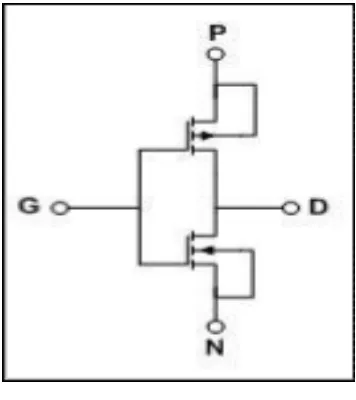
technique is a two transistor implementation of complex logic functions; Logic functions can be designed with fewer gates. GDI provides in cell swing restoration when operated in certain conditions and use of restoration buffers. Digital circuits designed using GDI logic will have less power consumption occupy a minimum area, gate count and delay in the circuit is reduced. Because of fewer gates, there is less design complexity.GDI cell is as shown in the below figure 2.1
[image:1.595.358.536.448.648.2]GDI cell looks similar to the CMOS inverter but the major difference is that the GDI cell has one PMOS and NMOS transistors connected in cascade resulting in three input terminals N, P, G. where N is the input terminal of NMOS, P is input to the PMOS and G is connected to the common gate of NMOS and PMOS. These terminals could be given a supply VDD or Grounded or input signal depending on the circuit design. In conventional CMOS inverter circuit, the PMOS and NMOS diffusion inputs are always either VDD or Ground
Figure 2.1 GDI CELL
© 2017, IRJET | Impact Factor value: 5.181 | ISO 9001:2008 Certified Journal | Page 583
Table 2.1 Logic Funtions of GDI Cell
3. DESIGN OF ADDERS
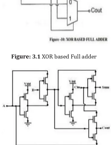
3.1 Full Adder
[image:2.595.334.554.343.490.2]A Full adder performs the addition operation on three-bit binary numbers A, B and C. The output of the full adder is SUM and Carry. It can be implemented using Two XOR gates and One MUX which is designed using GDI technique as shown in the below Figure-3.1
Figure: 3.1 XOR based Full adder
Figure 3.2 full adder design using GDI cell
The number of transistors used to design a full adder using GDI technique is 10, the area occupied by the full adder is 251.5-micrometer square and the power consumed is arround11.943µW. Whereas the full adder designed using
the conventional CMOS logic would occupy 634.48 µm
square area, 28 transistor and power consumption is 23.049µW. Comparative analysis between the gate count, area and power parameters between CMOS and GDI based adder illustrate the advantage of GDI logic in Low power VLSI design.
3.2 Ripple Carry Adder
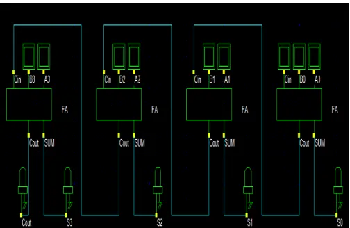
[image:2.595.75.250.396.507.2]Addition of N bit numbers is performed with the help of N full adders arranged such that the carry output of the full adder is input to the next full adder. This kind of arrangement is called Ripple carry adder. In Ripple Carry Adder the carry is rippled from the one adder to the next full adder. Ripple carry adder is simple to design and takes less time. However, the Ripple carry adder is relatively slow since each full adder must wait for the carry bit from the previous adders. Ripple carry adder is as shown in Figure 3.3
Figure 3.3 Ripple Carry Adder
Ripple carry adder is designed using four full adders which are designed using GDI logic. The gate count of the Ripple carry adders using GDI logic is 40 Transistors and the area is 804.19 µm square which is comparatively very less. The power consumed by the 4 bit RCA is 11.622µW.
3.3 Parallel Prefix Adders
[image:2.595.76.259.440.678.2]© 2017, IRJET | Impact Factor value: 5.181 | ISO 9001:2008 Certified Journal | Page 584
4 bit CLA Carry Equation is given as
C4 = (g4, p4) ο [ (g3, p3) ο [(g2, p2) ο (g1, p1)] ] (1) 4 bit PPA carry equation is given as
C4 = [(g4, p4) ο (g3, p3)] ο [(g2, p2 ) ο (g1, p1)] (2)
From the equations (1) and (2) it is observed that the carry look Ahead adder takes three steps to generate the carry whereas PPA takes two steps to generate the carry.
Parallel Prefix Adders are designed using the following structure which involves three stages –Pre Computing, Prefix computation, and Final Computation.
Pre Computing;
In this step generate and propagate signals corresponding to each pair of bits in A and B are obtained. These signals are given by the logic equations below:
Pi = Ai XOR Bi (3) Gi = Ai AND Bi (4) Prefix Stage:
This step involves computation of carries corresponding to each bit. It uses group propagate and generate as intermediate signals as per the below equation
(g L, p L) o (g R, p R) = (g L + p L . g R , p L , p R) (5)
(BC) generates the ordered pair in equation (5), the gray cell (GC) generates only left signal.
G=Gi or ( Pi and Pj ) (6) P = Pi and Pj (7)
[image:3.595.331.569.293.522.2]Practically, the equations (6) and (7) can be expressed using a symbol “o “denoted by Brent and Kung. Its function is same as that of a black cell. Gray cell represents equation (6)
Figure 3.4 Black cell and Gray cell
Final Computation
It is the final step which involves computation of sum bits by the logic given below
Si = Pi XOR Ci-1 (8)
3.3.1 Kogge Stone Adders (KSA)
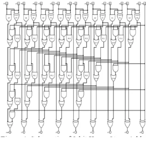
Kogge stone prefix adder is the fast adder because of its less delay and has the best performance in VLSI implementation. Kogge stone adder is used in wide number addition and it has the minimum fan out. Each vertical stage in KSA produces generate and propagate bits. In the last stage Generate bits are they are XORed with the initial propagate bits to produce the sum bits. 8-bit length Kogge Stone Adder designed using GDI logic is as shown in Figure 3.5.
[image:3.595.40.292.542.667.2]The transistor count of the Kogge stone adder designed using GDI logic is 190, the area is 10.08- millimeter square and the power consumed is 0.319mW.
Figure 3.5 8 bit KOGGE STONE ADDER
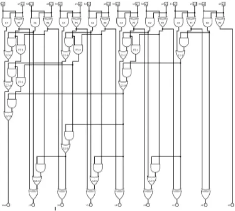
3.3.2 Brent Kung Adder (BKA)
Brent Kung Adder is a parallel prefix adder it has the minimum area, it is used for wide number addition. In BKA the fan-out is less at each stage. The design of 8 bit Brent Kung adder using GDI logic is as shown in figure 3.6.
© 2017, IRJET | Impact Factor value: 5.181 | ISO 9001:2008 Certified Journal | Page 585
Figure 3.6 8 Bit Brent Kung adder
4. VEDIC MULTIPLIERS
Multipliers are designed with the help GDI based adders and a Vedic multiplication technique called “Urdhva-Tiryakbhyam, Which can be used not only for decimal multiplication but also for binary multiplication. This mainly consists of the parallel generation of partial products and performing the addition operation simultaneously. This algorithm can be used for N×N bit multiplications. To illustrate this technique, let us consider two decimal numbers 252 and 846 and the multiplication of two decimal numbers 252×846 is explained by using the line diagram shown in below figure 6.
Figure 4.1 Multiplication of two decimal numbers
The architectures for 2×2, 4×4 bit modules are discussed in this section. Multiplication using Urdhva-Tiryakbhyam sutra is simple with less number of steps and also least computational time. The performance of the Vedic multiplier is further improved using GDI design technique.
4.1 Vedic Multiplier Block
This method can be explained with the help of two numbers with 2 bits each and the numbers are A and B where A=a0a1 and B=b0b1. The multiplication process can be explained by the following equations.
s0 = a0b0 (9)
c1s1 = a1b0 + a0b1 (10)
[image:4.595.326.556.336.491.2]c2 s2 = c1 + a1b1 (11) The final result is given as c2s2s1s0. A 2×2 Vedic multiplier block is implemented by using two half adders as shown in below Figure 4.1
Figure 4.1 Block Diagram of 2×2 Vedic Multiplier
4.2 4x4 Vedic Multiplier Block
In this section, we will discuss 4x4 bit Vedic multiplier. Let us consider two four bit numbers are A and B such that the individual bits are represented as the A3A2A1A0 and B3B2B1B0. The final output is C6S6S5S4S3S2S1S0. The partial products are calculated in parallel and hence delay is decreased enormously for the increase in the number of bits. The Least Significant Bit (LSB) S0 is obtained easily by multiplying the LSBs of the multiplier and the multiplicand. Here the multiplication is followed according to the figure 4.1. After performing all the steps the result (Sn) and Carry (Cn) is obtained and in the same way at each step the previous stage carry is forwarded to the next stage, and the process goes on.
S0 = A0B0 (12)
C1S1 = A1B0 + A0B1 (13)
[image:4.595.49.277.519.716.2]© 2017, IRJET | Impact Factor value: 5.181 | ISO 9001:2008 Certified Journal | Page 586
C3S3 = C2 + A0B3 + A3B0 + A1B2 + A2B1 (15) C4S4 = C3 + A1B3 + A3B1 + A2B2 (16)
C5S5 = C4 + A3B2 + A2B3 (17)
C6S6 = C5 + A3B3 (18)
[image:5.595.316.568.145.309.2]For clear understanding, observe the block diagrams for 4x4 as shown below figure 7, and within the block diagram 4x4 there are four 2x2 Vedic multiplier modules, and three RCAs which are of four-bit size are used. The four bit ripple carry adders are used for addition of two four bits, and likewise, totally four are used at intermediate stages 3 of the multiplier. The carry generated from the first ripple carry adder passed on to the next ripple carry adder and there are two zero inputs for second ripple carry adder. The arrangement of the RCAs is shown in below block diagram which can reduce the computational time such that the delay can be decreased.
Figure 4.2 Block Diagram of 4x4 Vedic Multiplier
The transistor count of the 4X4 Vedic Multiplier designed using GDI logic is 200; area is 6.446- millimeter square and the power consumed is 0.207mW
5. RESULTS AND DISCUSSIONS
The following are the simulation results and performance analysis of various adders. The design is done using CMOS and GDI logic using DSCH and Microwind 120nm technology. Part A shows schematic and simulation results for GDI logic based design and part B shows comparative analysis with performance measure as power, Delay, and Number of Transistor.
A. Simulation Results
[image:5.595.46.283.321.553.2]Ripple Carry Adder
[image:5.595.315.572.359.525.2]Figure 5.1 - 4 Bit Ripple carry Adder implemented using four Full Adders using GDI
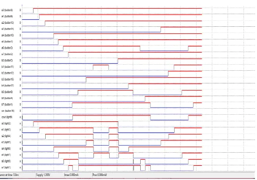
Figure 5.2 - Timing Diagram of Ripple carry Adder
[image:5.595.316.567.558.744.2]© 2017, IRJET | Impact Factor value: 5.181 | ISO 9001:2008 Certified Journal | Page 587 Kogge Stone Adder
[image:6.595.38.291.121.301.2]Figure 5.4 - 8 Bit Kogge Stone Adder using GDI
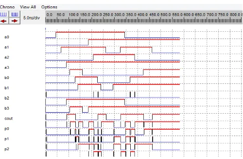
Figure 5.5 Timing Diagram of Kogge Stone Adder
Figure 5.6 Layout of Kogge Stone Adder
Brent Kung Adder
[image:6.595.317.570.333.511.2]Figure 5.7 8 Bit Brent Kung Adder using GDI
Figure 5.8 Timing Diagram of Brent Kung Adder
[image:6.595.38.281.333.526.2] [image:6.595.307.564.541.746.2] [image:6.595.49.564.544.747.2]© 2017, IRJET | Impact Factor value: 5.181 | ISO 9001:2008 Certified Journal | Page 588 4X4 Vedic Multiplier
Figure 5.10 Vedic Multiplier using GDI
[image:7.595.320.554.169.283.2]Figure 5.11 timing diagram of Vedic Multiplier
Figure 5.12 Lay out of Vedic Multiplier
B. Comparative Analysis
The comparative analysis of 4-bit ripple carry adder, 8 bit Brent Kung adder, 8-bit Kogge Stone Adder, and 4X4 Vedic multiplier implemented using the 2X2 multiplier, and RCA
is made regarding area and power. From the comparative analysis, it is clear that the GDI design gives a less power consumption and occupies less area compared to CMOS design style. The comparative analysis is as shown in the table below.
6. CONCLUSION
Adders are core and an essential block in many modules which involve computation and play a vital role in the design of multipliers. Hence the design and implementation of the adders are a prime concern. In this paper adders (RCA, KSA, BKA) based on GDI logic are used in Vedic Multiplier design. A comparative result is obtained. From the results, it is clear that the adders designed using GDI design style has less transistor count, occupy minimum area and power when compared to CMOS design style.
REFERENCES
[1] Mr. Kunjan D. Shinde, Mrs. Jayashree C. N. “Design of Fast and Efficient 1-bit Full Adder and its Performance Analysis”, Proceedings of the IEEE International Conference on “Control, Instrumentation, Communication and Computational Technologies (ICCICCT-2014)” at Noorul Islam University, Kumaracoil, Kanyakumari, Tamilnadu, India.
[2] IEEE TRANSACTIONS ON VERY LARGE SCALE INTEGRATION (VLSI) SYSTEMS, VOL. 10, NO. 5, OCTOBER 2002. Gate-Diffusion Input (GDI): A Power-EfficientMethod for Digital Combinatorial Circuits
[3] Review Of Various GDI Techniques For Low Power Digital Circuits International Journal of Emerging Technology and Advanced Engineering.
[4] AnasZainalAbidin, Syed Abdul Mutalid Al Junid, KhairulKhaiziMohdSharif, “A survey on 4 bit Brent kung PPA simulation study usingsilvaco EDA Tools”.
[image:7.595.38.288.309.472.2]