Properties of Broadband Non-Linear Lossy Materials
Employed in the Electromagnetic Inverse Scattering
during the Microchip Processing
Eytan Barouch1, Stephen L. Knodle1*, Steven A. Orszag2* 1Department of Mechanical Engineering, Boston University, Boston, USA
2Department of Mathematics, Yale University, New Haven, USA Email: [email protected]
Received May 20, 2013; revised June 20, 2013; accepted June 28, 2013
Copyright © 2013 Eytan Barouch et al. This is an open access article distributed under the Creative Commons Attribution License, which permits unrestricted use, distribution, and reproduction in any medium, provided the original work is properly cited.
ABSTRACT
A method has been designed and implemented to describe the optical properties of lossy materials as a continuous func- tions of a finite wave length spectrum, needed in analysis of the Maxwell-Material equations. Measurements of the in- dex of refraction (N) and the absorption coefficient (K) over a limited spectral range are used as input data. The (com- plex) permittivity function is then represented as a sum of five types of terms: a plasma term, a conductivity term, sev- eral Debye poles, several symmetric Lorentz poles as well as several asymmetric extended Lorentz (“XLorentz”) poles. All these terms are particular solutions of the Lifshitz integral equation describing the dispersion relation of a mono- chromatic electromagnetic wave. This representation facilitates the numerical solution of broadband direct and the in- verse scattering of electromagnetic waves for thin film stacks and composite physical structures, in particular those now employed by the microchip industry.
Keywords: Scattering; Inverse Scattering; Silicon-Material-Properties; Material Electric Permittivity
1. Introduction
The Maxwell-Material equations are given in its differ- ential form by:
D
ρ
(1a)
0
B
(1b)
E J
t
H (1c)
=
H E
t
(1d)
In Expressions (1a)-(1d), D, E, B, H represent the dis- placement and electric fields, the inductive and magnetic fields and J& are the current and charge density respectively.
With the continuing decrease in size and increase in density of nanodevices, including electronic microchips, there are increasing challenges in quality control and inspection and for improvements in manufacturing tech- nology. Gone are the days when scanning electron mi-
crographs (SEMs) could be routinely used in non-de- structive and non-invasive ways to inspect structures built as part of manufacturing processes. Now it is nec- essary to develop methods which are far less intrusive, can be used on-line during the nanoscale manufacturing itself. An attractive technique to address these issues is the use of broad-band electromagnetic wave scattering by nanostructures. On one hand, if the wavelength of the electromagnetic waves is substantially larger than the structural scales of the device then such radiation is likely to be non-destructive. Yet, if the scattering of these waves is (nearly) uniquely determined by the structures and vice versa then scattering results can be used as a diagnostic tool to discern geometric details.
The goal of this paper is to provide a framework in which to compute both the direct and the inverse scatter- ing of broad-band waves when propagating through complex lossy media. These computational methods and resulting simulations can then be used both to determine the scattering of waves by known structures (viz., direct scattering) and to infer the geometric structures and properties of devices known to produce a given (typically measured) spectrum (viz., inverse scattering). This is the
*Deceased. This work has been completed after the untimely departure
first of a series of two papers to describe this new com- putational methodology in detail.
In this first paper, the goal is to introduce powerful methods to characterize the optical properties of lossy materials, a critical first step in formulating the Maxwell equations for wave propagation in such media. In the second paper, the computational methodology for direct scattering is described and applied to a variety of nanos- tructures. An efficient solution of the inverse problem is also given. In this latter problem, the scattering data is given and used to infer the geometric structures that produce it.
The focus here is on materials employed by the mi- crochip industry, which include Si, SiO2, TiO2, Si3N4 etc.
It must be emphasized that the direct and quite simple approach of passing cubic-splines through the measured values of the actual material refractive index N and ab- sorption coefficient K is not effective since it lends itself to create wildly incorrect values outside the measurement domain. These incorrect values of N and K outside the measurement matrix have an overwhelming influence on both the direct and inverse scattering leading to quite poor results. The spurious results so produced are often a consequence of a pole in frequency space similar to the pole produced by perfectly absorbing layers (for the lat- ter, see [1]).
Traditionally, N for a given wavelength is expressed in terms of a principal-value integral of K over the entire spectrum and vice-versa. These equations are known as the Kramers-Kronig [3] relations and are derived from the analyticity of N + iK. Explicitly, the Kramers-Kronig relations are given as:
Tot N iK
= 1
π
K N P d
(2a)
= 1
π
N K P d
(2b) However, it is highly impractical to perform measure- ments over the entire spectrum, due to the limited capa-bility of measuring instruments at widely different wave- lengths. In practice a relatively narrow spectrum is mea- sured, necessitating simultaneous determinations of both the refractive and absorption indices. As such, the data so obtained is discrete in nature, rendering limited validity to broad band scattering, since the permittivity is ex- pressed as a continuous function in the Fourier trans- formed Maxwell-Material (MM) equations.The main numerical scheme employed in the current approach is based on a combination of the Powell and Brent methods for optimization (see [2]) in which the
assignment of the order of the parameters is correlated to their relative significance. Once one iteration is com- pleted on all parameters, a vector is created and a direc- tion of parameter movement is obtained. In this scheme, two controlling accuracy tolerances are employed to in- sure optimal results within a short computational time. The restriction on the ranges of the parameters imposed by physical principles, prohibits the use of a free-range optimization, and a standard map from infinite range to a finite domain is not practical. Therefore, the adopted method prevents the parameters to exit the allowed range by forcing the optimization scheme to rescale itself and stay within the physically acceptable domain. A particu- larly important restriction is that on the parameters of the plasma term. The plasma term can be easily decomposed into two partial fractions, one resembling a Debye pole and the other resembling a conductivity term. The term resembling a Debye term is subtracted from the conduc- tivity term, and if one has not restricted the plasma pa- rameters properly, one may end up with an unphysical negative conductivity.
Section 2 of this paper presents the basic material analysis of silicon and the approach to represent electri- cal properties of various materials employed in the inte- grated circuit (IC) industry. Section 3 discusses the re- sults of several other essential materials used in the IC industry which can be very different in nature from sili- con. For example, while PolySilicon is rather similar to crystalline silicon, it has quite different conductivity properties. In Paper II [3], numerical and computational considerations are discussed.
2. Material Analysis
The task of solving the Maxwell-Material equations is complicated by the fact that the displacement vector is proportional to the electric field, and the proportionaly function is a very complicated function of N and K. Since the equations are continuous one must have a continuous representation of the permitivity function.
A typical material-file is normally expressed as a table of wavelength, N, and K. The material properties of sig- nificance here are the real and imaginary parts of the permittivity, the real and imaginary parts of the mate- rial-reflectivity and the efficiency spectrum (i.e., reflec- tivity) of a flat material. To obtain these properties for a given wavelength is straightforward, so if one wishes to develop numerical solutions for the so-called MM equa- tions [3] in the frequency domain a standard input file is sufficient. However, the cost associated with the MM equation per wavelength is immense. If 200 spectral points are needed, the equations must be solved 200 times regardless of dimensions.
tion of the wavelength, all equations are solved on the same grid, resulting in a very cumbersome and inefficient algorithm. On the other hand, the spatio-temporal MM equations provide the mechanism to obtain the scattered wave as a function of time and space, affording the computation of the scattered fields for all wavelengths using a sophisticated non-uniform grid fast Fourier trans- form (FFT).
The development and implementation of the spatio- temporal MM equations require more delicate analysis. The material response to an external electromagnetic field is usually expressed in terms of the material polari- zation vector, which appears as a nonlinear convolution term with the electric field. If the material is also mag- netic, a similar convolution is required of the magnetic permittivity with the magnetic field. In other words, the price to be paid for the benefit of scattering results for arbitrarily dense spectra is dealing with considerably more complicated equations whose coefficients are not easily available.
What is necessary is the expression of the permittivity function as a continuous and differentiable function of the frequency. This task is performed routinely in the IC and material-science literature. One way to perform this task is to use Pade approximants and express the permit- tivity function as a rational function of the frequency. However, in most cases, even this method is not adequate. The fitted function must make physical sense as well as being computationally useful. Therefore, it must satisfy the Kramers-Kronig analytical relations and possess a Fourier transform that exists for all relevant frequencies and does not violate causality!
The safest way to proceed is to use the “Lifshitz Inte- gral” [4] which contains the permittivity function inside its complicated dispersion relations. However, this is easier said than done. Analytic expressions of the “Lif- shitz Integral” have eluded researchers for many years; this is discussed in detail in [5] who unfortunately used complex coefficients consistent with non-causal time domain permittivity. Accordingly, the availability of ap- proximate solutions to the “Lifshitz Integral” for specific resonance frequencies suggests can be made by express- ing the permittivity function of each material as a sum of all known approximate solutions. Each term satisfies all of the strict criteria discussed above. Explicitly the per- mittivity terms are given by:
22 2 ( )
Lk sk sk
sk i s
k
(3a)
Dj rj rj
rj i
(3b)
1
2
p p
p i
, (3c)
2
2 2
xi xi x
XLi xi xi B i i
(3d)
1 1 1
= ( ). Tot p q n m
Lk Dj XLi
i omega
(3e)where Tot
represents the total permittivity, and
Lk
, Dj
, p
, XLi
represent theLorentz, Debye, plasma and soc-called linear “XLorentz terms” respectively, is the electrical conductivity in a scalar form and is its corresponding frequency.
The estimation of the parameters of Tot
in Equa-tions (2) is a very elaborate process due to the physical restrictions mentioned above and also due to the fact that the standard cost (error) function in L2 norm is insu- fficient as well as inaccurate. To address these con- straints, typically an input file of the three parameters wavelength, N, K is first converted to an input file of seven parameters: wavelength, N, K, real and imaginary parts of the reflected amplitude, efficiency spectrum and the corresponding energy in eV. Here the real and imaginary parts of the reflected wave are given explicitly by: Reflected Amplitude: 1 1 N i N i K K
Reflected real amplitude (Colunm 4):
2 2 2 2 1 1 N K N K Reflected imaginary amplitude (Colunm 5):
2 22 1 K N K
Efficiency Spectrum (Colunm 6):
2 2 2 2 1 1 N K N K Wave energy (eV) (Column 7):
2 2 2 2 1 1 N K N K This 7-parameter input file, given partially for titanium di-oxide in Table 1, is inserted into optimization program, changing the cost function at each iteration. he result is a material file specifying the number of T
Table 1. Wave-length, N and K, real and imaginary permittivity of the reflected field, efficiency Spectrum and energy (eV) of TiO2.
WV N K Re Refrac Im Refrac Efficiency Energy
nm eV
150 1.3963196 1.289804 0.352866 −0.348316 0.245838 8.26667
155 1.5010481 1.28182 0.366687 −0.324581 0.239812 8
160 1.591106 1.253217 0.37446 −0.302549 0.231756 7.75
165 1.6562853 1.209761 0.376413 −0.284002 0.222344 7.51515
170 1.697933 1.162129 0.37471 −0.269342 0.212953 7.29412
175 1.7187971 1.125732 0.372039 −0.26001 0.201655 7.08571
180 1.7282972 1.102633 0.369865 −0.254667 0.201655 6.88889
185 1.7331906 1.094197 0.369331 −0.25248 0.200152 6.7027
190 1.7331001 1.096765 0.369726 −0.252923 0.200667 6.52632
195 1.7445583 1.106205 0.373123 −0.252665 0.20306 6.35897
200 1.7511391 1.121965 0.376694 −0.254196 0.206514 6.2
205 1.7641943 1.144162 0.382294 −0.255682 0.211522 6.04878
210 1.7820588 1.1710085 0.389304 −0.257051 0.217633 5.90476
215 1.8099196 1.200139 0.398045 −0.2571 0.22454 5.76744
220 1.8445988 1.2302417 0.407698 −0.256161 0.231836 5.63636
225 1.8859383 1.2600557 0.417945 −0.254136 0.239263 5.51111
230 1.9343952 1.2876282 0.428476 −0.250788 0.246486 5.3913
235 1.984255 1.3141241 0.438665 −0.247185 0.253527 5.2766
240 2.0414818 1.3394241 0.44924 −0.242547 0.260645 5.16667
245 2.1080153 1.3599546 0.459909 −0.236324 0.267336 5.06122
250 2.1844189 1.3730942 0.470407 −0.228356 0.273429 4.96
255 2.2674101 1.3787183 0.480408 −0.219247 0.278861 4.86275
260 2.3548832 1.3745286 0.489541 −0.20914 0.28339 4.76923
265 2.4463011 1.3564226 0.497509 −0.197774 0.28663 4.67925
270 2.5374688 1.3235867 0.504055 −0.185564 0.288505 4.59259
275 2.6276192 1.277309 0.509488 −0.172713 0.289407 4.50909
280 2.721905 1.2117246 0.514139 −0.15818 0.289359 4.42857
285 2.8029651 1.1243056 0.516365 −0.142981 0.287077 4.35088
poles in each sum and the values of their corresponding parameters. An example of a 7-column file is given in the appendix for the crystalline titanium di-oxide file employed in this paper.
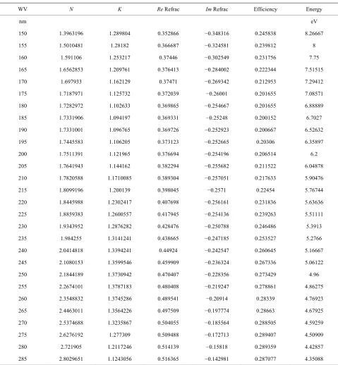
[image:4.595.59.538.109.627.2]As an example, the silicon material file is displayed in
Figure 1. The real and imaginary components of the measured and estimated values are compared with very good agreement. In particular, the elaborate structure of
silicon challenges ones ability to fit it with simple elementary functions like the ones given in Equations (2).
Figure 1. Real (A) and Imaginary(B) Tot( ) using 34 Lo- rentz poles, 4 XLorentz poles and 3 Debye poles.
[image:5.595.68.278.87.236.2]Figure 2. Efficiency Spectrum of planar Silicon. The graph represents the actual percentage of reflection vs. wave- length in nm for a pure silicon slab.
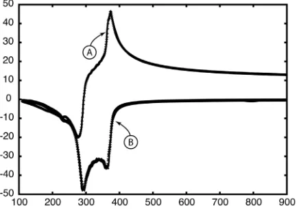
Figure 3. Real (A) and imaginary (B) coefficients of the reflected wave over a thick flat pure silicon.
silicon description is displayed. The two curves represent the real and imaginary amplitude of the relative reflected wave, given explicitly by
1
1
Re N iK N iK and
[image:5.595.65.280.281.431.2]
Figure 4. Real (A,D) and imaginary (B,C) coefficients of the reflected wave over a thick flat pure silicon: A comparison of NIST data and the optimized material file vs. wave energy in eV. As can be seen they are nearly indistinguish- able.
a comparison is exhibited between estimated reflectivity and exact calculation from the data, using analytical expression for both real and imaginary components of the reflected wave. As can be seen, the comparison of the experimental data to the optimized continuous represen- tation is very good. If one wishes, the methodology introduced here can deliver uniform machine accuracy.
3. Other Materials Used in Microchip
Processing
The microchip industry needs the properties of several materials, in addition to crystalline silicon, during the photolithography process. The most critical lossy materi- als are SiO2 (which determines the transistor gate thick-
ness), Si3N4, PolySilicon (which is the actual material on
top of the SiO2 gate) and TiO2. The photolithographic
process is usually confined to a very narrow band width, which requires materials with very tight absorption and refraction properties. However, non-invasive investiga- tion of the results must be performed with a considerably wider bandwidth in order to determine the actual shapes obtained from photolithography, thus assuring the fidel- ity to the original design. As explained above, the precise determination of N and K of materials from narrow band response is technically difficult, resulting in limited data which causes difficulties during optimization. The simple rule of thumb is that the more complicated the N and K
structure of a material, the easier is to obtain reliable dense data vs. wavelength, as seen in the structure of the silicon and PolySilicon curves.
Here we present results for a verification of the mate- rials mentioned. In each, the results contain the permit- tivity (left), the continuous representation of N(A) and
K(B), and the real (A) and imaginary (B) part of the ratio
1
[image:5.595.64.282.483.636.2]of the reflected wave amplitude to the incident wave, given explicitly by Re N iK
1
N iK 1
and
1
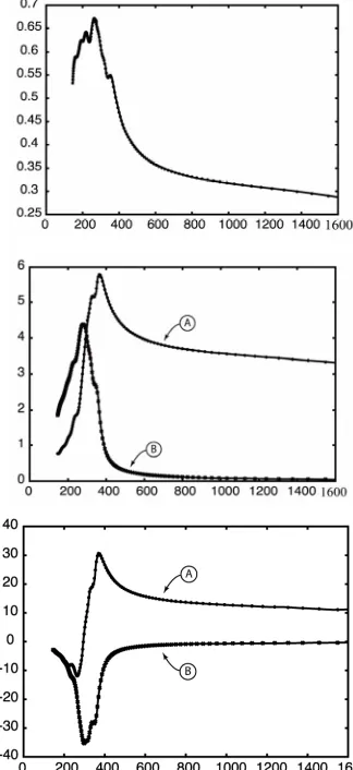
Im N iK N iK 1 respectively. The mate- rial chosen here for a detailed presentation in titanium di- oxide, which participate in the structure of every micro- chip. Again the N and K are displayed in Figure 5, the reflective real and imaginary amplitude in Figure 6 and the efficiency spectrum in Figure 7 respectively.
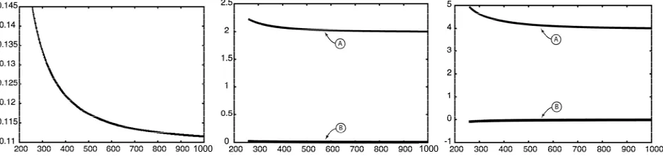
In Figure 8, the properties of crystalline PolySilicon are exhibited. The three graphs are the optimized effi- ciency, N and K and the reflectivity’s real and imaginary parts. In Figures 9 and 10, the very different material properties of SiO2 and Si3N4 are displayed using the
same order of presentation as in PolySilicon (Figure 8).
4. Summary
[image:6.595.321.525.85.229.2]This paper represents a novel methodology to character- ize the optical properties of lossy materials employed in
Figure 5. Real (A) and Imaginary (B) Tot( ) as obtained from the initially measured data of N and K of crystalline titanium di-oxide using 21 Lorentz poles, 3 XLorentz poles and 5 Debye poles.
[image:6.595.339.501.292.645.2]Figure 6. Real (A) and imaginary (B) coefficients of the reflected wave over a thick flat crystalline titanium di-oxide. The graph represents the actual percentage of reflection vs. wave-length in nm for a pure crystalline titanium di-oxide slab.
Figure 7. Efficiency Spectrum of planar crystalline titanium di-oxide. The graph represents the actual percentage of reflection vs. wave-length in nm for a pure crystalline tita- nium di-oxide slab.
Figure 8. Efficiency, real and imaginary permittivity and reflected field of crystalline PolySilicon.
[image:6.595.71.279.321.471.2] [image:6.595.72.277.533.677.2][image:7.595.63.533.86.198.2]
1000 1000
Figure 9. Efficiency, real and imaginary permittivity and reflected field of crystalline SiO2.
1000 1000
Figure 10. Efficiency, real and imaginary permittivity and reflected field of crystalline Si N3 4.
measurements via a cost function. The scheme is very fast and efficient, providing a continuous representation of the optical materials outside the range of measurement, thus enabling broadband direct and inverse scattering calculations and predictions.
5. Acknowledgements
The authors thank the late D. Gottlieb for many helpful discussions and Andrew Abrahamson for technical assis- tance. One of us (EB) dedicates this paper to the de- ceased colleagues and friends Steve A. Orszag, Steve L. Knodle and David Gottlieb.
REFERENCES
[1] S. Abarbanel, D. Gottlieb and J. S. Hesthaven, “Long Time Behavior of the Perfectly Matched Layer Equations in Computational Electromagnetics,” Journal of Scientific
Computing, Vol. 17, No. 1-4, 2002, pp. 405-422. doi:10.1023/A:1015141823608
[2] W. H. Press, B. P. Flannery, S. A. Teukolsky and W. T. Vettering, “Numerical Recipes,” Cambridge University Press, Cambridge, 1986.
[3] E. Barouch, S. L. Knodle and S. A. Orszag, “A Broad-band Electromagnetic Direct and Inverse Scatterin of Nonlinear Lossy Targets,” SPIE Journals, 2013, (in press).
[4] M. Born and E. Wolf, “Principles of Optics,” Pergamon Press, Oxford, 1987.
[5] E. M. Lifshitz, “The Theory of Molecular Attractive For- ces between Solids,” Soviet Physics, Vol. 2, 1956, pp. 73- 83.
[image:7.595.64.534.233.344.2]