Delay Minimization in Multi Level Balanced Interconnect
Tree
Shwetambhri Kaushal
C-DAC, Mohali,India
Vemu Sulochana
C-DAC, Mohali,India
ABSTRACT
This paper presents an effective approach to estimate tree interconnect delays in VLSI circuit designs in deep submicron technologies at high frequencies. In this paper, a symmetrical multi-level interconnect tree network topology has been taken up which consists of elementary resistance, inductance in series with capacitance in parallel. A precise method of modeling symmetrical T-tree interconnect network is effectively examined in this paper. By moment matching fine results are obtained at frequencies as high as 2 GHz at 180 nm technology node.
Keywords
Balanced tree, delay, moment matching, multi-level interconnect, VLSI.
1.
INTRODUCTION
VLSI technology has undergone swift transition from 10 to 20 micron to 24nanomicron technologywhich has resulted in a need of continuous modification of circuits. Any circuit consists of components and interconnects to connect these device components, thus leading to the significance of delays contributed by both.Massive research has been performed in order to forecast the signal integrityof the interconnect networks. These interconnects may have delay of their own due to interconnectcapacitance, discrete capacitance, the interconnect resistance and in long interconnects due inductance effects.
B(0,0) B (0,0)
B (1,0)
B (1,1) N (0,0)
B(2,0)
B(2,1)
B(2,2)
B(2,3) N(1,0)
[image:1.595.309.543.269.362.2]N(1,1) 0)
Figure 1. General RLC interconnect T Tree
As the technology size is shrinking, interconnect delay of high speed digital ICs widely dominate gatedelays.During the transmission of data stream, thesecan besources of signal distortions and asynchronous effects. In this paper, multilevel T tree structure was investigated as shown in Figure 1.
Interconnect tree can be modeled as a distributed RC tree model such as: (i) a lumped capacitor between ground and another node (ii) a lumped resistor between two non ground nodes (iii) an RC line with no direct path to ground (iv) any two RC trees (with common ground) connected together to a non ground
node. In high-speed interconnect design inductance plays a key role in the origin of noise leading to output waveforms which are no longer smooth as in case of RC, thus RLC lines and RLC tree are considered as shown in Figure 2.
Vin Vout
R L
[image:1.595.54.298.531.648.2]C
Interconnect Line
Figure 2. Interconnect as a distributed RLC model
The delay models used to assess interconnect delay in interconnect design have evolved from the simplistic lumped RC model to the sophisticated high order moment matching delay model. As the circuit complexity increases, so does complexity of the interconnections as the case may be for tree networks. Thus more and more accurate and relevant models are needed for the multilevel T-tree interconnections[11]. In this paper the model permits an easy and accurate estimation of signal distortions and losses caused by the balanced tree distribution network at high frequencies.
This paper is further organized as follows –A brief overview of RLC interconnects model and higher order moment matching has been done in the next section. Simulation results and waveforms have been explained in section 3, followed by conclusion in section 4.
2.
BACKGROUND
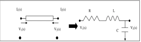
As a signal propagates across a conductor, each new section acts electrically as a small lumped circuit element. In its simplest form, called the lossless model, the equivalent circuit of a transmission line has resistance, inductance and capacitance. These elements are distributed uniformly down the length of the line, as shown in Figure 3. with V1(s), I1(s) as
input voltage and current; and V2(s), I2(s) as output voltage and
current.
I1(s) I2(s)
V1(s) V2(s)
R L
C
V1(s) V2(s)
[image:1.595.310.555.660.733.2]The ABCD matrix for the lossless transmission line [1-2] of length h and characteristic impedance Z0 is
V1 (s)
I1(s) = A BC D
V2(s)
I2(s)
Where ABCD matrix is as given below
A B
C D =
cosh( θh) Z0sinh( θh)
sinh ( θh)
Z0 cosh(θh)
The propagation constant θ = Z(s) ⋅ sC , characteristic impedance Z0 = Z(s) sC andZ s = R + Ls, the per unit
length resistance, inductance and capacitance are denoted by R, L and C respectively [9].
ABCD parameters and their expansions[3] for a distributed RLC transmission line are
A =cosh θh
=1+2!1h2RCs + 2!1h2LC +4!1h4R2C s2+ ⋯(1)
B =Z0sinh( θh)
= Rh + Lh +3!1R2Ch3 s + 2
3!RLCh 3+
5!1h5R3C2 s2+.. (2)
C =sinh ( θh)Z
0
=Chs +3!1C2Rh3s2(3)
D = A (4)
The ABCD matrix values are used to obtain voltage equations at different frequencies in (6) and (7) respectively.
V2(s) = scosh ( R+sL sC )V1 (5)
Equation (5) is used to calculate the output voltage V2(s) at
normal frequency. When the input voltage is 1.8V the output voltage at normal frequency by (5) is 1.805V.
On considering special cases such as output voltage at lower and high frequencies, (5) can be written in terms of RC and LC respectively.
Case-1: Low Frequency; R>> ωL
V2(s) = scosh ( sRC )V1 (6)
At low frequency, considering input V1(s) as 1.8V, output
voltage V2(s) is calculated as 1.82V by using (6).
Case-2: High Frequency; R<< ωL
V2(s) = scosh ( sLC )V1 (7)
At high frequency, considering input V1(s) as 1.8V, output
voltage V2(s) is calculated as 1.85V by substituting V1(s) value
in (7).
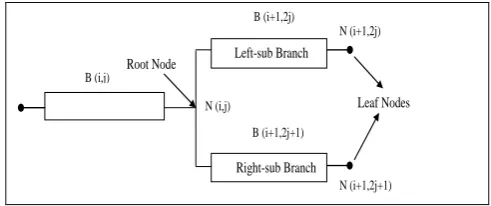
A T-tree can be easily constructed as shown in the Figure 4.
Left-sub Branch
Right-sub Branch B (i,j)
B (i+1,2j)
B (i+1,2j+1) N (i,j)
Root Node
Leaf Nodes N (i+1,2j)
[image:2.595.307.553.71.174.2]N (i+1,2j+1)
Figure 4. T-tree with n=2 levels of index
For a general interconnect tree[4] the total number of levels are denoted by n, this is well explained through Figure 4 where a general interconnect tree with n=2 is shown. The index of a level is represented by i varying from 0 to n-1 [7]. N(i,j), N(0,0) and N(n,j)are the jth node in the ith level, the root node and the leaf node respectively where in j varies from 0 to 2i-1. The load capacitance, CL for the leaf node is denoted as Ci. B(i,j) is the interconnect between leaf node and the previous node. Every node has two sub-branches other than except the leaf node, these sub-branches are the left sub-branch B(i+1,2j) between nodes N(i,j) and N(i+1,2j) ;and the right sub-branch B(i+1,2j+1) which is between nodes N(i,j) and N(i+1,2j+1). The exact delay of an interconnect tree is cumbersome due to complex calculations involved in calculating resistance and inductance values. The total capacitance can be considered to be the sum of all capacitance in the tree i.e. intrinsic or discrete. Thus various methods have been evolved in order to reduce a tree into a linear interconnect so that the delay may be calculated.
It is seen that to calculate delay, Elmore delay utilizes first moment matching of interconnects under the impulse response. For more accurate delay estimation of interconnect, the higher orders of the moment should be considered. In the remaining section, it is shown that how the higher order moments can be efficiently computed. Let h(t) be the impulse response at a node of an interconnect (which may be an RC interconnect, an RLC interconnect, a distributed-RLC or transmission line interconnect). Let v1(t) be the input voltage of the circuit, vn+1(t)
be the output voltage of the node of interest in the circuit, V1(s)
and V N+1(s) be the Laplace transform of v1(t) and v n+1(t)
respectively, the transfer function of h(t) is H(s)=VVN +1(s)
1(s)(8)
Driving point admittance, Y(s) is expressed as
Y(s) = VIN +1 (s)
N +1(s) =
IN +1 (s)
VI(s) H(s) (9) IN+1 (s) is the output current. Expanding Y(s) in terms of the
transfer functions of current and voltages
Y(s) = a1
N +1s+a
2
N +1s2+a
3
N +1s3+⋯…
b0+b1N +1s+b2N +1s2 +b3N +2s3 +⋯..(10)
(10) is the infinite series of driving point admittance in terms of coefficients ak and bk.
Y(s) = ∞i=1Aisi(11)
The summation of infinite series of driving point admittance is
given in (11).
Ai=−1b
0bj
N+1A i−j+ai
N +1
b0 (12)
in terms of the coefficients ak and bk. Equivalent Driving Point Admittance of RLC Model is obtained using (11)
Yeq(s) = sC1 + 1+sC sC2
2(R1 + sL1) (13)
On expanding equation (13)
Yeq s = sCtot+s
2RtotCtot2
3 + s
3 2Rtot2 Ctot3
15 −
LtotCtot2
3 +
⋯ (14)
This simplifies the modeling of the interconnect tree by equating it to an open-ended RLC line with resistance, inductance, and capacitance which are equal to the total interconnect resistance, inductance and capacitance, respectively. It was in turn simplified to a π-model with
R =12Rtot
25 ;L = 12Ltot
25 ;C1= Ctot
6 ;C2= 5Ctot
6 (15)
For moment computation of a tree of transmission lines, many times first each transmission line is modeled as a large number of uniform lumped RLC segments and then the moments of the resulting RLC tree are computed.
3.
EXPERIMENTAL RESULTS
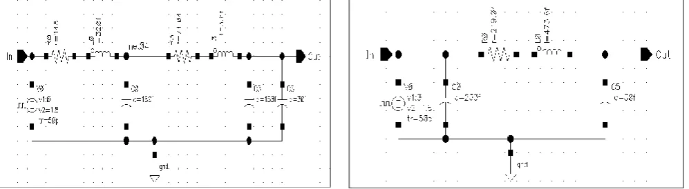
[image:3.595.371.479.71.182.2]In this section, VLSI interconnect design strategy varying at frequencies 0.5GHz to 2GHz is discussed. Here a balanced tree is considered, a balanced tree exhibits identical delay and identical buffer and interconnect segments from the root of the distribution to all branches, due to the structural symmetry. If the matching is strictly followed, structural skew can be zero. The parameter η is introduced to measure the relative asymmetry of a tree. For example, when η is equal to 2, the length of left branches is twice the length of right branches and the load capacitance of the left leaf nodes is twice that of the right leaf nodes, for balanced tree η =1. If interconnect parameters used are R=0.148 Ω/µm, L=0.32 pH/µm, C= 0.18fF/µm and η =1, length of left branch and right branch would be 1000µm and load capacitances in each branch would be 80fF [10]. This tree symmetry is shown in Figure 5 with RLC values stated above.
Figure 5. A symmetrical tree with load capacitances of 80fF load at leaf nodes.
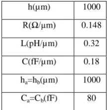
The technology parameters used in the design are given in Table 1.
Table 1 Technology Parameters
Technology(nm) 180
Voltage(V) 1.8
h(µm) 1000
R(Ω/µm) 0.148
L(pH/µm) 0.32
C(fF/µm) 0.18
ha=hb(µm) 1000
Ca=Cb(fF) 80
[image:3.595.311.543.252.397.2]The per unit length resistance, inductance and capacitance are denoted by R, L and C; h is the total interconnect length. Figure 6 shows that the applied input is a square wave at 0.5GHz frequency and the corresponding outputs are considered at root node and leaf nodes.
Figure 6. Input and output waveforms of T-tree at in node, net5, o1 and o2 at 0.5GHz frequency.
Figure 7. Input and output waveforms of T-tree at in node, net5, o1 and o2 at 1 GHz frequency.
[image:3.595.311.544.431.585.2] [image:3.595.55.299.489.654.2]Figure 8. Reduced interconnect segment obtained through higher moment.
Figure 9. Input and output waveforms of two segment interconnect at in node, net 4 and out node at 0.5 GHz frequency.
Figure 10. Input and output waveforms of two segment interconnect at in node, net 4 and out node at 2 GHz frequency.
On analyzing the simulations it is seen that the signal as well as the delay estimate has improved. Now the interconnect
segments is further reduced to RLC segments using basic electrical calculations.
Figure 11. RLC Interconnect as reduced π model.
[image:4.595.59.286.241.401.2]The other simulation parameters considered area stop time varying from 8ns to 120ns, 27C temperature conditions, absolute total voltage and current to be 1µV and 1pA with moderate preset.
Figure 12. Input output waveform of reduced π model on 0.5 GHz frequency.
Figure 13. Input output waveform of reduced π model on 2 GHz frequency.
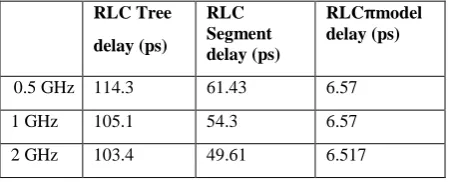
[image:4.595.313.539.284.443.2] [image:4.595.57.288.444.597.2] [image:4.595.311.542.477.634.2]Table 2. Delay at Different Frequencies for 180 nm Technology
RLC Tree
delay (ps)
RLC Segment delay (ps)
RLC𝛑model
delay (ps)
0.5 GHz 114.3 61.43 6.57
1 GHz 105.1 54.3 6.57
2 GHz 103.4 49.61 6.517
First step consists of determination of RLC parameters of each piece of line. Then, the transfer matrix is established of the n-level T-tree network after the design of the single input single output network equivalent to the tree[11]. In the last step, it is possible to calculate the delay and also to analyze output according to the targeted applications of the T-tree network. These results confirm the effectiveness of the proposed method analysis. This analysis can be used by the microelectronic circuit designers notably for the fast and accurate estimation of the distortions caused by the tree network whatever its level number be. The obtained results reveal the effectiveness of the developed circuit by theoretic analysis which is aimed to the global n-level symmetrical RLC-tree network through transfer functions. Thus, it was demonstrated that the established model permits an easy and more accurate estimation of signal distortions and losses caused by the clock tree distribution network.
4.
CONCLUSIONS
The approach followed in this paper permits convenient and accurate estimation of signal distortions and losses caused by the clock tree distribution network. Through the various obtained results using cadence spectre at 180 nm technology node delay in multilevel balanced interconnect tree was analyzed and reduced by 43% even when operating at a high frequency.
5.
ACKNOWLEDGEMENT
A special thanks to C-DAC, Mohali for providing a means to carry out this research work in meticulous way. We are also grateful to MHRD, Govt. of India for providing a platform to do this research work.
6.
REFERENCES
[1] Kahng, A.B.; Muddu, S., "Delay Analysis of VLSI Interconnections Using the Diffusion Equation Model," Design Automation, 1994. 31st Conference on , vol., no., pp.563,569, 6-10 June 1994.
[2] Sahoo, S.; Datta, M.; Kar, R., "An Explicit Delay Model for On-Chip VLSI RLC Interconnect," Devices and Communications (ICDeCom), 2011 International Conference on , vol., no., pp.1,5, 24-25 Feb. 2011.
[3] Kahng, A.B.; Muddu, S., "Efficient gate delay modeling for large interconnect loads," Multi-Chip Module Conference, 1996. MCMC-96, Proceedings., 1996 IEEE , vol., no., pp.202,207, 6-7 Feb 1996.
[4] Ismail, Y.I.; Friedman, E.G., "Effects of inductance on the propagation delay and repeater insertion in VLSI circuits," Very Large Scale Integration (VLSI) Systems, IEEE Transactions on , vol.8, no.2, pp.195,206, April 2000.
[5] Deodhar, V.V.; Davis, J.A., "Optimization of throughput performance for low-power VLSI interconnects," Very Large Scale Integration (VLSI) Systems, IEEE Transactions on , vol.13, no.3, pp.308,318, March 2005.
[6] Saini, S.; Kµmar, A.M.; Veeramachaneni, S.; Srinivas, M.B., "An Alternative approach to Buffer Insertion for Delay and Power Reduction in VLSI Interconnects," VLSI Design, 2010. VLSID '10. 23rd International Conference on , vol., no., pp.411,416, 3-7 Jan. 2010
[7] ITRS, “Interconnect Technology Roadmap for Semiconductors”, 2011 [Online]. Available: http:// public.itrs.net
[8] Xiao-Chun Li; Jun-Fa Mao; Min Tang, "Accurate simulation method for interconnect trees with frequency-dependent transmission line model," Microwave Conference Proceedings, 2005. APMC 2005. Asia-Pacific Conference Proceedings, vol.1, no., pp.2 pp.,, 4-7 Dec.
[9] Kar, R.; Maheshwari, V.; Maqbool, M.; Mondal, S.; Mal, A.K.; Bhattacharjee, A.K., "Crosstalk aware bandwidth modeling for distributed on-chip RLCG interconnects using difference model approach," Computing Communication and Networking Technologies (ICCCNT), 2010 International Conference on , vol., no., pp.1,5, 29-31 July 2010.
[10]Xiao-Chun Li; Jun-Fa Mao; Hui-Fen Huang, "Accurate analysis of interconnect trees with distributed RLC model and moment matching," Microwave Theory and Techniques, IEEE Transactions on , vol.52, no.9, pp.2199,2206, Sept. 2004.