LTC3026
1
3026ff
Typical applicaTion
FeaTures
applicaTions
DescripTion
1.5A Low Input Voltage
VLDO Linear Regulator
The LTC®3026 is a very low dropout (VLDO™) linear
regula-tor that can operate at input voltages down to 1.14V. The device is capable of supplying 1.5A of output current with a typical dropout voltage of only 100mV. To allow opera-tion at low input voltages the LTC3026 includes a boost converter that provides the necessary headroom for the internal LDO circuitry.
Output current comes directly from the input supply to maximize efficiency. The boost converter requires only a small chip inductor and ceramic capacitor for operation. Additionally, the boosted output voltage of one LTC3026 can supply the boost voltage for other LTC3026s, thus requiring a single inductor for multiple LDOs. A user sup-plied boost voltage can be used eliminating the need for an inductor altogether.
The LTC3026 regulator is stable with 10µF or greater ceramic output capacitors. The device has a low 0.4V reference voltage which is used to program the output voltage via two external resistors. The device also has internal current limit, overtemperature shutdown, and reverse output current protection. The LTC3026 is avail-able in a small 10-lead MSOP or low profile (0.75mm) 10-lead 3mm × 3mm DFN package.
1.2V Output Voltage from 1.5V Input Supply
n Input Voltage Range:
1.14V to 3.5V (with Boost Enabled) 1.14V to 5.5V (with External 5V Boost)
n Low Dropout Voltage: 100mV at I
OUT = 1.5A
n Adjustable Output Range: 0.4V to 2.6V n Output Current: Up to 1.5A
n Excellent Supply Rejection Even Near Dropout
n Shutdown Disconnects Load from V
IN and VBST
n Low Operating Current: I
IN = 950µA at VIN = 1.5V
n Low Shutdown Current:
IIN < 1µA (Typ), IBST = 0.1µA (Typ)
n Stable with 10µF or Greater Ceramic Capacitors n Short-Circuit, Reverse Current Protected n Overtemperature Protected
n Available in 10-Lead MSOP and 10-Lead
(3mm × 3mm) DFN Packages
n High Efficiency Linear Regulator n Post Regulator for Switching Supplies n Microprocessor Supply
Dropout Voltage vs Output Current
SW
IN 0.4V
OUT BST 5V BOOST CONVERTER
GND
ADJ
PG L1
10µH
4.7µF
COUT 10µF VIN = 1.5V
VOUT = 1.2V, 1.5A
OFF ON
100k 8.06k
4.02k LTC3026
3026 TA01a
SHDN
L1: MURATA LQH2MCN100K02 +
–
4.7µF
IOUT (A) 0
DROPOUT (mV)
100 150
3026 TA01b 50
0
0.5 1.0 1.5
1.2V 1.5V 2.0V 2.6V L, LT, LTC, LTM, Linear Technology, the Linear logo and Burst Mode are registered trademarks
and ThinSOT, VLDO are trademarks of Linear Technology Corporation. All other trademarks are the property of their respective owners.
LTC3026
2
3026ff
absoluTe MaxiMuM raTings
VBST to GND ... –0.3V to 6V VIN to GND ... –0.3V to 6V PG to GND ... –0.3V to 6V
SHDN to GND ... –0.3V to 6.3V ADJ to GND ... –0.3V to (VIN + 0.3V)
(Note 1)
TOP VIEW
DD PACKAGE
10-LEAD (3mm × 3mm) PLASTIC DFN
10 9
6 7 8 4
5 3 2
1 OUT
OUT ADJ PG
SHDN
IN IN GND SW BST
11 GND
TJMAX = 125°C, θJA = 40°C/W
EXPOSED PAD (PIN 11) IS GND, MUST BE SOLDERED TO PCB
1 2 3 4 5 IN IN GND SW BST
10 9 8 7 6
OUT OUT ADJ PG
SHDN
TOP VIEW
MSE PACKAGE 10-LEAD PLASTIC MSOP
11 GND
TJMAX = 125°C, θJA = 40°C/W
EXPOSED PAD (PIN 11) IS GND, MUST BE SOLDERED TO PCB
pin conFiguraTion
orDer inForMaTion
LEAD FREE FINISH TAPE AND REEL PART MARKING PACKAGE DESCRIPTION TEMPERATURE RANGE
LTC3026EDD#PBF LTC3026EDD#TRPBF LBHW 10-Lead (3mm × 3mm) Plastic DFN –40°C to 125°C LTC3026IDD#PBF LTC3026IDD#TRPBF LBHW 10-Lead (3mm × 3mm) Plastic DFN –40°C to 125°C LTC3026EMSE#PBF LTC3026EMSE#TRPBF LTBJB 10-Lead Plastic MSOP –40°C to 125°C LTC3026IMSE#PBF LTC3026IMSE#TRPBF LTBJB 10-Lead Plastic MSOP –40°C to 125°C
LEAD BASED FINISH TAPE AND REEL PART MARKING PACKAGE DESCRIPTION TEMPERATURE RANGE
LTC3026EDD LTC3026EDD#TR LBHW 10-Lead (3mm × 3mm) Plastic DFN –40°C to 125°C LTC3026IDD LTC3026IDD#TR LBHW 10-Lead (3mm × 3mm) Plastic DFN –40°C to 125°C LTC3026EMSE LTC3026EMSE#TR LTBJB 10-Lead Plastic MSOP –40°C to 125°C LTC3026IMSE LTC3026IMSE#TR LTBJB 10-Lead Plastic MSOP –40°C to 125°C Consult LTC Marketing for parts specified with wider operating temperature ranges.
For more information on lead free part marking, go to: http://www.linear.com/leadfree/ For more information on tape and reel specifications, go to: http://www.linear.com/tapeandreel/
Output Short-Circuit Duration ... Indefinite Operating Junction Temperature Range
(Note 8) ... –40°C to 125°C Storage Temperature Range ... –65°C to 125°C Lead Temperature (MSE, Soldering, 10 sec) ...300°C
LTC3026
3
3026ff
elecTrical characTerisTics
The l denotes the specifications which apply over the full operating junction temperature range, otherwise specifications are at
TJ = 25°C. VIN = 1.5V, VOUT = 1.2V, CIN = CBST = 4.7µF, COUT = 10µF (all capacitors ceramic) unless otherwise noted.
(BOOST ENABLED, LSW = 10µH)
SYMBOL PARAMETER CONDITIONS MIN TYP MAX UNITS
VIN Operating Voltage (Note 2) l 1.14 5.5 V
IIN Operating Current IOUT = 100µA, VSHDN = VIN, 1.2V ≤ VIN ≤ 5V l 95 200 µA
IINSHDN Shutdown Current VSHDN = 0V, VIN = 3.5V l 0.6 20 µA
VBST Boost Operating Voltage (Note 7) VSHDN = VIN l 4.5 5 5.5 V
VBSTUVLO Undervoltage Lockout l 4.0 4.25 4.4 V
IBST Boost Operating Current IOUT = 100µA, VSHDN = VIN l 175 275 µA
IBSTSHDN Boost Shutdown Current VSHDN = 0V 1 5 µA The l denotes the specifications which apply over the full operating junction temperature range, otherwise specifications are at
TJ = 25°C. VIN = 1.5V, VOUT = 1.2V, VBST = 5V, CIN = CBST = 1µF, COUT = 10µF (all capacitors ceramic) unless otherwise noted.
(BOOST DISABLED, VSW = 0V or Floating)
SYMBOL PARAMETER CONDITIONS MIN TYP MAX UNITS
VADJ Regulation Voltage (Note 5) 1mA ≤ IOUT ≤ 1.5A, 1.14V ≤ VIN ≤ 3.5V, VBST = 5V, VOUT = 0.8V
1mA ≤ IOUT ≤ 1.5A, 1.14V ≤ VIN ≤ 3.5V, VBST = 5V, VOUT = 0.8V l
0.397
0.395 0.4 0.4 0.403 0.405 V V OUT Programming Range l 0.4 2.6 V
Dropout Voltage (Note 6) VIN = 1.5V, VADJ = 0.38, IOUT = 1.5A l 100 250 mV
IADJ ADJ Input Current VADJ = 0.4V l –100 100 nA
IOUT Continuous Output Current VSHDN = VIN l 1.5 A
ILIM Output Current Current Limit 3 A
en Output Voltage Noise f = 10Hz to 100kHz, IL = 800mA
Boost Disabled
Boost Enabled 110 210 µVµVRMS RMS The l denotes the specifications which apply over the full operating junction temperature range, otherwise specifications are at
TJ = 25°C. VIN = 1.5V, VOUT = 1.2V, CIN = CBST = 1µF, COUT = 10µF (all capacitors ceramic) unless otherwise noted.
(BOOST ENABLED or DISABLED)
SYMBOL PARAMETER CONDITIONS MIN TYP MAX UNITS
VIN Operating Voltage (Note 2) l 1.14 3.5 V
IIN Operating Current IOUT = 0mA, VOUT = 0.8V, VSHDN = VIN, VIN = 1.2V
IOUT = 0mA, VOUT = 1.2V, VSHDN = VIN, VIN = 1.5V
IOUT = 0mA, VOUT = 1.2V, VSHDN = VIN, VIN = 2.5V
IOUT = 0mA, VOUT = 1.2V, VSHDN = VIN, VIN = 3.5V
1160 950 640 400
µA µA µA µA IINSHDN Shutdown Current VSHDN = 0V, VIN = 3.5V l 0.6 20 µA
Inductor Size Requirement
Inductor Peak Current Requirement 1504.7 10 40 mAµH VBST Boost Output Voltage Range VSHDN = VIN 4.8 5 5.2 V
VBSTUVLO Boost Undervoltage Lockout l 4.0 4.2 4.4 V
Boost Output Drive (Note 3) VIN < 1.4V
VIN ≥ 1.4V
7
LTC3026
4
3026ff
IN Supply Current with Boost
Converter Enabled BST Supply Current with Boost Converter Disabled IN Supply Current with Boost Converter Disabled
Typical perForMance characTerisTics
elecTrical characTerisTics
Note 1: Stresses beyond those listed under Absolute Maximum Ratings
may cause permanent damage to the device. Exposure to any Absolute Maximum Rating condition for extended periods may affect device reliability and lifetime. This IC has overtemperature protection that is intended to protect the device during momentary overload conditions. Junction temperatures will exceed 125°C when overtemperature is active. Continuous operation above the specified maximum operating junction temperature may impair device reliability.
Note 2: Minimum Operating Voltage required for regulation is:
VIN ≥ VOUT(MIN) + VDROPOUT
Note 3: When using BST to drive loads other than LTC3026s, the load
must be high impedance during start-up (i.e. prior to PG going high).
Note 4: PG threshold expressed as a percentage difference from the
“VADJ Regulation Voltage” as given in the table.
Note 5: Operating conditions are limited by maximum junction temperature.
The regulated output voltage specification will not apply for all possible combinations of input voltage and output current. When operating at maximum input voltage, the output current range must be limited. When operating at maximum output current, the input voltage range must be limited.
Note 6: Dropout voltage is minimum input to output voltage differential
needed to maintain regulation at a specified output current. In dropout, the output voltage will be equal to VIN – VDROPOUT.
Note 7: To maintain correct regulation
VOUT ≤ VBST – 2.4V
Note 8: The LTC3026 is tested under pulsed load conditions such
that TJ ≈ TA. The LTC3026E is guaranteed to meet specifications from
0°C to 125°C junction temperature. Specifications over the –40°C to 125°C operating junction temperature range are assured by design, characterization and correlation with statistical process controls. The LTC3026I is guaranteed over the –40°C to 125°C operating junction temperature range. Note that the maximum ambient temperature consistent with these specifications is determined by specific operating conditions in conjunction with board layout, the rated package thermal impedance and other environmental factors. The junction temperature (TJ, in °C) is calculated from the ambient temperature (TA, in °C) and
power dissipation (PD, in watts) according to the formula:
TJ = TA + (PD • θJA), where θJA (in °C/W) is the package thermal
impedance.
3026 G01
VIN (V)
1.0
INPUT CURRENT (mA)
1.50 1.25 1.00 0.75 0.50 0.25 0
1.5 2.0 2.5 3.0 3.5
–40°C 25°C 85°C
3026 G02
VIN (V)
1.0
IBST
(µA)
5.5 4.0 4.5 5.0
1.5 2.0 2.5 3.0 3.5
200
150
100
50
0
–40°C 25°C 85°C 125°C VBST = 5V
3026 G03
VIN (V)
1.0 1.5 2.0 2.5 3.0 3.5 4.0 4.5 5.0 5.5
IIN
(µA)
200
150
100
50
0
–40°C 25°C 85°C 125°C VBST = 5V
The l denotes the specifications which apply over the full operating junction temperature range, otherwise specifications are at
TJ = 25°C. VIN = 1.5V, VOUT = 1.2V, CIN = CBST = 1µF, COUT = 10µF (all capacitors ceramic) unless otherwise noted.
(BOOST ENABLED or DISABLED)
SYMBOL PARAMETER CONDITIONS MIN TYP MAX UNITS
VIHSHDN SHDN Input High Voltage 1.14V ≤ VIN ≤ 3.5V
3.5V ≤ VIN ≤ 5.5V
l l
1.0
1.2 V V VILSHDN SHDN Input Low Voltage 1.14V ≤ VIN ≤ 5.5V l 0.4 V
IIHSHDN SHDN Input High Current SHDN = VIN –1 1 µA
IILSHDN SHDN Input Low Current SHDN = 0V –1 1 µA
VOLPG PG Output Low Voltage IPG = 2mA l 0.1 0.4 V
IOHPG PG Output High Leakage Current VPG = 5.5V 0.01 1 µA
PG Output Threshold (Note 4) PG High to Low
LTC3026
5
3026ff
ADJ Voltage vs Temperature IN Shutdown Current BST Voltage vs Temperature
Typical perForMance characTerisTics
Dropout Voltage vs Input Voltage Ripple Rejection Ripple Rejection
Shutdown Threshold Output Current Limit BST to OUT Headroom Voltage
3026 G04 TEMPERATURE (°C) –50 –25 404 403 402 401 400 399 398 397 396 75 100
0 25 50 125
ADJUST VOLTAGE (mV)
1mA 1.5A
VBST = 5V
VIN = 1.5V
VOUT =1.2V
3026 G05
–50 –25 0 25 50 75 100 125
TEMPERATURE (°C)
INPUT CURRENT (µA)
5.0 4.5 4.0 3.5 3.0 2.5 2.0 1.5 1.0 0.5 0 1.2V 2.5V 3.5V 3026 G06
–50 –25 0 25 50 75 100 125
TEMPERATURE (°C) 5.050 5.025 5.000 4.975 4.950
BST VOLTAGE (V)
VIN = 1.5V
3026 G07
VIN (V)
1.2 200 180 160 140 120 100 80 60 40 20 0 2.2
1.4 1.6 1.8 2.0 2.4 2.6
DROPOUT (mV)
–40°C 25°C 85°C 125°C VFB = 0.38V
IOUT =1.5A
3026 G08
VIN (V)
1.2
RIPPLE REJECTION (dB)
60 50 40 30 20 10 0 1.8 2.2
1.4 1.6 2.0 2.4 2.6
1MHz 100kHz
10kHz
VBST = 5V
VOUT =1.2V
IOUT = 800mA
COUT = 10µF
3026 G09 FREQUENCY (Hz) 100 70 60 50 40 30 20 10 0 100000
1000 10000 1000000 1E+07
RIPPLE REJECTION (dB) VVBSTIN = 1.5V = 5V
VOUT =1.2V
IOUT = 800mA
COUT = 10µF
3026 G10
VIN (V)
1 VSHDN THRESHOLD (mV) 1200 900 600 300
2 3 4 5 6
–40°C 25°C 125°C RISE RISE RISE FALL FALL FALL 3026 G11
VIN (V)
1.0
IOUT
(A)
2.5 3.5
1.5 2.0 3.0
5.0 4.5 4.0 3.5 3.0 2.5 2.0 1.5 1.0 CURRENT LIMIT THERMAL LIMIT VOUT = 0V
TA = 25°C
3026 G12 TEMPERATURE (°C) –50 VBST – V OUT (V) 2.22 2.20 2.18 2.16 2.14 2.12 2.10 2.08 2.06 2.04 2.02
0 50 75
LTC3026
6
3026ff
Typical perForMance characTerisTics
IN Supply Transient Response BST/OUT Start-Up BST Ripple and Feedthrough to OUT
3026 G16
VIN
2V 1.5V
VOUT
AC 10mV/DIV
10µs/DIV VOUT = 1.2V
IOUT = 800mA
COUT = 10µF
VBST = 5V
TA = 25°C
3026 G17 SHDN
BST
OUT HI LO
200µs/DIV TA = 25°C
ROUT = 1Ω
VIN = 1.7V
5V
1.5V 1V
0V
3026 G18
VBST
AC 20mV/DIV
VOUT
AC 5mV/DIV
20µs/DIV VOUT = 1.2V
VIN = 1.5V
IOUT = 1A
COUT = 10µF
LSW = 10µH
TA = 25°C
Delay from Enable to PG with
Boost Disabled Delay from Enable to PG with Boost Enabled Output Load Transient Response
3026 G13
VIN (V)
1.0
DELAY (µs)
2.0 3.0 3.5 5.5
1.5 2.5 4.0 4.5 5.0
400 375 350 325 300 275 250
–40°C 25°C 85°C VOUT = 0.8V
ROUT = 8Ω
3026 G14
VIN (V)
1.0
DELAY (ms)
5.0 4.5 4.0 3.5 3.0 2.5 2.0 1.5 1.0 0.5 0
3.0
1.5 2.0 2.5 3.5
–40°C 25°C 85°C VOUT = 0.8V
ROUT = 8Ω
3026 G15
IOUT
1.5A 2mA
OUT AC 20mV/DIV
50µs/DIV VOUT = 1.5V
COUT = 10µF
VIN = 1.7V
LTC3026
7
3026ff
pin FuncTions
IN (Pins 1, 2): Input Supply Voltage. Output load current
is supplied directly from IN. The IN pin should be locally bypassed to ground if the LTC3026 is more than a few inches away from another source of bulk capacitance. In general, the output impedance of a battery rises with frequency, so it is usually advisable to include an input bypass capacitor when supplying IN from a battery. A capacitor in the range of 0.1µF to 4.7µF is usually sufficient.
GND (Pin 3, Exposed Pad Pin 11): Ground and Heat Sink.
Connect the exposed pad to the PCB ground plane or large pad for optimum thermal performance.
SW (Pin 4): Boost Switching Pin. This is the boost converter
switching pin. A 4.7µH to 40µH inductor able to handle a peak current of 150mA is connected from this pin to VIN. The boost converter can be disabled by floating this pin. This allows the use of an external boosted supply from a second LTC3026 or other source. See Operating with Boost Converter Disabled section for more information.
BST (Pin 5): Boost Output Voltage Pin. With boost
con-verter enabled bypass the BST pin with a ≥4.7µF low ESR ceramic capacitor to GND (CBST). BST does not load VIN when in shutdown, but is diode connected to IN through the external inductor, thus, will not go to ground with VIN present. Users should not present any loads to the BST pin (with boost enabled) until PG signals that regulation
has been achieved. When providing an external BST volt-age (i.e. boost converter disabled) a 1µF low ESR ceramic capacitor can be used.
SHDN (Pin 6): Shutdown Input Pin, Active Low. This pin
is used to put the LTC3026 into shutdown. The SHDN pin current is typically less than 10nA. The SHDN pin cannot be left floating and must be tied to a valid logic level (such as IN) if not used.
PG (Pin 7): Power Good Pin. When PG is high impedance
OUT is in regulation, and low impedance when OUT is in shutdown or out of regulation.
ADJ (Pin 8): Output Adjust Pin. This is the input to the error
amplifier. It has a typical bias current of 0.1nA flowing into the pin. The ADJ pin reference voltage is 0.4V referenced to ground. The output voltage range is 0.4V to 2.6V and is typically set by connecting ADJ to a resistor divider from OUT to GND. See Figure 2.
OUT (Pins 9, 10): Regulated Output Voltage. The OUT pins
supply power to the load. A minimum output capacitance of 5µF is required to ensure stability. Larger output capaci-tors may be required for applications with large transient loads to limit peak voltage transients. See the Applica-tions Information section for more information on output capacitance.
LTC3026
8
3026ff –
+
– +
– +
– +
SWITCHING
LOGIC EN
SHDN
0.4V REFERENCE
BOOST CONVERTER
6
7
4 5
8 UVLO
1,2 SW
IN
OUT BST
SHDN
ADJ
PG 9,10
0.372V
3026 BD
GND 3,11
+ –
OVERSHOOT DETECT VOFF
LTC3026
9
3026ff
The LTC3026 is a VLDO (very low dropout) linear regulator which operates from input voltages as low as 1.14V. The LDO uses an internal NMOS transistor as the pass device in a source-follower configuration. The BST pin provides the higher supply necessary for the LDO circuitry while the output current comes directly from the IN input for high efficiency regulation. The BST pin can either be supplied off-chip by an external 5V source or it can be generated through the internal boost converter of the LTC3026.
Boost Converter Operation
For applications where an external 5V supply is not avail-able, the LTC3026 contains an internal boost converter to produce the necessary 5V supply for the LDO. The boost converter utilizes Burst Mode® operation to achieve high efficiency for the relatively low current levels needed for the LDO circuitry. The boost converter requires only a small chip inductor between the IN and SW pins and a small 4.7µF capacitor at BST.
The operation of the boost converter is described as fol-lows. During the first half of the switching cycle, an internal NMOS switch between SW and GND turns on, ramping the inductor current. A peak comparator senses when the inductor current reaches 100mA, at which point the NMOS is turned off and an internal PMOS between SW and BST turns on, transferring the inductor current to the BST pin. The PMOS switch continues to deliver power to BST until the inductor current approaches zero, at which point the PMOS turns off and the NMOS turns back on, repeating the switching cycle.
A burst comparator with hysteresis monitors the voltage on the BST pin. When BST is above the upper threshold of the comparator, no switching occurs. When BST falls below the comparator’s lower threshold, switching com-mences and the BST pin gets charged. The upper and lower thresholds of the burst comparator are set to maintain a 5V supply at BST with approximately 40mV to 50mV of ripple.
Care must be taken not to short the BST pin to GND, since the body diode of the internal PMOS transistor connects the BST and SW pins. Shorting BST to GND with an induc-tor connected between IN and SW can ramp the inducinduc-tor current to destructive levels, potentially destroying the inductor and/or the part.
Operating with Boost Converter Disabled
The LTC3026 has an option to disable the internal boost converter. With the boost converter disabled, the LTC3026 becomes a bootstrapped device and the BST pin must be driven by an external 5V supply, or driven by the BST pin of a second LTC3026 with the boost converter enabled. The recommended method for disabling the boost converter is to simply float the SW pin. With the SW pin floating no energy can be transferred to BST which effectively disables the boost converter.
A single LTC3026 boost converter can be used to drive multiple bootstrapped LTC3026s with the internal boost converters disabled. Thus a single inductor can be used to power two (or possibly more) functioning LTC3026s. In cases where all LTC3026s have the same input supply (IN) the internal boost converters of the bootstrapped LTC3026s can be disabled by floating the SW pin. If the LTC3026s are not all connected to the same input supply then the internal boost converters of the bootstrapped LTC3026s are disabled by floating the SW pin.
LDO Operation
An undervoltage lockout comparator (UVLO) senses the BST pin voltage to ensure that the bias supply for the LDO is greater than 4.2V before enabling the LDO. If BST is below 4.2V, the UVLO shuts down the LDO, and OUT is pulled to GND through the external divider.
LTC3026
10
3026ff
operaTion
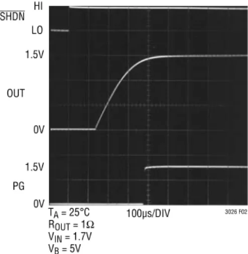
Figure 1. Output Load Step Response
The LDO provides a high accuracy output capable of supplying 1.5A of output current with a typical dropout voltage of only 100mV. A single ceramic capacitor as small as 10µF is all that is required for output bypassing. A low reference voltage allows the LTC3026 output to be programmed to much lower voltages than available in common LDOs (range of 0.4V to 2.6V).
The devices also include current limit and thermal overload protection, and will survive an output short-circuit indefi-nitely. The fast transient response of the follower output stage overcomes the traditional trade-off between dropout voltage, quiescent current and load transient response
inherent in most LDO regulator architectures, see Figure 1. Figure 2. Soft-Start with Boost Disable
Figure 3. Programming the LTC3026
IOUT
1.5A 0mA
OUT AC 20mV/DIV
100µs/DIV VOUT = 1.5V
COUT = 10µF
VIN = 1.7V
VB = 5V
3026 F01
SHDN
OUT
PG HI LO
100µs/DIV TA = 25°C
ROUT = 1Ω
VIN = 1.7V
VB = 5V
1.5V
1.5V 0V
0V
3026 F02
VOUT
ADJ GND
COUT
R2 R1 LTC3026
3026 F03
VOUT=0.4V 1+ R2R1
The LTC3026 also includes a soft-start feature to prevent excessive current flow at VIN during start-up. When the LDO is enabled, the soft-start circuitry gradually increases the LDO reference voltage from 0V to 0.4V over a period of approximately 200µs, see Figure 2.
Adjustable Output Voltage
The output voltage is set by the ratio of two external resis-tors as shown in Figure 3. The device servos the output to maintain the ADJ pin voltage at 0.4V (referenced to ground). Thus, the current in R1 is equal to 0.4V/R1. For good transient response, stability and accuracy the current in R1 should be at least 80µA, thus, the value of R1 should be no greater than 5k. The current in R2 is the current in R1 plus the ADJ pin bias current. Since the ADJ pin bias current is typically <10nA it can be ignored in the output voltage calculation. The output voltage can be calculated using the formula in Figure 3. Note that in shutdown the output is turned off and the divider current will be zero once COUT is discharged.
LTC3026
11
3026ff
operaTion
The LTC3026 operates at a relatively high gain of 270µV/A referred to the ADJ input. Thus, a load current change of 1mA to 1.5A produces a 400µV drop at the ADJ input. To calculate the change in the output, simply mul-tiply by the gain of the feedback network (i.e. 1 + R2/R1). For example, to program the output for 1.2V choose R2/R1 = 2. In this example an output current change of 1mA to 1.5A produces –400µV • (1 + 2) = 1.2mV drop at the output.
Power Good Operation
The LTC3026 includes an open-drain power good (PG) output pin with hysteresis. If the chip is in shutdown or under UVLO conditions (VBST < 4.25V), PG is low im-pedance to ground. PG becomes high imim-pedance when VOUT rises to 93% of its regulation voltage. PG stays high impedance until VOUT falls back down to 91% of its regula-tion value. A pull-up resistor can be inserted between PG and a positive logic supply (such as IN, OUT, BST, etc.) to signal a valid power good condition. VIN should be the minimum operating voltage (1.14V) or greater for PG to function correctly.
Output Capacitance and Transient Response
The LTC3026 is designed to be stable with a wide range of ceramic output capacitors. The ESR of the output capacitor affects stability, most notably with small ca-pacitors. An output capacitor of 10µF or greater with an ESR of 0.05Ω or less is recommended to ensure stability.
The LTC3026 is a micropower device and output transient response will be a function of output capacitance. Larger values of output capacitance decrease the peak deviations and provide improved transient response for larger load current changes. Note that bypass capacitors used to decouple individual components powered by the LTC3026 will increase the effective output capacitor value. High ESR tantalum and electrolytic capacitors may be used, but a low ESR ceramic capacitor must be in parallel at the output. There is no minimum ESR or maximum capacitor size requirements.
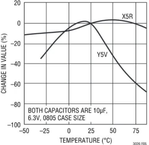
Extra consideration must be given to the use of ceramic capacitors. Ceramic capacitors are manufactured with a variety of dielectrics, each with different behavior across temperature and applied voltage. The most common di-electrics used are Z5U, Y5V, X5R and X7R. The Z5U and Y5V dielectrics are good for providing high capacitances in a small package, but exhibit strong voltage and tem-perature coefficients as shown in Figures 4 and 5. When used with a 2V regulator, a 10µF Y5V capacitor can exhibit an effective value as low as 1µF to 2µF over the operating temperature range. The X5R and X7R dielectrics result in more stable characteristics and are more suitable for use as the output capacitor. The X7R type has better stability across temperature, while the X5R is less expensive and is available in higher values.
A minimum capacitance of 5µF must be maintained at all times on the LTC3026 LDO output.
Figure 4. Ceramic Capacitor DC Bias Characteristics Figure 5. Ceramic Capacitor Temperature Characteristics
DC BIAS VOLTAGE (V)
CHANGE IN V
ALUE (%)
3026 F04
20 0 –20 –40 –60 –80 –100
X5R
Y5V
BOTH CAPACITORS ARE 10µF, 6.3V, 0805 CASE SIZE
0 1 2 3 4 5 6
TEMPERATURE (°C) –50
20 0 –20 –40 –60 –80 –100
25 75
3026 F05
–25 0 50
Y5V
CHANGE IN VALUE (%)
X5R
BOTH CAPACITORS ARE 10µF, 6.3V, 0805 CASE SIZE
LTC3026
12
3026ff
operaTion
Boost Converter Component Selection
A 10µH chip inductor with a peak saturation current (ISAT) of at least 150mA is recommended for use with the internal boost converter. The inductor value can range between 4.7µH to 40µH, but values less than 10µH result in higher switching frequency, increased switching losses, and lower max output current available at the BST pin. See Table 1 for a list of component suppliers.
Table 1. Inductor Vendor Information
SUPPLIER PART NUMBER WEBSITE
Coilcraft 0603PS-103KB www.coilcraft.com Murata LQH2MCN100K02 www.murata.com Taiyo Yuden LB2016T100M www.t-yuden.com TDK NLC252018T-100K www.TDK.com
It is also recommended that the BST pin be bypassed to ground with a 4.7µF or greater ceramic capacitor. Larger values of capacitance will not reduce the size of the BST ripple much, but will decrease the ripple frequency propor-tionally. The BST pin should maintain 1µF of capacitance at all times to ensure correct operation (See the “Output Capacitance and Transient Response” section about capacitor selection). High ESR tantalum and electrolytic capacitors may be used, but a low ESR ceramic must be used in parallel for correct operation.
Thermal Considerations
The power handling capability of the device will be limited by the maximum rated junction temperature (125°C). The majority of the power dissipated in the device will be the output current multiplied by the input/output voltage differential: (IOUT)(VIN – VOUT). Note that the BST current is less than 200µA even under heavy loads, so its power consumption can be ignored for thermal calculations. The LTC3026 has internal thermal limiting designed to protect the device during momentary overload conditions. For continuous normal conditions, the maximum junction temperature rating of 125°C must not be exceeded. It is important to give careful consideration to all sources of thermal resistance from junction to ambient. Additional heat sources mounted nearby must also be considered.
For surface mount devices, heat sinking is accomplished by using the heat-spreading capabilities of the PC board and its copper traces. Copper board stiffeners and plated through holes can also be used to spread the heat gener-ated by power devices.
A junction-to-ambient thermal coefficient of 40°C/W is achieved by connecting the exposed pad of the MSOP or DFN package directly to a ground plane of about 2500mm2.
Calculating Junction Temperature
Example: Given an output voltage of 1.2V, an input voltage of 1.8V ±4%, an output current range of 0mA to 1A and a maximum ambient temperature of 50°C, what will the maximum junction temperature be?
The power dissipated by the device will be approximately:
IOUT(MAX)(VIN(MAX) – VOUT)
where:
IOUT(MAX) = 1A
VIN(MAX) = 1.87V
so:
P = 1A(1.87V – 1.2V) = 0.67W
Even under worst-case conditions LTC3026’s BST pin power dissipation is only about 1mW, thus can be ignored. The junction to ambient thermal resistance will be on the order of 40°C/W. The junction temperature rise above ambient will be approximately equal to:
0.67W(40°C/W) = 26.8°C
The maximum junction temperature will then be equal to the maximum junction temperature rise above ambient plus the maximum ambient temperature or:
TA = 26.8°C + 50°C = 76.8°C
Short-Circuit/Thermal Protection
The LTC3026 has built-in output short-circuit current limiting as well as overtemperature protection. During short-circuit conditions, internal circuitry automatically limits the output current to approximately 3A. At higher
LTC3026
13
3026ff
operaTion
temperatures, or in cases where internal power dissipa-tion cause excessive self heating on-chip, the thermal shutdown circuitry will shut down the boost converter and LDO when the junction temperature exceeds approximately 150°C. It will reenable the converter and LDO once the junction temperature drops back to approximately 140°C. The LTC3026 will cycle in and out of thermal shutdown without latchup or damage until the overstress condition is removed. Long term overstress (TJ > 125°C) should be avoided as it can degrade the performance or shorten the life of the part.
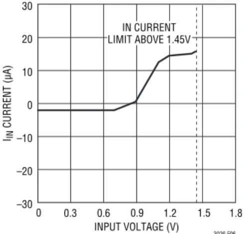
Reverse Input Current Protection
The LTC3026 features reverse input current protection to limit current draw from any supplementary power source at the output. Figure 6 shows the reverse output current limit for constant input and output voltages cases. Note: Positive input current represents current flowing into the VIN pin of LTC3026.
With VOUT held at or below the output regulation voltage and VIN varied, IN current flow will follow Figure 6’s curves. IIN reverse current ramps up to about 16µA as the VIN approaches VOUT. Reverse input current will spike up as VIN approaches within about 30mV of VOUT as the reverse current protection circuitry is disabled and normal opera-tion resumes. As VIN transitions above VOUT the reverse current transitions into short-circuit current as long as VOUT is held below the regulation voltage.
Layout Considerations
Connection from BST and OUT pins to their respec-tive ceramic bypass capacitor should be kept as short as possible. The ground side of the bypass capacitors should be connected directly to the ground plane for best results or through short traces back to the GND pin of the part. Long traces will increase the effective series ESR and inductance of the capacitor which can degrade performance.
With the boost converter enabled, the SW pin will be switching between ground and 5V whenever the BST pin needs to be recharged. The transition edge rates of the SW pin can be quite fast (~10ns). Thus care must be taken to make sure the SW node does not couple capacitively to other nodes (especially the ADJ pin). Additionally, stray capacitance to this node reduces the efficiency and amount of current available from the boost converter. For these reasons it is recommended that the SW pin be connected to the switching inductor with as short a trace as possible. If the user has any sensitive nodes near the SW node, a ground shield may be placed between the two nodes to reduce coupling.
Because the ADJ pin is relatively high impedance (depend-ing on the resistor divider used), stray capacitance at this pin should be minimized (<10pF) to prevent phase shift in the error amplifier loop. Additionally special attention should be given to any stray capacitances that can couple external signals onto the ADJ pin producing undesirable output ripple. For optimum performance connect the ADJ pin to R1 and R2 with a short PCB trace and minimize all other stray capacitance to the ADJ pin.
Figure 6. Input Current vs Input Voltage Figure 7. Suggested Layout
1 2 3 4 5
10 9 8 7 6 IN
IN GND SW BST
OUT OUT ADJ PG
SHDN 3026 F07
VIA CONNECTION TO GND PLANE
CIN COUT
LSW
CBST
R2 R1
INPUT VOLTAGE (V)
IIN
CURRENT (µA)
3026 F06
30 20 10 0 –10 –20 –30
0 0.3 0.6 0.9 1.2 1.5 1.8
IN CURRENT LIMIT ABOVE 1.45V
LTC3026
14
3026ff
Typical applicaTions
Using 1 Boost with Multiple Regulators
2.5V Output from 3.3V Supply with External 5V Bias IN
SW
OUT BST
GND
ADJ
PG 10µH
4.7µF
COUT1 10µF VIN = 2.5V
VOUT1 1.8V, 1.5A
PG1 PG2
100k 14k
4.02k LTC3026
3026 TA02 SHDN
LTC3026 WITH BOOST ENABLED FANOUT: 3-LTC3026 FOR VIN <1.4V
5-LTC3026 FOR VIN >1.4V
BOOT STRAPPED LTC3026 (BOOST DISABLED) 4.7µF
IN SW NC
OUT BST
GND
ADJ
PG 1µF
COUT2 10µF
VOUT2 1.5V, 1.5A
100k 11k
4.02k LTC3026
SHDN
1µF
TO ADDITIONAL REGULATORS
PG
3026 TA03 IN
SW*
OUT BST
GND
ADJ
PG
1µF
COUT
10µF VOUT
2.5V, 1.5A
100k 21k
4.02k LTC3026
SHDN
1µF VBIAS = 5V
N/C VIN = 3.3V
* SEE OPERATING WITH BOOST CONVERTER DISABLED SECTION FOR INFORMATION ON DISABLING BOOST CONVERTER.
LTC3026
15
3026ff MSOP (MSE) 0911 REV H
0.53 ±0.152 (.021 ±.006)
SEATING PLANE 0.18
(.007)
1.10 (.043)
MAX
0.17 – 0.27 (.007 – .011)
TYP
0.86 (.034)
REF
0.50 (.0197)
BSC 1 2 3 4 5 4.90 ±0.152
(.193 ±.006)
0.497 ±0.076 (.0196 ±.003)
REF 8
9 10 10 1
7 6 3.00 ±0.102
(.118 ±.004) (NOTE 3)
3.00 ±0.102 (.118 ±.004) (NOTE 4)
NOTE:
1. DIMENSIONS IN MILLIMETER/(INCH) 2. DRAWING NOT TO SCALE
3. DIMENSION DOES NOT INCLUDE MOLD FLASH, PROTRUSIONS OR GATE BURRS.
MOLD FLASH, PROTRUSIONS OR GATE BURRS SHALL NOT EXCEED 0.152mm (.006") PER SIDE 4. DIMENSION DOES NOT INCLUDE INTERLEAD FLASH OR PROTRUSIONS.
INTERLEAD FLASH OR PROTRUSIONS SHALL NOT EXCEED 0.152mm (.006") PER SIDE 5. LEAD COPLANARITY (BOTTOM OF LEADS AFTER FORMING) SHALL BE 0.102mm (.004") MAX 6. EXPOSED PAD DIMENSION DOES INCLUDE MOLD FLASH. MOLD FLASH ON E-PAD SHALL NOT EXCEED 0.254mm (.010") PER SIDE.
0.254
(.010) 0° – 6° TYP
DETAIL “A” DETAIL “A”
GAUGE PLANE 5.23 (.206)
MIN
3.20 – 3.45 (.126 – .136) 0.889 ±0.127 (.035 ±.005)
RECOMMENDED SOLDER PAD LAYOUT 1.68 ±0.102 (.066 ±.004) 1.88 ±0.102
(.074 ±.004)
0.50 (.0197)
BSC 0.305 ± 0.038
(.0120 ±.0015) TYP
BOTTOM VIEW OF EXPOSED PAD OPTION
1.68 (.066) 1.88 (.074)
0.1016 ±0.0508 (.004 ±.002) DETAIL “B”
DETAIL “B” CORNER TAIL IS PART OF THE LEADFRAME FEATURE.
FOR REFERENCE ONLY
NO MEASUREMENT PURPOSE
0.05 REF 0.29 REF MSE Package
10-Lead Plastic MSOP, Exposed Die Pad
(Reference LTC DWG # 05-08-1664 Rev H)
package DescripTion
LTC3026
16
3026ff
package DescripTion
Please refer to http://www.linear.com/designtools/packaging/ for the most recent package drawings.
3.00 ±0.10 (4 SIDES)
NOTE:
1. DRAWING TO BE MADE A JEDEC PACKAGE OUTLINE M0-229 VARIATION OF (WEED-2). CHECK THE LTC WEBSITE DATA SHEET FOR CURRENT STATUS OF VARIATION ASSIGNMENT 2. DRAWING NOT TO SCALE
3. ALL DIMENSIONS ARE IN MILLIMETERS
4. DIMENSIONS OF EXPOSED PAD ON BOTTOM OF PACKAGE DO NOT INCLUDE MOLD FLASH. MOLD FLASH, IF PRESENT, SHALL NOT EXCEED 0.15mm ON ANY SIDE 5. EXPOSED PAD SHALL BE SOLDER PLATED
6. SHADED AREA IS ONLY A REFERENCE FOR PIN 1 LOCATION ON THE TOP AND BOTTOM OF PACKAGE
0.40 ±0.10
BOTTOM VIEW—EXPOSED PAD 1.65 ±0.10
(2 SIDES)
0.75 ±0.05
R = 0.125 TYP
2.38 ±0.10 (2 SIDES) 1 5
10 6
PIN 1 TOP MARK (SEE NOTE 6)
0.200 REF
0.00 – 0.05
(DD) DFN REV C 0310 0.25 ±0.05
2.38 ±0.05 (2 SIDES)
RECOMMENDED SOLDER PAD PITCH AND DIMENSIONS
1.65 ±0.05 (2 SIDES) 2.15 ±0.05
0.50 BSC
0.70 ±0.05
3.55 ±0.05
PACKAGE OUTLINE
0.25 ±0.05 0.50 BSC DD Package
10-Lead Plastic DFN (3mm × 3mm)
(Reference LTC DWG # 05-08-1699 Rev C)
PIN 1 NOTCH R = 0.20 OR 0.35 × 45° CHAMFER
LTC3026
17
3026ff Information furnished by Linear Technology Corporation is believed to be accurate and reliable.
However, no responsibility is assumed for its use. Linear Technology Corporation makes no representa-tion that the interconnecrepresenta-tion of its circuits as described herein will not infringe on existing patent rights.
revision hisTory
REV DATE DESCRIPTION PAGE NUMBER
D 3/10 Addition to Absolute Maximum Ratings Changes to Electrical Characteristics Changes to Pin Functions
Changes to Operation Section Changes to Typical Applications Additions to Related Parts
1 3, 4
7, 9 14, 18
18 E 5/11 Remove I-grade in Note 8. 4 F 8/12 Added I-grade ordering information
Updated I-grade testing assurances, Note 8 Modified boost converter disablement methodology
Modified Boost with Multiple Regulators schematic and deleted note
2 4 7, 9
14
LTC3026
18
3026ff
Linear Technology Corporation
1630 McCarthy Blvd., Milpitas, CA 95035-7417
(408) 432-1900 ●FAX: (408) 434-0507 ● www.linear.com LINEAR TECHNOLOGY CORPORATION 2005
LT 0812 REV F • PRINTED IN USA
relaTeD parTs
Typical applicaTion
PART NUMBER DESCRIPTION COMMENTS
LT1761 100mA, Low Noise LDO in ThinSOT™ 300mV Dropout Voltage, Low Noise: 20µVRMS, VIN = 1.8V to 20V, ThinSOT Package
LT1762 150mA, Low Noise LDO 300mV Dropout Voltage, Low Noise: 20µVRMS, VIN = 1.8V to 20V, MS8 Package
LT1763 500mA, Low Noise LDO 300mV Dropout Voltage, Low Noise: 20µVRMS, VIN = 1.8V to 20V, SO-8 Package
LT1764A 3A, Fast Transient Response, Low Noise LDO 340mV Dropout Voltage, Low Noise: 40µVRMS, VIN = 2.7V to 20V,
TO-220 and DD Packages
LT1844 150mA, Very Low Dropout LDO 80mV Dropout Voltage, Low Noise <30µVRMS, VIN = 1.6V to 6.5V,
Stable with 1µF Output Capacitors, ThinSOT Package
LT1962 300mA, Low Noise LDO 270mV Dropout Voltage, Low Noise 20µVRMS, VIN = 1.8V to 20V, MS8 Package
LT1963A 1.5A Low Noise, Fast Transient Response LDO 340mV Dropout Voltage, Low Noise: 40µVRMS, VIN = 2.5V to 20V,
TO-220, DD, SOT-223 and SO-8 Packages
LT1964 200mA, Low Noise, Negative LDO 340mV Dropout Voltage, Low Noise 30µVRMS, VIN = –1.8V to –20V,
ThinSOT Package LT1965 1.1A, Low Noise, Low Dropout Linear
Regulator 290mV Dropout Voltage, Low Noise 40µVMSOP and 3mm × 3mm DFN Packages RMS, VIN = 1.8V to 20V, TO-220, DDPak, LTC3025 300mA Micropower VLDO Linear Regulator 45mV Dropout Voltage, Low Noise 80µVRMS, VIN = 0.9V to 5.5V,
Low IQ: 54µA, 2mm × 2mm 6-Lead DFN Package
LT3080/LT3080-1 1.1A, Parallelable, Low Noise, Low Dropout
Linear Regulator 300mV Dropout Voltage (2 Supply), Low Noise 40µVVOUT = 0V to 35.7V, Directly Parallelable, TO-220, SOT-223, MSOP-8 and RMS, VIN = 1.2V to 36V,
3mm × 3mm DFN Packages LT3150 Fast Transient Response, VLDO Regulator
Controller 0.035mV Dropout Voltage via External FET, VIN = 1.3V to 10V
Efficient, Low Noise 1.5V Output from 1.8V DC/DC Buck Converter (LTC3026 Boost Converter Disabled)
ITH
RUN/SS SYNC/FCB VFB
GND
SW IN
SHDN
GND
BST OUT ADJ PG SW
SENSE–
VIN
TG BG LTC1773
10 9 8 7 6 1
2 3 4 5
RSENSE
0.04Ω 33pF
200pF 30k
0.1µF
1µF
1µF
80.6k 1%
100k 1% CIN
47µF
10V C10µFOUT
CBUCK
47µF 10V
VBUCK
1.8V 2A 4.5V ≤ VIN≤ 5.5V
Si9942DY
LTC3026
11k
100k 4.02k
VOUT
1.5V 1.5A
PG L1
2.5µH
3026 TA04
CIN, CBUCK: TAIYO YUDEN LMK550BJ476MM
L1: CDRH5D28
RSENSE: IRC LR1206-01-R040-F