www.lansdale.com
Page 1 of 8
Issue A
5 Volt Only Driver/Receiver
RS232 EIA–232–E and CCITT V.28
Legacy Device:
Motorola MC145407
The ML145407 is a silicon–gate CMOS IC that combines three
drivers and three receivers to fulfill the electrical specifications of
RS232 EIA–232–E and CCITT V.28 while operating from a single + 5
V power supply. A voltage doubler and inverter convert the + 5V to ±
10 V. This is accomplished through an on–board 20 kHz oscillator
and four inexpensive external electrolytic capacitors. The three drivers
and three receivers of the ML145407 are virtually identical to those of
the ML145406. Therefore, for applications requiring more than three
drivers and/or three receivers, an ML145406 can be powered from an
ML145407, since the ML145407 charge pumps have been designed to
guarantee ± 5 V at the output of up to six drivers. Thus, the
ML145407 provides a high–performance, low–power, stand–alone
solution or, with the ML145406, a + 5 V only, high–performance
two–chip solution.
This device offers the following performance features:
• Operating Temperature Range = TA –40° to +85°C
Drivers
• ± 7.5 V Output Swing
• 300
Ω
Power–Off Impedance
• Output Current Limiting
• TTL and CMOS Compatible Inputs
• Slew Rate Range Limited from 4 V/µs to 30 V/µs
Receivers
• + 25 V Input Range
• 3 to 7 k
Ω
Input Impedance
• 0.8 V Hysteresis for Enhanced Noise Immunity
Charge Pumps
• + 5 V to ± 10 V Dual Charge Pump Architecture
• Supply Outputs Capable of Driving Three On–Chip Drivers and
Three Drivers on the ML145406 Simultaneously
• Requires Four Inexpensive Electrolytic Capacitors
• On–Chip 20 kHz Oscillator
P DIP 20 = RP
PLASTIC DIP CASE 738
SOG 20 = -6P
SOG PACKAGE CASE 751D
20 1
20 1
CROSS REFERENCE/ORDERING INFORMATION
MOTOROLA
P DIP 20 MC145407P ML145407RP SOG 20 MC145407DW ML145407-6P LANSDALE PACKAGE
Note: Lansdale lead free (Pb) product, as it becomes available, will be identified by a part number prefix change from ML to MLE.
R
R D
R D
D C2+
GND C2– VSS Rx1 Tx1 Rx2 Tx2 Rx3 Tx3
C1+ VCC C1– VDD DO1 DI1 DO2 DI2 DO3 DI3 20 19 18 17 16 15 14 13 12 11 1
2 3 4 5 6 7 8 9 10
PIN ASSIGNMENT
D = DRIVER R = RECEIVER
Tx
FUNCTION DIAGRAM
VDD
VCC DI 1.4 V
VSS
300Ω LEVEL
SHIFT
DRIVER
*
VCC
OSC
VOLTAGE DOUBLER
VOLTAGE INVERTER C3
VDD C1
C1 – C1 +
C2 C2 + C2 –
VSS GND
C4 + +
+ +
VCC DO 1.0 V
1.8 V VSS
Rx
VDD
5.4 k
15 kΩ
VDD
* Proctection circuit
RECEIVER
CHARGE PUMPS
+ – +
www.lansdale.com
Page 3 of 8
Issue A
MAXIMUM RATINGS (Voltage polarities referenced to GND)
Rating Symbol Value Unit
DC Supply Voltages VCC – 0.5 to + 6.0 V
Input Voltage Range
Rx1 – Rx3 Inputs DI1 – DI3 Inputs
VIR
VSS – 15 to VDD + 15 – 0.5 to (VCC + 0.5)
V
DC Current per Pin I ± 100 mA
Power Dissipation PD 1 W
Operating Temperature Range TA – 40 to + 85 °C
Storage Temperature Range Tstg – 85 to + 150 °C
DC ELECTRICAL CHARACTERISTICS (All polarities referenced to GND = 0 V; C1, C2, C3, C4 = 10 µF; TA = – 40 to + 85°C)
Parameter Symbol Min Typ Max Unit
DC Supply Voltage VCC 4.5 5 5.5 V
Quiescent Supply Current
(Outputs unloaded, inputs low) ICC
— 1.2 3.0 mA
Output Voltage Iload = 0 mA
Iload = 5 mA Iload = 10 mA
VDD 8.5
7.5 6
10 9.5 9
11 — —
V
Iload = 0 mA Iload = 5 mA Iload = 10 mA
VSS – 8.5
– 7.5 – 6
– 10 – 9.2 – 8.6
–11 — —
RECEIVER ELECTRICAL SPECIFICATIONS
(Voltage polarities referenced to GND = 0 V; VCC = + 5 V ± 10%; C1, C2, C3, C4 = 10 µF; TA = – 40 to + 85°C)
Characteristic Symbol Min Typ Max Unit
Input Turn–on Threshold Rx1 – Rx3
VDO1 – DO3 = VOL Von
1.35 1.8 2.35 V
Input Turn–off Threshold Rx1 – Rx3
VDO1 – DO3 = VOH Voff
0.75 1.0 1.25 V
Input Threshold Hysteresis (Von – Voff) Rx1 – Rx3 Vhys 0.6 0.8 — V
Input Resistance Rx1 – Rx3 Rin 3.0 5.4 7.0 kΩ
High–Level Output Voltage DO1 – DO3
VRx1 – Rx3 = – 3 V to – 25 V IOH = – 20 µA
IOH = – 1 mA
VOH
VCC – 0.1 VCC – 0.7
— 4.3
— —
V
Low–Level Output Voltage DO1 – DO3
VRx1 – Rx3 = + 3 V to + 25 V IOL = + 20 µA
IOL = + 1.6 mA
VOL
— —
0.01 0.5
0.1 0.7
V This device contains protection circuitry to protect the inputs against damage due to high static voltages or electric fields; however, it is advised that normal precautions be taken to avoid application of any voltage higher than maximum rated voltages to this high imped-ance circuit. For proper operation, it is recom-mended that the voltages at the DI and DO pins be constrained to the range GND VDI VCC and GND VDO≤ VCC. Also, the voltage at the Rx pin should be constrained to (VSS – 15 V) ≤ VRx1 – Rx3 (VDD + 15 V), and Tx should be constrained to VSS VTx1 – Tx3
VDD.
Unused inputs must always be tied to appropriate logic voltage level (e.g., GND or VCC for DI, and GND for Rx).
DRIVER ELECTRICAL SPECIFICATIONS
(Voltage polarities referenced to GND = 0 V: VCC = +5 V ±10%; C1, C2, C3, C4 = 10 µF; TA = –40 to +85°C)
Characteristic Symbol Min Typ Max Unit
Digital Input Voltage DI1 – DI3
Logic 0
Logic 1 VIHVIL
— 2.0
— —
0.8 —
V
Input Current DI1 – DI3
GND≤ VDI1 – DI3≤ VCC Iin
— — ± 1.0 µA
Output High Voltage Tx1 – Tx3
VDI1 – DI3 = Logic 0, RL = 3.0 kΩ Tx1 – Tx6* VOH
6 5
7.5 6.5
— —
V
Output Low Voltage Tx1 – Tx3
VDI1 – DI3 = Logic 1, RL = 3.0 kΩ Tx1 – Tx6* VOL
– 6 – 5
– 7.5 – 6.5
— —
V
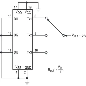
Off Source Impedance (Figure 1) Tx1 – Tx3 Zoff 300 — — Ω
Output Short–Circuit Current Tx1 – Tx3
VCC = + 5.5 V Tx1 – Tx3 shorted to GND**
Tx1 – Tx3 shorted to ± 15 V*** ISC
— —
—
— ±
60
± 100
mA
* Specifications for an ML145407 powering an ML145406 with three additional drivers/receivers.
** Specification is for one Tx output pin to be shorted at a time. Should all three driver outputs be shorted simultaneously, device power dissipation limits could be exceeded.
*** This condition could exceed package limitations.
SWITCHING CHARACTERISTICS (VCC = + 5 V ± 10%; C1, C2, C3, C4 = 10 µF; TA = – 40 to + 85°C; See Figures 2 and 3)
Characteristic Symbol Min Typ Max Unit
Drivers
Propagation Delay Time Tx1 – Tx3
Low–to–High
RL = 3 kΩ, CL = 50 pF or 2500 pF
tPLH
— 0.5 1
µs
High–to–Low
RL = 3 kΩ, CL = 50 pF or 2500 pF tPHL — 0.5 1
Output Slew Rate Tx1 – Tx3
Minimum Load: RL = 7 kΩ, CL = 0 pF
SR
— 9.0 ±30
V/µs
Maximum Load: RL = 3 kΩ, CL = 2500 pF 4.0 — —
Receivers (CL = 50 pF)
Propagation Delay Time DO1 – DO3
Low–to–High tPLH — — 1 µ
s
High–to–Low tPHL — — 1
Output Rise Time DO1 – DO3 tr — 250 400 ns
www.lansdale.com
Page 5 of 8
Issue A
PIN D
E
SCRIPTIONS
VCC
Digital Power Supply (Pin 19)
The digital supply pin, which is connected to the logic
pow-er supply. This pin should have a 0.33 µF capacitor to ground.
GND
Ground (Pin 2)
Ground return pin is typically connected to the signal ground
pin of the EIA–232–E connector (Pin 7) as well as to the logic
power supply ground.
VDD
Positive Power Supply (Pin 17)
This is the positive output of the on–chip voltage doubler and
the positive power supply input of the driver/receiver sections of
the device. This pin requires an external storage capacitor to
fil-ter the 50% duty cycle voltage generated by the charge pump.
VSS
Negative Power Supply (Pin 4)
This is the negative output of the on–chip voltage
doubler/inverter and the negative power supply input of the
driver/receiver sections of the device. This pin requires an
external storage capacitor to filter the 50% duty cycle voltage
generated by the charge pump.
C2+, C2–, C1–, C1+
Voltage Doubler and Inverter (Pins 1, 3, 18, 20)
These are the connections to the internal voltage doubler and
inverter, which generate the VDD and VSS voltages.
Rx1, Rx2, Rx3
Receive Data Input (Pins 5, 7, 9)
These are the EIA–232–E receive signal inputs. A voltage
between + 3 and + 25 V is decoded as a space and causes the
corresponding DO pin to swing to ground (0 V). A voltage
between – 3 and – 25 V is decoded as a mark, and causes the
DO pin to swing up to VCC.
DO1, DO2, DO3
Data Output (Pins 16, 14, 12)
These are the receiver digital output pins, which swing from
VCC to GND. Each output pin is capable of driving one
LSTTL input load.
DI1, DI2, DI3
Data Input (Pins 15, 13, 11)
These are the high impedance digital input pins to the
driv-ers. Input voltage levels on these pins must be between VCC
and GND.
Tx1, Tx2, Tx3
Transmit Data Output (Pins 6, 8, 10)
These are the EIA–232–E transmit signal output pins,which
swing toward VDD and VSS. A logic 1 at a DI input causes the
corresponding Tx output to swing toward VSS. A logic 0
caus-es the output to swing toward VDD. The actual levels and slew
rate achieved will depend on the output loading (RL\\CL).
Vin =±2 V 6
8
10 15
13
11
4 2
17 19
VDD VCC DI1
DI2
DI3
VSS GND Tx3 Tx2 Tx1
Rout =VinI
Figure 1. Power–Off Source Resistance
Figure 2. Switching Characteristics
Figure 3. Slew Rate Characterization DRIVERS
DI1 – DI3
3 V 0 V VOH VOL Tx1 – Tx3
tPLH tPHL
50%
tf tr
10% 90%
RECEIVERS
Rx1 – Rx3
DO1 – DO3
+ 3 V 0 V VOH VOL tPLH
tPHL
tf tr
50%
DRIVERS
Tx1 – Tx3 90%
50%
3 V – 3 V
3 V – 3 V
tSHL tSLH
SLEW RATE (SR) = – 3 V – (3 V)OR 3 V – ( – 3 V)
tSLH tSHL
E
SD CONSID
E
RATIONS
ESD protection on IC devices that have their pins accessible
to the outside world is essential. High static voltages applied to
the pins when someone touches them either directly or
indi-rectly can cause damage to gate oxides and transistor junctions
by coupling a portion of the energy from the I/O pin to the
power supply busses of the IC. This coupling will usually
occur through the internal ESD protection diodes. The key to
protecting the IC is to shunt as much of the energy to ground
as possible before it enters the IC. Figure 7 shows a technique
which will clamp the ESD voltage at approximately + 15 V
using the MMBZ15VDLT1. Any residual voltage which
appears on the supply pins is shunted to ground through the
0.1 µF capacitors.
OP
E
RATION WITH SMALL
E
R VALU
E
CHARG
E
PUMP CAPS
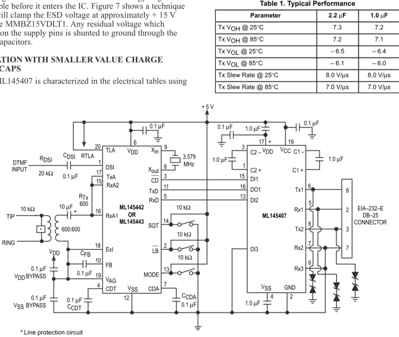
The ML145407 is characterized in the electrical tables using
10 µF charge pump caps to illustrate its capability in driving a
companion ML145406 or ML145403. If there is no
require-ment to support a second interface device and/or the charge
pump is not being used to power any other components, the
ML145407 is capable of complying with EIA–232–E and V.28
with smaller value charge pump caps.Table 1 summarizes
driv-er pdriv-erformance with both 2.2 µF and1.0µF charge pump caps.
14 600
16 TIP
13 BYPASS
DTMF INPUT
RDSI 20 kΩ
CDSI RTLA
+ 5 V
20 6 9
8 3 11 5 TLA
DSI TxA RxA2 1 17 15
VDD Xin
Xout CD TxD RxD
SQT
LB
MODE CDA VSS CDT VAG FB ExI RxA1 RTx
18 10 19 4 600:600
CFB + 10 kΩ
RING
VDD
VDD
BYPASS
VSS CCDT
12
7 2
10 kΩ
10 kΩ
10 kΩ
0.1µF
0.1µF
0.1µF
0.1µF 0.1µF
0.1µF 10µF
1.0µF 3.579
MHz
CCDA
3 1 15 16 13
17 19
6 5 8 7 9
8 2 3 7
2 4
VSS GND
DI3 DI2 DO1 DI1 C2 +
C2 – VDD VCC C1 – C1 + Tx1 Rx1 Tx2 Rx2 Rx3
* Line protection circuit
ML145442 OR
ML145443 ML145407
1.0 µF 1.0µF
1.0µF
+
EIA–232–E DB–25 CONNECTOR
0.1µF 0.1µF 0.1µF
*
Figure 4. 5 V, 300 Baud Modem with EIA–232–E Interface
Table 1. Typical Performance
Parameter 2.2 µF 1.0µF
Tx VOH @ 25°C 7.3 7.2
Tx VOH @ 85°C 7.2 7.1
Tx VOL @ 25°C – 6.5 – 6.4
Tx VOL @ 85°C – 6.1 – 6.0
Tx Slew Rate @ 25°C 8.0 V/µs 8.0 V/µs
www.lansdale.com
Page 7 of 8
Issue A
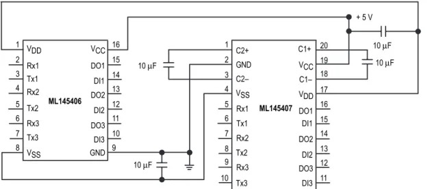
1 VDD VCC 1 C2+ C1+ 20
10 µF
ML145407 ML145406
2 3 4 5 6 7
8 9
10 11 12 13 14 15 16
2 3 4 5 6 7 8
11 12 13 14 15 16
9 10
17 18 19 Rx1
Tx1 Rx2 Tx2 Rx3 Tx3 VSS
DO1 DI1 DO2 DI2 DO3 DI3 GND
GND C2– VSS Rx1 Tx1 Rx2 Tx2 Rx3
Tx3 DI3
DO3 DI2 DO2 DI1 DO1 VDD C1– VCC
+ 5 V 10µF 10µF
10µF
Figure 5. ML145406/ML145407 5 V Only Solution for up to Six EIA–232–E Drivers and Receivers
C1+
C1–
VCC 0.1 µF
1 20
2 19
3 18
4 17
5 16
6 15
7 14
8 13
9 12
10 11
C4
C2 C2+
GND C2–
VSS VDD
0.1µF
+ 10 V + 5 V
Figure 6. Two Supply Configuration (ML145407 Generates VSS Only)
C1+
C1–
DO1 DI1 DO2 DI2 DO3 DI3
VCC 0.1 µF
1 20
2 19
3 18
4 17
5 16
6 15
7 14
8 13
TO CONNECTOR
MMBZ15VDLT × 6
9 12
10 11
C4
C2 C2+
GND C2–
Rx1 Tx1 Rx2 Tx2 Rx3 Tx3
VSS VDD
0.1 µF
C3 C1
+ 5 V
OUTLINE DIMENSIONS
P DIP 20 = RPPLASTIC DIP (ML145407RP)
CASE 738–03
1.070 0.260 0.180 0.022 0.070 0.015 0.140 15°
0.040 1.010 0.240 0.150 0.015 0.050 0.008 0.110 0°
0.020
25.66 6.10 3.81 0.39 1.27 0.21 2.80 0°
0.51 27.17
6.60 4.57 0.55 1.77 0.38 3.55 15°
1.01 0.050 BSC
0.100 BSC
0.300 BSC
1.27 BSC 2.54 BSC
7.62 BSC
INCHES MILLIMETERS DIM
A B C D E F G J K L M N
NOTES:
1. DIMENSIONING AND TOLERANCING PER ANSI Y14.5M, 1982.
2. CONTROLLING DIMENSION: INCH. 3. DIMENSION L TO CENTER OF LEAD WHEN
FORMED PARALLEL.
4. DIMENSION B DOES NOT INCLUDE MOLD FLASH.
-A-C
K N E
G F
D 20 PL
J 20 PL
L
M
-T-SEATING PLANE
1 10
20 11
0.25 (0.010) M T A M
0.25 (0.010) M T B M B
SOG 20 = -6P SOG PACKAGE
(ML145407-6P)
CASE 751D–04 NOTES:
1. DIMENSIONING AND TOLERANCING PER ANSI Y14.5M, 1982.
2. CONTROLLING DIMENSION: MILLIMETER. 3. DIMENSIONS A AND B DO NOT INCLUDE
MOLD PROTRUSION.
4. MAXIMUM MOLD PROTRUSION 0.150 (0.006) PER SIDE.
5. DIMENSION D DOES NOT INCLUDE DAMBAR PROTRUSION. ALLOWABLE DAMBAR PROTRUSION SHALL BE 0.13 (0.005) TOTAL IN EXCESS OF D DIMENSION AT MAXIMUM MATERIAL CONDITION. –A–
–B–
20
1
11
10
S
A
M
0.010 (0.25) T B S
D
20X
M
B
M
0.010 (0.25)
P
10X
J F
G
18X K
C
–T– SEATING PLANE
M
RX 45
DIM MIN MAX MIN MAX A 12.65 12.95 0.499 0.510
B 7.40 7.60 0.292 0.299
C 2.35 2.65 0.093 0.104
D 0.35 0.49 0.014 0.019
F 0.50 0.90 0.020 0.035
G 1.27 BSC 0.050 BSC
J 0.25 0.32 0.010 0.012
K 0.10 0.25 0.004 0.009
M 0 7 0 7
P 10.05 10.55 0.395 0.415
R 0.25 0.75 0.010 0.029
Lansdale Semiconductor reserves the right to make changes without further notice to any products herein to improve reliabil-ity, function or design. Lansdale does not assume any liability arising out of the application or use of any product or circuit described herein; neither does it convey any license under its patent rights nor the rights of others. “Typical” parameters which may be provided in Lansdale data sheets and/or specifications can vary in different applications, and actual performance may vary over time. All operating parameters, including “Typicals” must be validated for each customer application by the cus-tomer’s technical experts. Lansdale Semiconductor is a registered trademark of Lansdale Semiconductor, Inc.