Tampere University of Technology
A 30-dBm class-d power amplifier with On/Off logic for an integrated tri-phasing
transmitter in 28-nm CMOS
Citation
Martelius, M., Stadius, K., Lemberg, J., Roverato, E., Nieminen, T., Antonov, Y., ... Ryynanen, J. (2018). A 30-dBm class-d power amplifier with On/Off logic for an integrated tri-phasing transmitter in 28-nm CMOS. In
Proceedings of the 2018 IEEE Radio Frequency Integrated Circuits Symposium, RFIC 2018 (pp. 136-139).
[8429024] IEEE. https://doi.org/10.1109/RFIC.2018.8429024 Year
2018 Version
Peer reviewed version (post-print) Link to publication
TUTCRIS Portal (http://www.tut.fi/tutcris)
Published in
Proceedings of the 2018 IEEE Radio Frequency Integrated Circuits Symposium, RFIC 2018 DOI
10.1109/RFIC.2018.8429024
Copyright
This publication is copyrighted. You may download, display and print it for Your own personal use. Commercial use is prohibited.
Take down policy
If you believe that this document breaches copyright, please contact cris.tau@tuni.fi, and we will remove access to the work immediately and investigate your claim.
A 30-dBm Class-D Power Amplifier with On/Off Logic for an
Integrated Tri-Phasing Transmitter in 28-nm CMOS
Mikko Martelius
1, Kari Stadius
1, Jerry Lemberg
1, Enrico Roverato
1, Tero Nieminen
2,
Yury Antonov
1, Lauri Anttila
3, Mikko Valkama
3, Marko Kosunen
1, and Jussi Ryyn¨anen
1 1Department of Electronics and Nanoengineering, Aalto University, Espoo, Finland
2
Currently with CoreHW, Tampere, Finland
3
Dept. of Electronics and Communications Eng., Tampere University of Technology, Finland
mikko.martelius@aalto.fi
Abstract —This paper presents an eight-unit class-D power amplifier (PA), implemented in 28-nm CMOS. The PA is designed to utilize tri-phasing modulation, which combines coarse-amplitude polar modulation with fine-resolution outphasing components. This new technique enables achieving the back-off efficiency of multilevel outphasing without linearity-degrading discontinuities in the output waveform. Each PA unit contains a cascoded output stage with a 3.6-V supply voltage, and on/off logic enabling multilevel operation controlled by low-voltage signals. The PA achieves a peak output power of 29.7 dBm with a 34.7% efficiency, and is verified to operate with aggregated LTE signals at bandwidths up to 60 MHz at 1.7-GHz carrier frequency.
Index Terms —CMOS integrated circuits, outphasing, power amplifiers, radio transmitters, tri-phasing
I. INTRODUCTION
One of the fundamental challenges in designing radio transmitters and their power amplifiers (PA) is achieving high power efficiency without compromising linearity. This goal, in conjunction with the development towards increasingly digital-intensive circuit solutions, favors utilizing highly efficient, nonlinear switch-mode PAs. With such PAs, amplitude modulation requires discarding the conventional Cartesian transmitter structure in favor of alternative architectures. One of these architectures is outphasing, which produces amplitude modulation by altering the phase offset between two constant-envelope signal components. While enabling the use of efficient nonlinear PAs, outphasing transmitters nonetheless suffer from declining efficiency in power back-off.
Previously, improved back-off efficiency has been achieved with multilevel outphasing, in which the output amplitude is modulated by both a phase offset and discrete amplitude levels [1]. However, we have observed that amplitude-level transitions in multilevel outphasing cause inherent discontinuities in the output waveform, degrading the transmitter linearity. In order to eliminate this degradation while retaining the efficiency improvement, we have developed a new transmitter architecture
S1
–S2
S0
–S0
A1
A2
A3
A4
PA1
Outphasing Combiner
(PCB)
PA2
PA3
PA4
PA5
PA6
PA7
PA8
Polar
50 Ω
(a) (b)
Fig. 1. (a) Block diagram of the designed tri-phasing PA system. (b) Vector illustration of the tri-phasing concept.
called tri-phasing. By combining coarse-amplitude polar modulation with fine-resolution outphasing components, tri-phasing achieves the back-off efficiency of multilevel outphasing without discontinuities at amplitude-level transitions. Thus, the new architecture merges the advantages of outphasing and multilevel outphasing, particularly high linearity and back-off efficiency.
This paper presents a class-D PA implemented in 28-nm CMOS, designed to operate as part of a tri-phasing transmitter. In addition to being the first tri-phasing PA, our circuit also contains the first measured implementation of the on/off logic concept introduced in [2]. The PA achieves a peak output power of 29.7 dBm with an efficiency of 34.7% at 1.77 GHz, and is verified to operate at a 60-MHz modulated signal bandwidth. The paper is organized as follows: Section II presents the concept of tri-phasing and the PA-system structure. Section III describes the PA design in detail, followed by measurement results in
Section IV. Section V concludes the paper. II. TRI-PHASINGPA SYSTEM
This section introduces the concept of tri-phasing, a technique to achieve the back-off efficiency of multilevel outphasing with superior linearity. The block diagram of our tri-phasing PA system is depicted in Fig. 1(a). All eight class-D PA units are integrated on a single chip, and the power combiner is implemented with coupled transmission lines on PCB. The PA units are divided into polar and outphasing sections consisting of three and one PA pairs, respectively. The polar section provides coarse amplitude modulation by altering the number of active PA pairs. The constantly active outphasing PA pair enables fine amplitude resolution between polar steps by varying the phase difference between input signals S1 and S2.
Due to the voltage-subtracting characteristic of the power combiner, one input signal in each PA pair is inverted. The signal construction in tri-phasing is illustrated with vectors in Fig. 1(b).
The phase-modulated tri-phasing signal components are S0(t) = cos(ωt+φ(t)) (1)
S1(t) = cos(ωt+φ(t) +θ(t)) (2)
S2(t) = cos(ωt+φ(t)−θ(t)), (3)
whereω is the angular carrier frequency,φ(t)is the polar phase, andθ(t)is the outphasing angle. When the number of active polar PA pairs isAp(t), the output signal is
Sout(t) = 2Ap(t)S0(t) +S1(t) +S2(t). (4)
By substituting (1), (2) and (3), we obtain
Sout(t) = 2[Ap(t) + cos(θ(t))] cos(ωt+φ(t)). (5) As shown by (5), the phase modulation is defined by the polar phase, while the amplitude modulation is a combination of coarse polar and fine outphasing elements. When a coarse amplitude level is crossed, one polar PA pair is switched on or off, and the outphasing angle instantaneously shifts from 0◦to 90◦or vice versa. Ideally, this leads to smooth transitions with no abrupt change in waveform even when harmonic components are present, unlike in multilevel outphasing. The number of active PA pairs at any given output amplitude is equal between the two architectures, ideally leading to equal efficiency.
III. PA-UNITDESIGN
In this section, we describe the design details of the PA unit, shown as a schematic in Fig. 2. The output stage has a cascoded class-D structure implemented with 1.8-V thick-oxide transistors. Thus, the output voltage is always divided between two transistors, which enables using a
2.7 V
0.9 V S
A
1
1.8 V
3.6 V 1.0 V
1.0 V
NAND /NOR NAND /NOR
MODE XOR2
XOR1
OUT
M1
M2
M3
M4 DRV
DRV
Fig. 2. Simplified schematic of the PA unit.
XOR1 XOR2 A
NAND OUT S
MODE = 0
(a)
XOR1 XOR2 A
NOR OUT S
MODE = 1
(b)
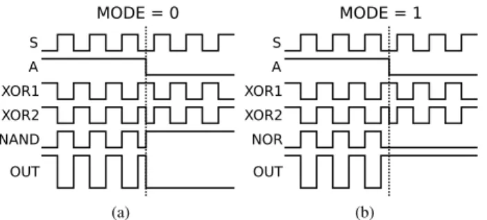
Fig. 3. Waveforms illustrating the on/off logic operation when the NAND/NOR gates are in (a) NAND mode; (b) NOR mode.
supply voltage of 3.6 V. Switch-mode operation requires the gate voltages ofM1andM4to swing between 0–1.8 V
and 1.8–3.6 V, respectively. Such voltages are provided by the driver stages (DRV), each of which consists of four inverters with increasing transistor sizes. Because the PA is designed to operate with input signals generated in the 1.0-V supply domain, DC-block capacitors and resistors are employed for biasing. The 0.9-V and 2.7-V bias voltages are generated by on-chip inverters with feedback resistors, not included in the schematic.
In order to operate as an integrated part of a tri-phasing transmitter, each PA unit is required to switch its output on and off during transmission according to the 1.0-V domain signalA. For this purpose, the circuit includes on/off logic developed from the concept presented in [2]. This solution enables generating the output-stage gate voltages in both on and off states in a manner that allows constant bias voltages and quick switching between the states. In the presented implementation, the on/off logic consists of two XOR gates in 1.0-V domain and NAND/NOR gates in 0–1.8-V and 1.8–3.6-V domains. The NAND/NOR gates of each PA unit can be individually configured to operate as NAND or NOR gates by a single control bit (MODE). The operation principle of the on/off logic is illustrated by example waveforms in Fig. 3. The input signals of the two XOR gates are a phase-modulated rail-to-rail RF signal S, a constant logical one, and an amplitude bitA.
IN1 IN2 IN1 IN2
NAND AND NOR OR IN1
IN2
IN1d IN2d
NAND AND NOR
OR
MODE MODE IN1d
IN1d IN2d IN2d
Fig. 4. Schematic of the NAND/NOR gate.
The XOR gates produce equally delayed output signals that are identical to each other whenA= 1 and inverse when A = 0. These two signals, after biasing with DC-block capacitors and resistors, are fed into NAND/NOR gates. In the case of identical inputs, the NAND/NOR gates reproduce the signal at the output. With inverse signals, the outputs of these blocks are constant, and thus the output stage is switched off. The control bit MODE defines whether the PA-unit output voltage is high or low in the off state. This flexibility enables optimal spectral performance with both voltage-adding and subtracting power combiners [3].
The schematic of the NAND/NOR gate is presented in Fig. 4. The primary design goal is to minimize timing differences between the two operation modes and thus optimize linearity when the modes are different between PA units. The input signals are fed into NAND and NOR gates, whose outputs are also inverted. In addition, chains of four inverters are employed to approximate the delay of the aforementioned gates. In the on state, when IN1d and IN2d are identical, the core circuit on the right side of Fig. 4 operates as an inverter. In the off state, when IN1d is the inverse of IN2d, the AND and NOR signals are low, and the NAND and OR signals are high. Thus, the output voltage is defined by MODE, which chooses whether all NMOS or PMOS transistors on the right side of the core conduct. As a result, the circuit as a whole operates as a NAND gate when MODE is zero and as a NOR gate when MODE is one.
IV. EXPERIMENTALRESULTS
The presented PA was implemented in 28-nm CMOS. The die micrograph is shown in Fig. 5. The eight PA units are located near the top edge, and each of their outputs is connected to two bonding pads, which are wire-bonded to the power combiner on PCB. 12 digitally controlled delay lines for static fine-tuning of the signal timing are also visible. The remainder of the depicted area is mostly occupied by supply capacitors and routing of supply and
1.42 mm
0.92 mm
Output stages Drivers + on/off
Supply capacitors + delay tuning
Fig. 5. Die micrograph of the PA.
5 10 15 20 25 30
Output power (dBm) 0
5 10 15 20 25 30 35
PA efficiency (%)
Tri-phasing Outphasing
(a)
0 15 30 45 60 75 90 Outphasing angle (deg) 0
0.2 0.4 0.6 0.8 1
Output power (W)
(b)
Fig. 6. CW measurement results at 1.7 GHz: (a) efficiency as a function of output power; (b) output power as a function of outphasing angle.
ground nodes. The depicted die area, excluding pads, is 1.31 mm2, of which the PA units occupy 0.44 mm2.
In all measurements, the PA input signals were produced by phase modulators resembling the design reported in [4]. Presented efficiency figures include all power consumption in the 1.8-V and 3.6-V supply domains. The power consumption in the shared 1.0-V supply is dominated by additional circuitry and is thus excluded from the PA efficiency. The output power is measured at the combiner output without de-embedding the combiner loss. The MODE bits of all PA units are set to zero.
Continuous-wave (CW) measurement results at 1.7 GHz are depicted in Fig. 6. The maximum output power achievable by the PA is 29.7 dBm (0.93 W) at 1.77 GHz, with an efficiency of 34.7%. In tri-phasing mode at 1.7 GHz, the peak power is reduced to 29.4 dBm (0.87 W) by the power-combiner frequency response and duty-cycle mismatches caused by the modulators. The PA efficiency is depicted as a function of output power in Fig. 6(a), demonstrating the efficiency improvement of tri-phasing compared to outphasing.
Fig. 6(b) presents the CW output power as a function of the outphasing angle at all four coarse amplitude levels. These results show that there are no gaps in achievable
1.64 1.66 1.68 1.7 1.72 1.74 1.76 Frequency (GHz) -40
-30 -20 -10 0 10 20
Power density (dBm/MHz)
BW = 20 MHz, ACLR = -37.6 dBc
(a)
1.64 1.66 1.68 1.7 1.72 1.74 1.76
Frequency (GHz)
-40 -30 -20 -10 0 10 20
Power density (dBm/MHz)
BW = 60 MHz, ACLR = -32.5 dBc
(b)
Fig. 7. Measured spectra with (a) 20-MHz LTE and (b) 60-MHz aggregated LTE signals.
TABLE I
COMPARISON OF MEASUREMENT RESULTS. JSSC JSSC ESSCIRC This
[5] [6] [7] work CMOS tech. (nm) 32 45 45 28
PA class Class D Class D Class E Class D PeakPout (dBm) 25.3 31.5 31.6 29.7
Peak efficiency (%) 35 27 43.7 34.7 Carrier freq. (GHz) 2.4 2.4 2.4 1.7
64-QAM signal WiFi WiFi LTE LTE Mod.Pout (dBm)1 19.6 24.8 26.6 23.1
Mod. efficiency (%)1 21.8 16 20.1 15.3 Max. BW (MHz) 20 20 20 60 1Bandwidth = 20 MHz
levels of output power due to the slight overlap in the output power ranges of any two adjacent amplitude levels. The maximum outphasing-angle range corresponding to the overlap is 13◦. This is significantly smaller than the similar redundancy in multilevel outphasing, where an outphasing angle of 90◦ always corresponds to a zero output power. Thus, in addition to previously mentioned advantages over multilevel outphasing, tri-phasing also features an increased effective output-amplitude resolution. The modulation performance of the PA was evaluated with 20-MHz LTE and 60-MHz aggregated LTE signals at a carrier frequency of 1.7 GHz. Signal component separation was performed according to measured minimum and maximum CW output power at each coarse amplitude level, but otherwise no predistortion was used. Fig. 7 depicts the resulting spectra, where the peak-to-average power ratio (PAPR) is limited such that the EVM of each carrier is at most 8%. With a 20-MHz bandwidth, the PA achieves an average output power of 23.1 dBm with an efficiency of 15.3% and an ACLR of -37.6 dBc. With a 60-MHz bandwidth, the average output power is 22.4 dBm, the efficiency is 13.8%, and the ACLR is -32.5 dBc.
Table I summarizes the results and compares them to previously published CMOS PAs that use outphasing or related techniques and integrate all PA units on a single die.
Among the compared PAs, our implementation features the widest reported signal bandwidth.
V. CONCLUSION
In this paper, we have presented the first reported tri-phasing PA, implemented in 28-nm CMOS. We introduced tri-phasing, a new transmitter architecture capable of achieving the back-off efficiency of multilevel outphasing without linearity degradation caused by waveform discontinuities at amplitude transitions. The presented PA contains eight units with cascoded class-D output stages, and features on/off logic circuitry that enables multilevel operation with input signals produced by low supply-voltage phase modulators. The measured peak output power at 1.77 GHz is 29.7 dBm with an efficiency of 34.7%. Operation with modulated signals has been verified at bandwidths up to 60 MHz, which is the widest reported bandwidth among similar PAs.
ACKNOWLEDGMENT
This work is supported by Nokia, the Finnish Funding Agency for Technology and Innovation, and the Academy of Finland under grants #297897 and #301820. This project has received funding from the European Union’s Horizon 2020 research and innovation programme under the Marie Sklodowska-Curie grant agreement No 704947.
REFERENCES
[1] K.-Y. Jheng, Y.-C. Chen, and A.-Y. Wu, “Multilevel LINC system designs for power efficiency enhancement of transmitters,” IEEE J. Sel. Topics Signal Process., vol. 3, no. 3, pp. 523–532, June 2009.
[2] M. Martelius et al., “Class D CMOS power amplifier with on/off logic for a multilevel outphasing transmitter,” inIEEE Int. Symp. Circuits and Systems (ISCAS), May 2016, pp. 710–713.
[3] ——, “Spectral effects of discrete-time amplitude levels in digital-intensive wideband radio transmitters,” inIEEE Int. Symp. Circuits and Systems (ISCAS), May 2018.
[4] M. Kosunenet al., “A 0.35-to-2.6GHz multilevel outphasing transmitter with a digital interpolating phase modulator enabling up to 400MHz instantaneous bandwidth,” inIEEE Int. Solid-State Circuits Conf. (ISSCC), Feb 2017, pp. 224–225.
[5] H. Xu, Y. Palaskas, A. Ravi, M. Sajadieh, M. A. El-Tanani, and K. Soumyanath, “A flip-chip-packaged 25.3 dBm class-D outphasing power amplifier in 32 nm CMOS for WLAN application,”IEEE J. Solid-State Circuits, vol. 46, no. 7, pp. 1596–1605, July 2011.
[6] W. Taiet al., “A transformer-combined 31.5 dBm outphasing power amplifier in 45 nm LP CMOS with dynamic power control for back-off power efficiency enhancement,” IEEE J. Solid-State Circuits, vol. 47, no. 7, pp. 1646–1658, July 2012.
[7] A. Banerjee, L. Ding, and R. Hezar, “High efficiency multi-mode outphasing RF power amplifier in 45nm CMOS,” in41st Eur. Solid-State Circuits Conf. (ESSCIRC), Sept 2015, pp. 168–171.