Abstract— This paper aims to model the static behavior of two generations of Silicon carbide Metal Oxide Semiconductor Field Effect Transistors (SiC-MOSFETs) subjected to temperature and input voltage variations. The description of the studied device, its electro-thermal characterizations and the comparison of two generations of SiC-MOSFETs are presented. The SPICE model provided by the constructor is studied. The comparison between the simulation results of the SPICE model and measurements reveals limitations in terms of temperature behavior and electrical effects. In order to overcome these limitations, a compact model is used. This model accurately describes the static behavior of two generations of SiC-MOSFETs. The threshold voltage extracted from the compact model is exploited to analyze the physical behavior and to compare the performance of two generations of SiC-MOSFETs.
Index Terms—SiC-MOSFET; Model; Static behavior, Electro-thermal, Physical behavior.
I. INTRODUCTION
ide bandgap semiconductors, such as Silicon Carbide (SiC) and Nitrite Gallium (GaN), show superior material properties enabling potential power device operation at higher temperatures, voltages, and switching speeds than current Silicon technology, thanks to its wide energy band gap and its higher thermal conductor [1-4]. As a result, SiC metal oxide semiconductor field effect transistors (MOSFETs) offer a way to extend the microelectronic revolution into high temperature and high power applications. The use of these new power semiconductor devices will allow improvement of the performance of power converters, which leads to an increase in the efficiency and a better use of the electric energy [5-6]. However, studies of SiC MOSFET reliability raised significant concerns on the long term operation of these devices, particularly at high temperatures [7-8]. Recently,
W. Jouha is with the Laboratory of Information Technology and Communication, National School of Applied Sciences of Tangier. University Abdelmalek Essaadi Tétouan, Maroc, and he is with Normandie Université, UNIROUEN, INSA Rouen, CNRS, Groupe de Physique des Matériaux, UMR 6634, Avenue de l’université B.P 12, 76800, France ([email protected]).
A. El Oualkadi is with the Laboratory of Information Technology and Communication, National School of Applied Sciences of Tangier. University Abdelmalek Essaadi Tétouan, Maroc ([email protected]).
P. Dherbécourt, E. Joubert and M. Masmoudi are with Normandie Université, UNIROUEN, INSA Rouen, CNRS, Groupe de Physique des Matériaux, UMR 6634, Avenue de l’université B.P 12, 76800, France ([email protected], [email protected],
numerous efforts have been dedicated to develop MOSFET models that are able to precisely describe the static behavior of power transistors, taking into account the specificities of the SiC material and the evolution of electrical parameters under temperature variations. There are two mains models type of SiC MOSFET often used in the literature. The first model is sub-circuit model [9-10]. This model uses a circuit to describe the static behavior of the SiC MOSFET, by adding electronic elements (resistances, diode and capacitances) in order to take into account some physical effects on the transistor operation. The second model is the compact model [11-13]. This model is based on physical equations and it calculates the currents from the voltages applied to the component terminals, and from the physical parameters.
This paper proposes to explore the electro-thermal static behavior and understand the physical parameters variations of power SiC-MOSFETs. In the first time, the SPICE model developed by the CREE constructor has been studied [14], the simulation results based on this model under LTSpice are compared to measurements. Thereafter, a compact model is described and used in order to improve the limits of SPICE model. The threshold voltage extracted from this compact model will be exploited to analyze the static behavior of the transistor, and compare the performance of two generations of SiC-MOSFETs.
This paper is organized as follows. Section II presents the studied devices, their structures and the electro-thermal characterization. Section III describes the SPICE model. Section IV develops the compact model based on physical equation and presents the analysis of the threshold voltage according to the temperature. Finally, the conclusion is given in section V.
II. DESCRIPTION AND ELECTRO-THERMAL CHARACTERIZATION OF STUDIED DEVICES
A. Description of the SiC-MOSFETs
The high power SiC-MOSFETs from the CREE Company have been chosen for this study. The second generation of the SiC-MOSFET G2 (10A, 1200V) referenced “C2M0280120D” is compared to the third generation G3 (11A, 900V) referenced “C3M0280090D” [15-16]. The choice of these two generations is based on the fact that both references have approximately similar nominal drain currents. Figure 1 shows the physical structures of the two generations. The devices are n-channel vertical D-MOSFETs (double-diffused MOS) with
An Improved SPICE Model for the Study of
Electro-thermal Static Behavior for two New
Generations of SiC MOSFET
W Jouha, P Dherbécourt, A El Oualkadi, Member, IEEE, Eric Joubert and M Masmoudi
http://innove.org/ijist/ 21 SiC substrate. The constructor maintains the same planar
structure for the two generations of MOSFETs. However, the doping is optimized for the third generation. Moreover, the pitch is reduced as well as the epitaxy thickness, and the gate width. These improvements increase the maximum operating temperatures which reduce the size of the cooling devices required in energy conversion systems.
B. Electro-Thermal Characterization
From each generation, a sample transistor is selected to be characterized. For this purpose, the static I-V characterizations have been performed using a bench generating a pulse measurement duration not exceeding 7 μs in order to limit the self-heating of the device under test. The measurements are conducted over a temperature range from 0°C to 135°C. The temperature is controlled by a Peltier module.
The input characteristics (Ids = f (Vgs)) and the output characteristics (Ids = f (Vds)) are measured for both MOSFET generations for various values of Vds and Vgs respectively. Figure 2 shows the input characteristics, while Figure 3 shows the output characteristics.
These electro-thermal characterizations allow the extraction of the MOSFET electrical parameters: the transconductance gm and the on-state resistance Rds(on). These parameters are used to study the behavior of the transistor as a function of temperature and compare the two generations transistors. The transconductance gm represents the image of the effective electron mobility in the channel according to the following equation [18]:
Ncell.Z .Cox n.µ
gm Vds
Lch =
(1)
Where, Ncell is the number of transistor cells, Z is the
length of a cell, Cox is the gate oxide capacitance and Lch is the channel length. The transconductance is calculated from the input characteristics gm = (Ids/Vgs). Figure 4 shows the transconductance as a function of the input voltage Vgs for various temperatures.
For both generations, the transconductance gm rises with the increase of the temperature and the input voltage Vgs, up to a critical voltage Vgs where gm decreases with the increasing temperature. This critical point is named “Zero Temperature Coefficient” (ZTC). It is related to the dependence of the electron mobility to the temperature and the transversal electric field generated by the input voltage Vgs [19]. The ZTC point appears at Vgs = 9V for the third generation before that (a)
(b)
Fig. 1. MOSFET structure: (a) second generation (G2), and (b) third generation (G3) [17].
Fig. 2. Input characteristics for Vds=18V, at three temperatures (25°C,
80°C and 135°C) for two generations G2 (solid) and G3 (dashed).
(a)
(b)
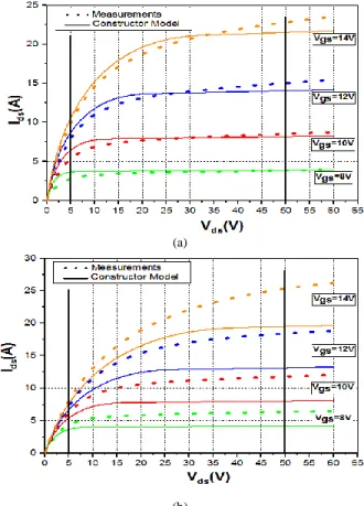
Fig. 3. Output characteristics for Vgs (8V, 10V, 12V and 14V), and for
of the second generation which appears at Vgs = 10V. This can be justified by the low threshold voltage, extracted from datasheet, for the third generation.
Considering the output characteristics, the definition of the on-state resistance Rds(on) is necessary to identify the power losses of the MOSFET in conduction. This resistance represents the variation of output voltage Vds divided by the output current Ids (Rds(on) = (Vds/Ids)). The Rds(on) is calculated for Ids = 5A and Vgs = 14V for various temperature values between 0°C and 135°C. Figure 5 shows the Rds(on) as a function of temperature for the two generations.
The two generations have the same behavior of Rds(on) as a function of temperature. The Rds(on) rises with the increase of temperature [20-21]. However, the Rds(on) value for the third generation is less than that of the second generation. This is due to the size reduction of oxide thickness and gate width of the third generation structure.
III. SPICE MODEL OF SIC-MOSFET
The constructor provides a SPICE model for his transistors. The simulation of this model is performed under LTSpice tool. Figures 6 and 7 show the comparisons of the output characteristics between the simulation results of SPICE model and measurements for two generations of SiC-MOSFET. However, Tables I and II show the relative variations between the SPICE model and measurements for the two generations of SiC-MOSFET at two values of Vds (5V and 50V). The
(a)
(b)
Fig. 6. The comparison of the output characteristics between the simulation results of SPICE model and measurements of the second generation of SiC-MOSFET at two temperatures: (a) 25°C, and (b) 135°C.
(a)
(b)
Fig. 7. Comparison of the output characteristics between the simulation results of SPICE model and measurements of the third generation of SiC-MOSFET at two temperatures: (a) 25°C, and (b) 135°C. Fig. 4. Transconductance gm as a function of Vgs at three temperatures
(25°C, 80°C and 135°C) for two generations G2 (solid) and G3 (dashed).
Fig. 5. On-state resistance Rds(on) as function of temperatures at Vds= 20V
http://innove.org/ijist/ 23 absence of measurements values in Table II for Vgs = 12V and
Vgs = 14V at Vds = 50V is due to the current limitation of the measuring probe (Idsmax = 28A). The relative variation of Ids is calculated by:
Ids( sim ) – Ids( mes )
Relative variation 100
Ids( sim )
=
(2)
Where, Ids(sim) is the simulation value of Ids and Ids(mes) is the measurement value of Ids.
The comparison of these results shows significant disparities between the SPICE model and the measurements. The exploitation of the SPICE model shows an insufficient dependence of the temperature effects on the static behavior of the transistor. The parameters of constructor model have fixed values and they are not taking into account the variation of the electrical and physical parameters of the transistor (threshold voltage, effective mobility of electrons) as a function of temperature and the voltages applied to its terminals (Vds and Vgs). These limitations make this model incompatible with the use of these components under operational conditions at various temperatures [21]. In fact, the SPICE model is only useful for the circuit design on the simulation tools. Hence, the need to use another model based on physical equations which can be more flexible, precise and can take into account the evolution of electrical parameters with temperature.
IV. COMPACT MODEL OF SICMOSFET
In order to overcome the limitations of the SPICE model, we use a compact model presented in [22]. This model describes the output current Ids in two operating regimes by the following equations:
• Linear regime
(
0 ≤ Vds ≤ Vgs−Vth 𝑃𝑣𝑓 ):2 ) gs (V 1 ) ( ) (
1
− − − − − − + = y y th V y ds V y vf P ds V th V gs V th V gs V p K f K ds I (3)
•
Saturationregime(0 ≤Vgs−Vth Pvf ≤ Vds):
2 Kp(Vgs Vth)
Ids ( 1 Vds)
2( 1 (Vgs Vth)) −
= +
+ − (4)
Where, Kp is the saturation region transconductance expressed in (A/V2). The parameter θ is an empirical correction factor (V-1) introduced to take into account the mobility reduction. Pvf and Kf are two correction factors for the pinch voltage and the Kp respectively, λ is the coefficient of the channel modulation effect, and y is an exponent. The extraction of the model parameters is based on the use of static measurements I-V in pulsed mode with the Levenberg-Marquardt optimization algorithm [23-24].
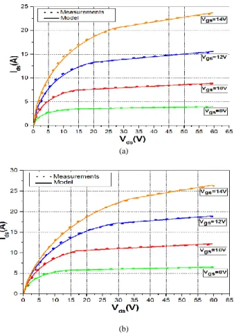
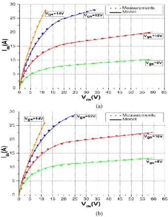
The compact model has been exploited to describe the static behavior of two generations of SiC MOSFET according to the temperature. Figures 8 and 9 show the output curves of the compact model compared to measurements for two generations of SiC MOSFET. Tables III and IV show relative variations between measurements and simulation results of the compact model for the two generations.
TABLEII
RELATIVE VARIATIONS BETWEEN THE SPICE MODEL RESULTS AND MEASUREMENTS FOR THIRD GENERATION
Temperature 25°C 135°C
Vds
Vgs 5V 50V 5V 50V
8V 25.82 % 0.5 % 0.98 % 4.8 % 10V 13.56 % 28.01 % 3.54 % 17.78 %
12V 8.69 % - 4.24 % -
14V 3.18 % - 7.25 % -
(a)
(b)
The results show that the compact model is more accurate and matches very well the measurements. The difference between the simulation results of the compact model and measurements is very lower compared to the obtained results using the SPICE model (Table I and Table II). The obtained results show the efficiency of the compact model on the
temperature range from 0°C to 135°C and for various values of the voltage Vgs.
One of the important parameters extracted from the compact model is the threshold voltage Vth. Figure 10 shows the evolution of threshold voltage Vth as a function of temperature for two generations of SiC MOSFET.
From Figure 10, it is observed that Vth decreases when the temperature increases for two generations of SiC MOSFET. Indeed, the increase of temperature causes the appearance of charges in the oxide and the decrease of the N channel resistance [25]. Physically, the relation between Vth and temperature is given by [18]:
ox C
ox Q ) i n
A N ln( q
j KT 2
ox C
) i n
A N ln( A N j kT sic 4
th
V = + −
(5)
Where, Cox=(3.9 ε0/ tox) is the gate oxide capacitance, ε0 and εSiC are the permittivity for the vacuum and the semi-conductor SiC respectively, tox is the oxide thickness, Qox is the total effective charge in the oxide, NA is the doping concentration of N, et ni is the intrinsic carrier concentration.
The equation 5 shows the dependence of Vth on temperature and the physical parameters of transistor particularly NA and Cox. Since the third generation has an optimized doping and a reduced oxide thickness compared to the second generation, the Vth of the third generation is reduced compared to the second generation.
V. CONCLUSION
This study aims to characterize and to model the static behavior of two generations of SiC-MOSFETs. We investigated the behavior of their relevant parameters (transconductance gm and on-state resistance Rds(on)) as a function of the temperature and the input voltage input Vgs.. The comparison between the simulation results based on constructor’s SPICE model and the measurements shows significant differences. These dispersions are justified by the limitation of SPICE model in terms of thermal and electrical constraints. A compact model based on the physical equations of the component overcomes these limitations. This model describes accurately and efficiently the static behavior of the (a)
(b)
Fig. 9. Comparison of the output characteristics between the compact model and the measurements of the third generation of SiC MOSFET at two temperatures: (a) 25 °C, and (b) 135 °C.
TABLE III
RELATIVE VARIATIONS BETWEEN THE COMPACT MODEL RESULTS AND MEASUREMENTS FOR SECOND GENERATION
Temperature 25°C 135°C
Vds
Vgs 5V 50V 5V 50V
8V 4.69 % 0 % 4.86 % 0.15 % 10V 4.09 % 1.16 % 1.77 % 0.16 % 12V 1.53 % 0.06 % 3.32 % 0.1 % 14V 0.6 % 0.13 % 3.74 % 0.43 %
TABLE IV
RELATIVE VARIATIONS BETWEEN THE COMPACT MODEL RESULTS AND MEASUREMENTS FOR THIRD GENERATION
Temperature 25°C 135°C
Vds
Vgs 5V 50V 5V 50V
8V 3.62 % 0.2 % 0.03 % 1.57 % 10V 1.69 % 0.01 % 1.18 % 0.09 %
12V 0.47 % - 4.66 % -
14V 1.03 % - 1.45 % -
Fig. 10. Threshold voltage Vth as function temperature at Vds =20 V for two
http://innove.org/ijist/ 25 technology.
ACKNOWLEDGMENT
This work is financially supported by the PHC Toubkal project (code TBK/17/41).
REFERENCES
[1] D. Nakamura, I. Gunjishima, S. Yamaguchi, T. Ito, A. Okamoto, H. Kondo, S. Onda and K. Takatori, "Ultrahigh-quality silicon carbide single crystals", Nature, Vol 430, pp 1009–1012, 2004.
[2] F. Bjork, M. Treu, J. Hilsenbeck, M. A. Kutschak, D. Domes, and R. Rupp, “1200V SiC JFET in Cascode Light Configuration: Comparison versus Si and SiC Based Switches”. Materials Science Forum, vol. 679-680, Mar. 2011.
[3] J. S. Glaser, J. J. Nasadoski, P. A. Losee, A. S. Kashyap, K. S. Matocha, J. L. Garret, L. D. Stevanovic, “Direct Comparison of Silicon and Silicon Cabride Power Transistors in High-Frequency Hard-Switched Applications”, in Applied Power Electronics Conference and Exposition, Twenty-Sixth Annual IEEE, 2012.
[4] J. Millán, P. Godignon, X. Perpiñà, A. Pérez-Tomás and J. Rebollo, "A Survey of Wide Bandgap Power Semiconductor Devices," in IEEE Transactions on Power Electronics, vol. 29, no. 5, pp. 2155-2163, 2014. [5] A.I. Maswood, P. H. Raj, P.L.A. Vu, “Efficiency of Silicon Carbide
Based Power Inverters Analytical Results”, Developments in Renewable Energy Technology (ICDRET), IEEE, 2012.
[6] V. Pala, E. V. Brunt, L. Cheng, C. J. Scozzie, “10 kV and 15 kV Silicon Carbide Power MOSFETs for Next-Generation Energy Conversion and Transmission Systems”, European Union, 2014.
[7] R. Kaplar, M. J. Marinella, S. DasGupta, M. A. Smith, S. Atcitty, M. Sun, and T. Palacios, “Characterization and reliability of SiC- and GaN based power transistors for renewable energy applications”, in Energy tech, 2012 IEEE, pp. 1–6, 2012.
[8] L. Yu, G. Dunne, K. Matocha, K. Cheung, J. Suehle, and K.Sheng, “Reliability issues of SiC MOSFETs: A technology for high temperature environments”, Device and Materials Reliability, IEEE Transactions on, vol. 10, no. 4, pp. 418–426, 2010.
[9] Y. Cui, M. Chinthavali and L. M. Tolbert, "Temperature dependent Pspice model of silicon carbide power MOSFET," 2012 Twenty-Seventh Annual IEEE Applied Power Electronics Conference and Exposition (APEC), Orlando, FL, 2012, pp. 1698-1704.
[10] J. Jang, T. Arnborg, Z. Yu, R. W. Dutton. “Circuit Model for Power LDMOS including Quasi-Saturation”, Proc. SISPAD,1999, pp.15-18. [11] J. Victory, C. C. McAndrew, R. Thoma, K. Joardar, M. Kniffin, S.
Merchant, D. Moncoqut. “A Physically-Based Compact Model for LDMOS Transistors“, Proc. SISPAD, 1998, pp. 271-274.
[12] S. Potbhare, N. Goldsman, A. Lelis, J. M. McGarrity, F. B. McLean, and D. Habersat, “A physical model of high temperature 4 H-SiC MOSFETs”, IEEE Trans. Electron Devices, vol. 55, no. 8, pp. 2029– 2039, 2008.
[13] M. Hasanuzzanman, S. K. Islam, and L. M. Tolbert, “Design, modeling and characterization of power MOSFET in 4 H-SiC for extreme environment applications”, Proc. Government Microcircuit Appl. Critical Technol. Conf., pp. 449–452, 2005.
[14] C2M0280120D constructor model: http://go.wolfspeed.com/all-models [15] Cree Inc. C2M0280120D SiC MOSFET datasheet
Congress and Exposition, IEEE, pp. 1480-1487, 2009.
[21] W. Jouha, P.Dherbecourt, E.Joubert, A. El Oualkadi, “ Static Behavior Analysis of Silicon Carbide Power MOSFET for Temperature Variations” , 2nd International Conference on Electrical and Information
Technologies ICEIT, 2016.
[22] W. Jouha, A. E. Oualkadi, P. Dherbécourt, E. Joubert and M. Masmoudi, "Silicon Carbide Power MOSFET Model: An Accurate Parameter Extraction Method Based on the Levenberg–Marquardt Algorithm," in IEEE Transactions on Power Electronics, vol. 33, no. 11, pp. 9130-9133, Nov. 2018.
[23] K . Levenberg, “A method for the solution of certain nonlinear problems in least squares”. Quart. Appl. Math. 2, 1944. 164-168.
[24] D. W. Marquardt, “An algorithm for least squares estimation of nonlinear parameters”, SIAM J. Appl. Math. 11, 1963. 431-441. [25] R. Ouaida, “Vieillissement et mécanismes de dégradation sur des