Visualizing Carrier Dynamics in Transition Metal Dichalcogenide
Nanoflakes using Femtosecond Pump-Probe Microscopy
By
Emilee Armstrong
Senior Honors Thesis
Department of Physics and Astronomy
University of North Carolina at Chapel Hill
April 24, 2019
Abstract
Transition metal dichalcogenides are a semiconducting material that are of interest in the scientific commu-nity for their applications in photovoltaics, flexible electronics, and medicine. It is important to understand how the structural features of these materials impact the carrier dynamics, such as exciton recombination and free carrier relaxation, so that their behavior in electronic applications can be better understood. Within this experiment, two transition metal dichalcogenides, molybdenum disulfide (MoS2) and tungsten disulfide
(WS2) were investigated using femtosecond pump-probe microscopy. Pump-probe microscopy enables the
measurement of dynamics that occur on fast time scales in precise regions. In the WS2 study, it was found
that excitons recombine at a faster rate at the edge of the flake in comparison to the center. The impact of nanoflake thickness on carrier dynamics in MoS2 was also explored, and it was found that thinner flakes
1
Background
Transition metal dichalcogenides (TMDCs) are a semiconducting material that have been investigated for their applications in a variety of fields, including energy harvesting and flexible electronics [7]. TMDCs are a layered 2D material with strong spin-orbit coupling. Characterizing the material properties of TMDCs is important for understanding how they can be used in these applications. In particular, the impact of structural features on the dynamics of the material can be investigated by observing the excited state dynamics [4].
Molybdenum disulfide (MoS2), molybdenum diselenide (MoSe2), tungsten disulfide (WS2), and tungsten
diselenide (WSe2) are four types of TMDCs. MoS2 is the most widely studied of these TMDCs due to its
applications and photophysics [7]. Many of these TMDCs have been studied at the nanoscale to understand their properties for small scale applications. Generating and studying TMDC nanoflakes is one method for investigating the material properties at the nanoscale. Nanoflakes are characterized by inhomogeneity, as shown by the atomic force microscopy image in Figure 1. There are regions of differing thicknesses on this nanoflake.
Figure 1: An atomic force microscopy image of a WS2 nanoflake [6]. The colorbar to the right of the
image shows the range of flake thickness. The flake has an inhomogeneous surface, necessitating precision techniques to characterize the material.
To characterize TMDC nanoflakes, a technique that is able to precisely measure the dynamics at a variety of locations on a small scale is necessary. Moreover, the excited state dynamics of TMDCs occur in time scales on the order of nano to femtoseconds [4]. One technique that enables the precise measurement of the fast dynamics in these nanoflakes is femtosecond pump-probe microscopy. Pump-probe microscopy is a technique that combines the spatial resolution of microscopy with the temporal resolution of ultrafast spectroscopy. Through localized excitation, pump-probe microscopy enables the exploration of how carrier dynamics, such as recombination and diffusion, depend on structural features. Several structural features that were investigated include the location of excitation and the thickness of the nanoflake.
Pump-probe microscopy involves a two laser pulse technique. First, a higher energy pump pulse, com-monly near the UV region of the electromagnetic spectrum, excites a precise location on the sample. A lower energy probe pulse, which is commonly near the infrared, is then used to measure the change in transparency of the sample over time. This change in transparency can be attributed to the dynamics of carriers and excitons in the sample. The probe beam can arrive simultaneously to the pump beam or be delayed with respect to it.
Excitons and free carriers contribute to the dynamics seen in TMDC nanoflakes [4]. Both are formed when the material is excited. An exciton is formed when an electron is excited to the conduction band, leaving behind a hole in the valance band. The electron and hole are a bound pair. Free carriers are also formed when electrons are promoted to the conduction band. However, the free carrier electrons are able to move independently of their holes. Exciton and free carrier dynamics are important because they are energy carriers. A band structure diagram for MoS2 is shown in Figure 2.
Figure 2: The band structure diagram of MoS2 (left) [2]. A and B demonstrate the higher energy direct
bandgap that excitons are formed over. They correlate to the A and B excitons in the sample. The X demonstrates the formation of free carriers over the lower energy indirect bandgap. The yellow box to the right shows a zoomed in image of the band structure diagram to demonstrate that the excitons are stabilized due their binding energy. The band structure diagrams of WS2, MoSe2, and WSe2 show similar
band structures.
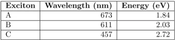
peaks, labeled A, B, and C on the diagram. The peaks are from the presence of excitons from differeing band energy levels. The signal at greater wavelengths is attributed to free carriers. When considering this transmittance graph within the context of pump-probe microscopy, the near UV pump beam is exciting the sample by the C exciton while the near infrared probe beam is measuring by the free carrier signal. This suggests that both excitons and free carriers are present in the sample.
Figure 3: A transmittance graph from a MoS2 nanoflake. This graph was generated using a
microspec-trophotometer. The A, B, and C peaks correspond to three different energy levels of excitons. The signal at higher wavelengths is from free carriers.
The wavelength and energy levels for each of the excitons are shown in Table 1.
Exciton Wavelength (nm) Energy (eV)
A 673 1.84
B 611 2.03
C 457 2.72
Table 1: Wavelength and energy values for the MoS2 transmittance graph in Figure 3
The free carriers relax to the edge of the conduction band, where they then relax through the indirect bandgap. The free carriers at the band edge render the sample metallic and cause light to scatter, resulting in a negative transparency signal. Free carriers have a much longer lifetime, typically on the order of hundreds of picoseconds, due to the indirect bandgap. The probe beam measures the change in transparency of the signal. Its arrival to the sample is delayed so that the change in transparency over time can be observed.
Through this project, the carrier dynamics of two TMDCs, MoS2and WS2, were investigated using
fem-tosecond pump-probe microscopy. The impact of their structural features on carrier behavior was explored by observing the dynamics at different excitation locations and thicknesses on the nanoflake. A goal of this experiment is to determine the carrier dynamics so that it can be understood how these materials can be used in electronic applications. To do this, an understanding of the differences between TMDC materials will also be necessary.
2
Experimental Setup
The MoS2and WS2samples were bought from 2D Semiconductors, and their samples undergo numerous
cleaning processes to eliminate defects. It is therefore hypothesized that the results seen in these experiments are due to the material properties and not defects. The MoS2 and WS2 nanoflakes are prepared using
exfoliation. A double sided piece of Scotch Tape was used to exfoliate a small piece of material from bulk material. Another piece of tape was then attached to the tape with the sample, and after pressing them together the tape pieces were pulled apart. This process was repeated 10-15 times, producing thinner and thicker nanoflakes. The tape was then pressed to a quartz substrate slide. Van der waals forces hold the nanoflakes to the substrate. To remove tape residue and other unwanted particles, the substrate slide was placed in a dish with acetone and a magnetic stirrer. This was then set on a magnetic stir plate for 20 minutes.
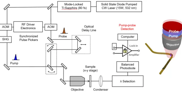
The substrate slide is then placed on the sample stage of the pump-probe microscopy setup. Figure 4 shows the setup for this experiment, and this setup will be briefly described here. First, a solid state diode pumped continuous wave laser beam is emitted with a wavelength of 850nm and a mode-locked Ti:Sapphire laser generates 80fs pulsed beams. The laser beam is split in two, and half of the beam becomes the pump and half the probe. The pump beam is generated by sending the beam through an acousto-optic modulator (AOM) and a second harmonic generator (SHG). The AOM is a pulse picker which aids in reducing the repetition rate of the laser. The SHG reduces the wavelength of the pulse from 850nm to 425nm, forming the higher energy pump beam. The pump beam is then sent to the objective, where it is focused on the sample. The pump beam is around 400nm in diameter. To prepare the probe beam, the beam is sent through an AOM like the pump beam. It is then sent through an optical delay line, which allows for the arrival of the probe beam to the sample relative to the pump beam to be adjusted. By increasing the distance the light has to travel, the pump-probe delay time is increased. The probe is then sent to the objective and is focused on the sample. The probe beam has a diameter of around 800nm. For this experiment, the pump and probe beams are spatially overlapped. The sample is placed on an x-y sample stage so that the sample can move under the beams. After the sample stage, the light goes through a filter that blocks the probe beam, followed by a balanced photodiode that measures the change in probe transmission.
Figure 4: The setup for the pump probe microscopy. The formation of the pump beam is shown on the left side of the figure while the formation of the probe beam is shown in the middle. To the right of the setup image, an example of the pump and probe beams being used to excite a nanowire is shown.
the formation of excitons in the sample. SOPP images can be generated for different pump probe delays, and the change in transparency demonstrates a change in the excited state dynamics. This will be explored further in the Results and Discussion section.
The second type of data that can be generated by ultrafast pump-probe microscopy is a transient, which is shown on the right of Figure 5. This graph shows the change in intensity (∆I), corresponding to the transparency, as a function of the pump probe delay for a particular point on the nanoflake. The setup of the pump-probe microscope allows for the delay to be changed continuously and for points to be measured throughout that process. The transient is marked by a rapid change in transparency at a delay of 0s, which marks the time when the pump beam arrives at the nanoflake. After this sharp increase, there is an exponential decay followed by a longer lived negative component. Excitons and free carriers contribute to the signal, and the specific ways in which they generate the signal will be discussed in the following section, Preliminary Research for Data Analysis.
Figure 5: Example Transient and SOPP image
University of North Carolina at Chapel Hill’s CHANL facility was used to generate transmittance data for the nanoflakes. To determine the thickness of the nanoflakes, an atomic force microscope was used. This was an Asylum Research MFP3D atomic force microscope.
3
Preliminary Research for Data Analysis
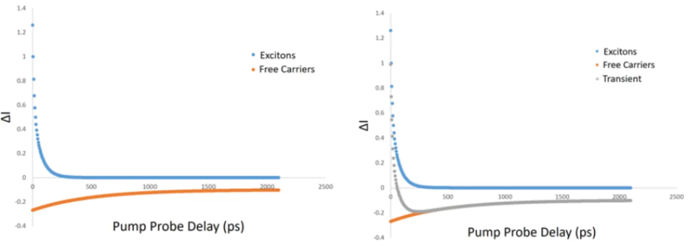
Both excitons and free carriers influence the transient signal generated from pump-probe microscopy. The contributions from these components can be modeled independently, as shown in the left graph of Figure 6. The blue dots show the fast exponential decay of the exciton signal. The long lived negative component, shown by the orange dots, is associated with free carriers, and it also decays exponentially. When these two signals are summed together they form the curve of the transient from pump-probe microscopy, as shown in the right graph of Figure 6.
Figure 6: Exciton and free carrier contributions to the transient generated from pump-probe microscopy. The left image models the decay from the excitons (blue) and the longer lived negative signal from the free carriers (orange). When added together, these signals result in the transient (gray) shown in the left image.
In order to determine which component of the transient is from excitons and which is from free carriers, a power study conducted on a WS2 nanoflake was used [6]. The WS2 nanoflake is shown in Figure 7. For
this experiment, the power of the pump beam was set at 5 picojoules per pulse (pJpp), 9pJpp, 17pJpp, and 23pJpp. The graph on the right side of Figure 7 shows that the fast initial decay is power dependent while the rate of change of the longer lived negative component is not. The power dependence of the decay suggests that the fast decay is associated with excitons. A greater beam power provides more energy per pulse, which enables excitons to be excited. Since the exciton decay rate is driven by exciton-exciton annihilation increasing the concentration of excitons increases the decay rate. The observed increase in the decay rate of the initial transient indicates that the initial decay is associated with excitons. The free carriers are predicted to be responsible for the longer lived negative component of the transient, as the decay rate of free carriers is not power dependent.
This understanding of the contribution of the excitons and free carriers to the transients will be used to evaluate the carrier dynamics of nanoflake structural features in the following section.
4
Results and Discussion
The carrier dynamics at various excitation locations was investigated in WS2 nanoflakes. The primary
Figure 7: A power study of a WS2 nanoflake [6]. Atomic force microscopy was used to generate the image
of the nanoflake on the left. The white dot on this figure demonstrates the location of excitation. The left graph is shows the power dependence of the decay. The rate of decay of the longer lived negative component does not change as a function of power.
closest to the edge, followed by points 2 and 3 which increase their proximity to the center of the flake. A transient for each of these points was generated and is shown on the right side of the figure. The graph inset zooms in on the decay, which differs between the three points. Point 1 shows the sharpest decay and point 3 shows the slowest decay. The decay of the transient is representative of the exciton recombination. Therefore, excitons are recombining at a faster rate at the edges of the flake than at the center.
Figure 8: The SOPP image (left) and transient (right) for WS2 nanoflake 1. Data was collected at three
points that differ in proximity to the nanoflake edge. For the SOPP image, the red coloring on the nanoflake corresponds to a greater transparency than blue.
Another method of observing the excitation dynamics of this first WS2 nanoflake is to look at a series
corresponds to a loss of transparency and exciton recombination, excitons are seen as recombining at a faster rate at the edge of the nanoflake than the center.
Figure 9: SOPP images for WS2 nanoflake 1. The pump probe delay is provided in the lower left corner of
each flake. Red corresponds to a greater transparency than blue.
The faster recombination of excitons at the edges of the nanoflakes can be seen in other nanoflakes. Figure 10 shows a second WS2nanoflake where a transient was collected at the edge and center of the sample. The
transient of point 1, collected at the edge of the flake, has a sharper decay than that of point 2, which was collected at the center of the flake. This trend matches that of the first WS2 nanoflake, and it is seen in
other WS2nanoflakes that were observed throughout this study.
Figure 10: The SOPP image (left) and transient (right) for WS2 nanoflake 2. Data was collected at two
points that differ in proximity to the nanoflake edge. For the SOPP image, the red coloring on the nanoflake corresponds to a greater transparency than blue.
In the process of exploring carrier dynamics at the edge and center of WS2 nanoflakes, a pattern of light
and dark regions was observed during low pump probe delays. Two examples of these patterns in nanoflakes are shown in Figure 11 with WS2 nanoflakes 2 and 3. One fringe is circled in black for each of the flakes.
Figure 11: Fringes of WS2 that appear in nanoflakes 2 and 3. A fringe is circled in black for each of the
nanoflakes. These images were collected at a 0ps pump probe delay.
the fringe patterns. The top image of the figure is a WS2nanoflake that shows the fringe pattern very clearly
[6]. These fringes run along the length of the nanoflake. The lower image shows the fringes on a MoSe2
sheet, and this image was generated by Fraser et al. using a steady state laser.
Figure 12: Images of the fringe pattern appearing in other TMDC nanoflakes. The top image shows fringes running along the length of a WS2 nanoflake from Dr. Van Goethem’s studies [6]. The lower image shows a
larger region of MoSe2 WS2 fringes example from Fraser et al. [3].
An objective of this project is compare the dynamics of different types of TMDC nanoflakes, particuarly WS2 and MoS2. This would enable an understanding of how the materials could be used in different
applications. However, before being able to compare the two materials, it is essential to determine if there are factors that would influence the comparison. One of the structural factors that would impact the dynamics is thickness. The properties of TMDCs have been found to change when comparing bulk and thin material [5]. Bulk MoS2 and WS2 have an indirect bandgap. However, as the material is reduced down
to fewer than 5 layers, it is believed that there is a switch to a direct bandgap. This would have different properties for electronic applications. Due to the potential impact of thickness on dynamics, it is necessary to explore how nanoflake thickness impacts the results seen in MoS2 and WS2.
A thickness study was conducted on MoS2nanoflakes that varied in thickness across a flake. Atomic force
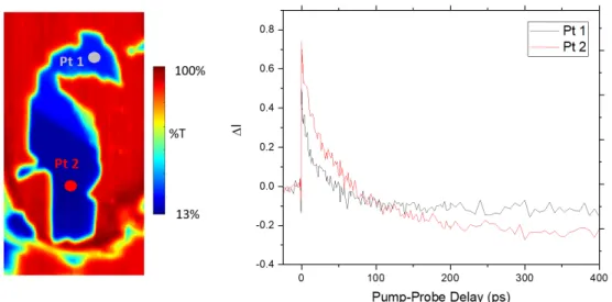
microscopy was the intended tool to determine the thickness of the nanoflakes. However, the nanoflakes are located near a marking pattern on the substrate, and this made it challenging to determine the thickness of the nanoflakes. This necessitated another way to look at the thickness of the nanoflakes. The pump transmission of the nanoflakes was therefore used to compare the relative thicknesses of regions on a nanoflake. It is hypothesized that a greater transmission would correspond to a thinner region of the flake. Figure 13 shows a transmittance graph that was generated for two points on a MoS2nanoflake. Both curves have peaks
at the same wavelength, indicating that the electronic structure of the nanoflake is not changing between these two points. However, the intensity of the transmission is different, indicating that point one transmits more light than point 2. If the hypothesis that a greater transmission corresponds to a thinner flake, point 1 is thinner than point 2.
Figure 13: A pump transmission image (left) and transmittance graph (right) for MoS2 nanoflake 1. The
transmission image shows the percent transmission of the nanoflake. Red corresponds to 100% transmission while the dark blue corresponds to 13% transmission. The transmission over a range of wavelengths was determined for two points of differing thickness on the nanoflake.
Transients were determined for the two points of differing thicknesses on MoS2 nanoflake 1. Their
transients are shown in Figure 14. Point 1 has a sharper decay than point 2, indicating that exciton recombination is occurring faster at thinner regions of the flake.
Transients were taken for another MoS2nanoflake at two points of differing thickness, as shown in Figure
15. Point 1 has a higher transmission, corresponding to a thinner section of the flake. Similarly to MoS2
nanoflake 2, the transient for point 1 has a sharper initial decay than point 2.
Five MoS2nanoflakes were investigated throughout this study. A crossing time versus transmission graph
Figure 14: A pump transmission image (left) and transient graph (right) for MoS2nanoflake 1. The
trans-mission image shows the percent transtrans-mission of the nanoflake. Red corresponds to 100% transtrans-mission while the dark blue corresponds to 13% transmission. The transient shows the change in transmission intensity over a range of pump probe delays.
Figure 15: A pump transmission image (left) and transient graph (right) for MoS2nanoflake 1. The
trans-mission image shows the percent transtrans-mission of the nanoflake. Red corresponds to 100% transtrans-mission while the dark blue corresponds to 27% transmission. The transient shows the change in transmission intensity over a range of pump probe delays for the two points indicated on the right.
that excitons recombine at a faster rate in thinner regions of nanoflakes than thicker.
Throughout this investigation of the MoS2 nanoflakes, it was observed that several of the nanoflakes had
Figure 16: Graph of the crossing time versus transmission collected for five MoS2nanoflakes. Crossing time
refers to the time at which the transient for these points crosses the x-axis. The transmission is the amount of light transmitted at these points.
Figure 17: Two MoS2 nanoflakes with thin regions are shown in the left images. The gray dots show the
5
Conclusion and Future Work
The goal of this project was to determine how structural features impact the carrier dynamics of transition metal dichalcogenide nanoflakes such as MoS2 and WS2 using femtosecond pump-probe microscopy.
Fem-tosecond pump-probe microscopy is used because it combines the spatial resolution of microscopy with the temporal resolution of spectroscopy, enabling the exploration of precise regions of the nanoflake on fast time scales. An investigation of how the location of excitation impacts the carrier dynamics was conducted in WS2. The locations of excitation were the edge and center of the nanoflake. The transient of the points at
the edge of the flake have a sharper decay than the points at the flake’s center. The steepness of the transient corresponds to the rate of exciton recombination. Therefore, the edges of the nanoflake have a faster exci-ton recombination than the center. This is something that can also be seen by observing the transmission changes in spatially overlapped pump probe images. It is hypothesized that the faster recombination rate is due to defects at the edge of the nanoflake. Understanding the carrier dynamics at different points of the material is important for the material’s applications. If WS2 is used in atomically thin electronics, the
majority of the device will be edges. It is necessary to understand the carrier dynamics at different locations so that it can be determined if these characteristics are desirable for electronic applications.
In several WS2nanoflakes, a pattern of light and dark fringes appeared in low pump probe delays. This
is a pattern that has been seen in other transition metal dichalcogenide materials, and it is hypothesized that it is due to exciton-polaritons. Exciton-polaritons are formed from semiconductor excitons and photons, both of which are present at low pump probe delays. Exciton-polaritons travel outward in a wave pattern from the location of excitation, reflect off the edge of the flake, and form an interference pattern across the flake. The fringe pattern is only seen in low pump probe delays because excitons are only present for the first hundred picoseconds after the pump arrives.
It was found that carrier dynamics also depend on the thickness of the nanoflakes. Several MoS2
nanoflakes with regions of differing thicknesses were explored. Atomic force microscopy was initially in-tended to be used to determine the thickness of the flakes. However, complications arose with the marking pattern on the substrate. Transmission was used instead to estimate the thickness of the nanoflakes. Thinner regions of flakes likely transmit more light than thicker regions, so a higher transmission was associated with a thinner region of the flake. For the MoS2 nanoflakes, it was found that thinner regions of the flake had a
steeper transient and a faster exciton recombination rate. This was further supported by graphing crossing time versus transmission.
An understanding of how structural features such as nanoflake thickness and excitation location impact the carrier dynamics is essential for comparing the use of WS2 and MoS2 in different applications. With
this understanding, the features that are seen in both types of TMDCs could be attributed to the inherent characteristics of the material rather than a result of excitation location or thickness. This knowledge could also be useful in determining how a material could be used to maximize characteristics of interest for engineers.
In the future, the thickness study for this experiment could be expanded to WS2, as MoS2 was the
material investigated in this study. It would be important to understand if thickness impacts the dynamics of MoS2 and WS2 in the same ways. Moreover, using nanoflakes that could be explored using the atomic
force microscope would enable a direct comparison between the thickness of the nanoflakes and their carrier dynamics.
Another future goal of this project would be to develop a way to fit the transients so that physical significance could be extracted from the results. Jason Malizia, a PhD candidate in the Papanikolas lab, developed a code to fit the data that accounts for the Gaussian nature of the laser beam. However, this code does not take into account how thickness and excitation location impact these dynamics. In the future, a code that took these trends into account could enable the direct comparison of different TMDC materials.
6
Acknowledgements
References
[1] Barachati, Fabio, et al. “Interacting Polariton Fluids in a Monolayer of Tungsten Disulfide.” Nature Nanotechnology, vol. 13, Aug. 2018, pp. 906–09.
[2] Dybala, F, et al. ”Pressure Coefficients for Direct Optical Transitions in MoS2, MoSe2, WS2, and WSe2
Crystals and Semiconductor to Metal Transitions.”Scientific Reports, vol. 6, 2016.
[3] Fraiser, Michael D, et al. ”Physics and Applications of Exciton-Polariton Lasers.”Nature Materials, vol. 15, 2016, pp. 1049-1052.
[4] Grumstrup, Erik M, et al. ”Pump-Probe Microscopy: Visualization and Spectroscopy of Ultrafast Dy-namics at the Nanoscale.”Chemical Physics, vol. 458, 2015, pp. 30-40.
[5] Kumar, Nardeep, et al. ”Charge carrier dynamics in bulk MoS2 crystal studied by transient absorption
microscopy.”Journal of Applied Physics, vol. 113, 2013.
[6] Van Goethem, Erika. ”Imaging Charge Carrier and Acoustic Phonon Dynamics in Semiconductor Nano-materials using Ultrafast Pump-Probe Microscopy.”Carolina Digital Repository. 2019.
[7] Vega-Mayoral, Victor, et al. ”Exciton and Charge Carrier Dynamics in Few-Layer WS2.”Nanoscale, vol.
![Figure 1: An atomic force microscopy image of a WS 2 nanoflake [6]. The colorbar to the right of the image shows the range of flake thickness](https://thumb-us.123doks.com/thumbv2/123dok_us/8331562.2210319/2.918.323.595.389.595/figure-atomic-force-microscopy-image-nanoflake-colorbar-thickness.webp)
![Figure 2: The band structure diagram of MoS 2 (left) [2]. A and B demonstrate the higher energy direct bandgap that excitons are formed over](https://thumb-us.123doks.com/thumbv2/123dok_us/8331562.2210319/3.918.267.657.129.322/figure-structure-diagram-demonstrate-higher-energy-bandgap-excitons.webp)
![Figure 7: A power study of a WS 2 nanoflake [6]. Atomic force microscopy was used to generate the image of the nanoflake on the left](https://thumb-us.123doks.com/thumbv2/123dok_us/8331562.2210319/7.918.139.769.112.401/figure-power-study-nanoflake-atomic-microscopy-generate-nanoflake.webp)