HIGH DEFORMATIONS IN LEAD SELENIDE NANOLAYERS
AND RELATED NEW PROPERTIES
A. M. Pashaev,
[a]O. I. Davarashvili,
[b]*M. I. Enukashvili,
[b]Z. G. Akhvlediani,
[b,c]L. P. Bychkova,
[b]R.G. Gulayev,
[b]M. A. Dzagania,
[b,d]and V. P. Zlomanov
[e]Keywords: nanolayers; deformations; dislocations; supercriticality; “negative” pressure.
The article deals with the modified method of “hot-wall” beam epitaxy for obtaining the strained lead selenide nanolayers over a wide range of growth rates and controlling their thickness. With detection of the two-stage growth of the layers, the layers with high deformations – tangential lattice constants, and hence with high “negative” pressure were formed. Observations of the shift of the optical spectrum in strained layers and the possibility of deep compensation of the concentration of current carriers when doping the layers with impuriti es with variable valence turned out to be interesting as well. Under high deformations, the texture of a tetragonal phase is formed. There appears a new level in the conduction band and hence additional absorption in the optical spectrum. The given specific features were first discovered in the physics and technology of IV–VI semiconductors, and they open new opportunities of using these semiconductors in IR optoelectronics.
* Corresponding Authors
E-Mail: [email protected]
[a] National Aviation Academy of Azerbaijan, Baku, Azerbaijan [b] I. Javakhishvili Tbilisi State University, Tbilisi, Georgia [c] E. Andronikashvili Institute of Physics, Tbilisi, Georgia [d] P. Melikishvili Institute of Physical & Organic Chemistry,
Tbilisi, Georgia
[e] M. V. Lomonosov Moscow State University, Moscow, Russia
Introduction
Some new data on the comprehensive research of the strained layers of IV–VI semiconductors have been presented recently.1 In bulk crystals and thick layers, the atomic number – the weight of the components of the compound determines the chain of interconnected physical properties of IV–VI semiconductors: a narrow band gap leads to small values of effective mass which, in turn, lead to high mobility of current carriers. In thin strained layers, a slight change in the distance between the atoms constituting the compound, for example, with tensile strain is accompanied by an increase in the lattice constant and the band gap, while the mobility of current carriers decreases more significantly than without relaxation of strains at the substrate-layer interface.2 As the investigation showed, it is important that, when the strained state is retained for two and more years, new opportunities to control smoothly and flexibly the properties of the nanolayers of IV– VI semiconductors and to realize innovative semiconductor device solutions are viewed.3 Hence the strained nanolayers can be classified as new nanomaterials.
Among the specific features discovered in the strained nanolayers of IV–VI semiconductors, the following ones stand out: supercritical layers under “negative” pressure, non-monotonous dependence of deformations on the growth rate for certain layer thickness, and detection of additional absorption in optical spectra.4
From the variety of methods of growing the epitaxial layers of IV–VI semiconductors from liquid and gas phases to obtain single-crystal strained layers, we chose the method of “hot-wall” beam epitaxy.5–9 In this work, the problems of the growth of the strained layers of IV-VI semiconductors and their discovered physical properties are considered and analyzed by the example of lead selenide.
Technological design and research methods
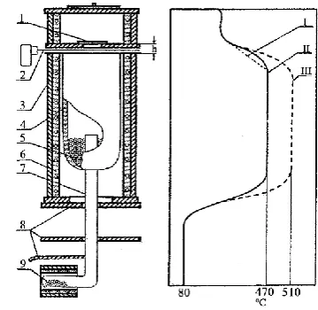
The method of “hot-wall” beam chosen for growing the strained lead selenide nanolayers is convenient for modification and control of the parameters of the layers. The schematic of the design is shown in Figure 1.
The source of epitaxy–polycrystalline lead selenide (PbSe) was placed on the bottom of a quartz ampoule 19 cm in length and 3.5 cm in diameter. The source was obtained both with the evaporation of a stoichiometric composition and small deviations from stoichiometry (within the homogeneity range) of PbSe in the evacuated system and settled in the zone at 450–510 ºС. The KCl(100), NaCl(100), and BaF2(111) substrates were prepared by cleavage off immediately before the epitaxy.
Table 1. Layer growth rate control (Tsub = 240ºC).
Variant Source temperature, ºC
Distance between ampoule edge and substrate h, mm
Layer growth rate v, nm s-1
I 470 12 0.5 – 2
II 470 1 4 – 6
III 510 1 8 – 11
The temperature in the area of the substrate placed on a stainless steel plate varied over the temperature range of 240– 310 ºС. The distance between the open edge of the quartz ampoule with the source of epitaxy and the substrate made up 1–20 mm.10 Results of layer growth rate control are shown in Table 1. Along with the source of epitaxy – PbSe polycrystals with different deviation from stoichiometry, we used an additional selenium source with heating temperature 100–120 ºС to control the type of conduction and the concentration of current carriers.
In the areas of the substrate, the source of epitaxy and the selenium reservoir, the temperature was controlled with an accuracy of 0.3 ºС. The quartz ampoule with a heater with stainless steel casing was placed in a vacuum chamber, where the pressure was kept at 2·10–6 Torr, while the realized growth rates made up 0.1–50 nm s-1. Minimal growth rates were achieved with heating of the substrate from the back side using an incandescent lamp (the temperature gradient was maintained in the thickness of the substrate) and with the distance between the open edge of the quartz ampoule and the substrate of about 20 mm.
The thickness of layers was determined by the X-ray method with the symmetric reflection of the radiation of CoKα (λ=1.7889 Å) from planes (200) and (400), and determination of the intensity-to-intensity ratio of the radiation reflected from the substrate with a deposited layer and without it. The lattice constant was determined by reflection of radiation from the plane (400) on the relation a=2λ/sinθ, where θ is Bragg’s angle.11 The concentration of current carriers and their mobility at 77 and 300 K were determined by four-probe method.12,13
Results and discussion
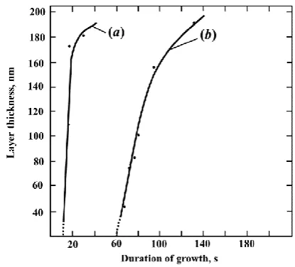
The growth rate of layers is determined by the rate of delivery of molecules to the substrate. Figure 2 shows the dependences of the thickness l of layers on the duration of their growth on KCl(100) substrates with two different distances between the substrate and the open edge of the quartz ampoule with the source I: 2.5 and 12 mm.14
Figure 2. Dependence of thickness of epitaxial PbSe layers on the duration of growth with the distance between the open edge of quartz ampoule and substrate: (a) 1–2.5mm and (b) 1–12mm.
After some time perceived as growth delay td, the layers grow faster, especially when l = 1mm. It was experimentally determined that, at 1 = 1, 2.5, 12, and 20 mm, the delay time
td was equal to 2, 9, 60, and 100 s, respectively. Taking into account the sensitivity of the X-ray method – 10 nm, the growth delay can be referred to the time of origination and merging of islets-nuclei. Attributing this event to the first stage of growth, we can conclude that the growth rate in the given cases was equal to 5, 1.1, 0.2 and 0.1 nm s-1, respectively.
At the second stage, the growth rate varies over the range from 0.6 to 50 nm s-1. At the same time, layer-by-layer growth of layers is realized with increasing elastic energy emerging due to a mismatch between the lattice constants of the layer and the substrate: аPbSe = 6.126 and аKCl = 6.290 Å. The indicators of two-stage growth of the layers of IV–VI semiconductors are described in work.15
The estimated critical thickness of layers with which elastic energy is transferred to dislocations makes up ≤2nm. As is evident from Table 2, the layers retain the strained state: the lattice constant exceeds 6.126 Å with the thickness of at least >40 nm. This is explained by braking of dislocations when their motion transfers from slip to creep in the result of the location of nonstoichiometric defects in their nuclei, or more precisely annihilation of these defects in dislocations. At the second stage of layer growth, the elastic energy of layers is expanded on the origination and acceleration of dislocations (the relaxation of strain takes place), and from the point of view of achieving maximum defects such a role of dislocations is negative. In contrast, at the first stage, the islets-nuclei flatten faster already with small layer thickness with the relaxation of the surface energy of these islets and their merging occurs, continuous growth of layers accelerates. In this case, loss and transfer of energy to dislocations by nuclei play a positive role.
Table 2. Data on conditions of growth and characteristics of strained PbSe layers on KCl(100) substrate.
For the first group of layers (SL–541, SL–558, SL–555, and SL–562) grown at l = 12 mm, temperature of the source of epitaxy 470 ºС, and the substrate 280–300 ºС (at which the migration of nonstoichiometric defects raises), low rate of growth <1.5 nm s-1, and thickness of layers <100 nm, the layers grew with high tangential lattice constants reaching 6.190 Å with deformation ~0.01. For the second group of layers (SL–215, SL–578, SL–283, and SL–284) grown at l = 2.5 mm, temperature of the source of epitaxy 470 ºС, and the substrate 300 ºС, and thickness of layers 100–200 nm, the lattice constant did not exceed 6.150 Å, and deformation was <0.003. In the third group of layers (SL–602 and SL–605) grown at l = 1mm, the temperature of the source of epitaxy 510 ºС, and the substrate 240 ºС, the lattice constant was even lower 6.140 Å with deformation <0.002, the thickness of layers was >200 nm.
It should be noted that, by its parameters, layer SL–602 can be referred both to the second and the third groups. The highest tangential lattice parameters were achieved when the substrates were heated from the back side and the distance between the ampoule with the source of epitaxy and the substrate made up 20 mm. At the temperature of the source 450 ºС and the substrate 300 ºС, the tangential lattice constant of the layer, for example, 22 nm thick reached 6.219 Å, and deformation >0.015.
Analyzing the results given in Table 2, we can infer that it is possible to achieve the maximum values of tangential lattice constant by reducing gradually the growth rate of layers, especially when the layer thickness is <100 nm. Really, as the rate of growth of layers by 0.5 nm s-1 decreases from 1.3 to 0.8 nm s-1, the tangential lattice parameter increases by 0.030 Å reaching 6.190 Å for the layer 52 nm thick. This occurs due to sufficient location of nonstoichiometric defects in dislocation nuclei. At the same time, at a certain growth rate, the minimal thickness of the layer for the maximum lattice constant can somewhat change with an increase in the density of dislocations in the substrate up to more than 106 cm–2.16,17
It is noteworthy that the increase in the tangential lattice constant is associated with tensile strain in the layers, and not with the difference between thermal expansion coefficients of
the KCl and the PbSe layers, when, on the contrary, the lattice constant of layers decreases. The increase in the lattice constant of layers is connected with the deformations formed at the substrate-layer interface, and not at the boundaries of subgrains – in this case, disorientation is minimal and makes up one hundred-thousandth of a minute.18
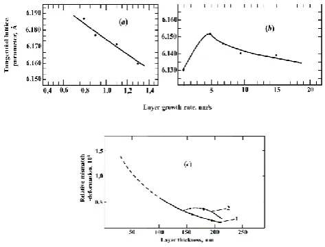
Figure 3. Dependence of tangential lattice parameter of PbSe layers on growth rate with thickness d < 100 nm (a) and d = 100–200 nm (b), and of deformation on the thickness of layers at different growth rates: 1 – 1 and 2 – 6 nm s-1 (c).
Figure 3a shows the dependence of the tangential lattice constant on the growth rate of layers for the layers <100nm thick and Figure 3b shows a similar relationship for the layers 100–200 nm thick. In the dependence of the tangential lattice constant on the growth rate, for such a layer, for example, 181 nm thick, there appears the maximum of 6.150 Å at the growth rate of 6nm/s. Apparently with a higher thickness of layers their elastic energy increases, and the relaxation of strains leads to the origination of significantly more dislocations. Bunches of dislocations are formed with their chaotic distribution, and the same number of nonstoichiometric defects is sufficient for formation of clouds limiting the displacement of dislocations. That is why braking of dislocations is more effectively than at low growth rates, when the same concentration of nonstoichiometric defects is
# Layer Temperature, °C Growth
duration, s
Layer thickness, nm
The tangential lattice constant, Å
Layer growth rate, v, nm s-1
Relative mismatch– deformation,
ε =100(аl–аPbSe)/аPbSe
Source Substrate
1 SL-541 470 300 80 101 6.162(4) 1.3 0.59
2 SL–558 470 300 77 83 6.172(0) 1.1 0.75
3 SL–555 470 300 75 68 6.177(4) 0.9 0.83
4 SL–562 470 300 67 52 6.188(2) 0.8 1.01
5 SL–215 450 240 300 200 6.129(7) 0.7 0.05
6 SL–578 470 240 30 181 6.249(0) 6.1 0.38
7 SL–283 470 240 13 110 6.144(4) 8.5 0.29
8 SL–284 470 240 15 175 6.136(7) 11.7 0.16
9 SL–602 510 240 12 206 6.139(2) 17.2 0.21
10 SL–605 510 240 20 440 6.132(6) 22.1 0.10
11 SL–623 450 300 130 25 6.202(1) 0.19 1.24
insufficient for application, but, if the density of dislocations is high the investigation of specific features of growth with the thickness of layers 100–200nm is a useful model for achieving high deformations in thinner layers.
At higher growth rates 6 nm s-1 < v < 20 nm s-1, both for the thickness of layers <100 and 100–200nm, relaxation of strains increases due to the mismatch emerging at the boundaries of subgrains (Figure 3b).4,19 These conclusions are also illustrated by Figure 3c, which shows the dependence of deformation on the thickness of layers, and that, at the layer thickness of the layer 181 nm, the deformation also increases with the increasing growth rate.
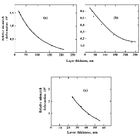
Figure 4. Layer thickness dependence of mismatch – deformation (in relation to single-crystal PbSe) in PbSe layers grown on KCl (a), BaF2 (b), and NaCl (c) substrates.
A specific role of nonstoichiometric defects with their annihilation in the nuclei of dislocations is manifested with the formation of supercritical layers as well. In Figures 4a, b, and c are shown relative mismatches – deformations in lead selenide layers growing on KCl(100), BaF2(111), and NaCl(100) substrates depending on the thickness of layers. Comparing the deformations with the thickness 20nm, in the case of KCl (а = 6.290Å), ɛ = 1.5·10–2 and, in the case of BaF2 (а = 6.200Å), ɛ = 0.6·10–2. In both cases, the deformations of ~0.001 were observed at the thickness of ~200nm. When the layers are grown on the NaCl substrate (а = 5.640Å), due to the higher mismatch in the PbSe layer 20nm thick, the deformation is higher and makes up ~2·10–2, but at the level of ~0.001 it stretches to the thickness of 60nm. In this case, the area of supercriticity reduces because of the compression of layers, while it is significantly larger with stretching – “negative” pressure.
Because of a wide range of tensile strain, it is important to study the “negative” pressure in connection with the possibility of creating a dielectric state with the shift of the impurity level with variable valence deep into the band gap. The impurities of this kind compensate electrically active nonstoichiometric defects and impurity state variables (of different sign).20
An additional resource shows up when studying the elastic properties the elastic modulus and critical deformation of PbSe, alloyed with, e.g. chrome, by the method of internal friction. It turned out that the elastic modulus of PbSe increased 3-times, the critical deformation – 2-times, and the elastic limit – 6-times.21 This allows realizing higher “negative” pressure at the same layer thickness, and hence implementing more deepening of impurity levels into the band gap with stabilization of the Fermi level and more significant compensation off the concentration of current carriers.22
Besides the double role of dislocations in the formation of strained lead selenide layers and the determination of the impact of the growth rate on the character of layer growth over a definite range of thickness, an important step is the detection of tetragonal texture in the layers.
In particular, when examining the X-ray diffraction patterns of θ–2θ scanning, it was revealed that, with the thickness of layers from 100 to 300 nm and reflection from planes (200), (400), and (600), there was detected a single band with decreasing intensity as the index h increased. With the thickness of layers less than 100nm, there appears an additional peak, and splitting of X-ray diffraction lines is observed.4,23
Figure 5. X-ray diffraction patterns of θ–2θ scanning of two PbSe layers with thickness more (SL–577) and less (SL–562) than 100 nm.
Figure 5 shows the X-ray diffraction patterns for layers SL– 578 and SL–562 with thicknesses of 181 and 52 nm, respectively. The appearance of texture in the latter case is connected with the formation of a new tetragonal phase with high deformations. The peak on the left in the angular position corresponds to a plane (002). With the increase in the level of deformation, the distance between the basic and the additional peaks increases. Such a peculiarity can be used as calibration for achieving the highest deformations, i.e., high "negative" pressure.
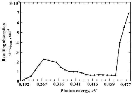
Figure 6. Resulting absorption α–αfr.car. dependence on photon
energy.
By straightening of squared absorption coefficients, more exactly of the difference between the total absorption coefficient α and the absorption coefficient for free carriers αfr.car .(α–αfr.car.), the values of lead selenide band gap determined with varying thickness of layers from 4 μm to 70nm varied from 0.286 to 0.465 eV.2,25 When the texture of the tetragonal phase appears in the X-ray spectrum, a new level emerges in the conduction band. Taking into account the effect of deformation on optical characteristics, in Figure 6 is shown the spectral dependence of α–αfr.car. at 300 K by the example of the lead selenide layer ~70 nm thick. At the concentration of current carriers in the layer of 4·1018 cm–3, additional absorption – a peak in the vicinity of 0.285 eV appears in the optical spectrum.26
The increase in the tangential lattice constant and the band gap by 0.055 Å and 0.170 eV, respectively, is an important illustration of the achievement of high deformations, i.e., supercriticity and high “negative” pressure in the layers up to ~10 kbar (with the elastic modulus of 5·1011 dyn cm-2).
Conclusion
Continuous single-crystal strained lead selenide layers 20– 500 nm thick with deformation of 0.001-0.02 were grown on the КCl, BaF2, and NaCl substrates in the "hot-wall" beam epitaxy. The detected two-stage growth of layers and non-monotonous dependence of the tangential lattice constant on the growth rate allowed us to optimize the conditions of formation of "negative" pressure in the layers and to observe a significant shift of the absorption spectra in the strained layers. Due to high deformations, the new texture of the tetragonal phase appears in the strained layers, which is accompanied by the emergence of a new level in the conduction band. The detection of additional absorption in the optical spectrum is connected with this level. By alloying with variable-valence impurities, e.g., chrome, and with the increasing elastic limit, the conditions for more significant shifting of the chrome level to the band gap and more effective compensation of the concentration of current carriers are formed. Innovative effects of the optical spectrum shift, compensation of the concentration of current carriers and detection of additional absorption will serve as a basis for designing high-temperature lasers, photodetectors and modulators of IR radiation based on the studied semiconductors.
Acknowledgment
Paper was presented at the 5th International Conference “Nanotechnologies”, November 19–22, 2018, Tbilisi, Georgia (Nano–2018).
References
1Pashaev, A. M., Davarashvili, O. I., Enukashvili, M. I., Akhvlediani,
Z. G., Bychkova, L. P., Gulyaev, R. G., Dzagania, M. A., Zlomanov, V. P., Strained semiconductor layers on dielectric substrates (for example: IV–VI materials). Preprint, 2016, Tbilisi, ISL–TSU, 22 pp.
2Pashaev, A. M., Davarashvili, O. I., Enukashvili, M. I., Akhvlediani,
Z. G., Bychkova, L. P., Gulyaev, R. G., Zlomanov. V. P., New analysis of optical parameters of the strained nanolayers of IV–VI semiconductors. Bull. Acad. Sci. Georgia, 2017, 43(3-4), 418-426.
https://doi.org/10.4028/www.scientific.net/amr.815.47 3
3Pashaev, A. M., Davarashvili, O. I., Enukashvili, M. I., Akhvlediani,
Z. G., Bychkova, L. P., Gulyaev, R. G., Dzagania, M. A., Zlomanov, V. P., Investigation of the strained nanolayers of IV–VI semiconductors on dielectric substrates. Bull. Acad. Sci.
Georgia, 2017, 43(1), 24-36.
https://doi.org/10.1088/1757-899x/503/1/012025
4Pashaev, A. M., Davarashvili, O. I., Enukashvili, M. I., Akhvlediani,
Z. G., Bychkova, L. P., Gulyaev, R. G., Dzagania, M. A., Zlomanov, V. P., Supercritical lead selenide layers at “negative” pressures. Bull. Acad. Sci. Georgia,2017, 43(2), 179-188.
https://doi.org/10.1088/1757-899x/503/1/012025
5Duh, K., Preier, H., Properties of PbS
1–xSex epilayers deposited into
PbS substrates by “hot -wall” epitaxy. J. Materi. Sci., 1975, 10, 1360-1366.
6Kasai, I., Rassett, D. W., Horhung. I., PbSe and Pb
0,8Sn0,2Te
epitaxial films on cleaved BaF2 substrates prepared by a
modified “hot-wall” technique, J. Appl. Phys., 1978, 47(7), 3167-3171. https://doi.org/10.1063/1.323111
7Lopez–Otero, A., Hot-wall epitaxy, Thin Solid Films, 1978, 49,
1-69. https://doi.org/10.1016/0040-6090(78)90309-7
8Viatkin, K. V., Shotov, A. P., Ursaki, V. V., Thin layers of PbS 1–
xSex, grown by “hot-wall” epitaxy, Inorg. Mater., 1981, 17(1),
24-27.
9Pashaev, A. M., Davarashvili, O. I., Aliyev, V. A., Gegiadze, G. G.,
Gulyaev, R. G., Enukashvili, M. I., Zlomanov, V. P., Investigation of thin epitaxial layers of lead selenide.
Georgian Chem. J., 2009, 2(3), 201-203.
https://doi.org/10.4236/jmp.2012.36068
10Pashaev, A. M. Davarashvili, O. I. Enukashvili, M. I. Akhvlediani,
Z. G. Bychkova, L. P. Dzagania, M. A. Zlomanov, V. P., Investigation of strained lead selenide nanolayers, Global J.
Eng. Sci. Res. Manag., 2016, 3(6), 56-64.
https://doi.org/10.1088/1757-899x/503/1/012025
11Pashaev, A. M., Davarashvili, O. I., Enukashvili, M. I., Bychkova,
L. P., Gulyaev, R. G., Dzagania, M. A., Lattice constant as indicator of the technology and the properties of IV–VI semiconductors, Bull. Acad. Sci. Georgia, 2017, 40(2-3), 11-16.
12Pashaev, A. Davarashvili, O. Akhvlediani, Z. Enukashvili, M.
Gulyaev, R. Zlomanov, V., Unrelaxed state in epitaxial heterostructures based on lead selenide, J. Mod. Phys., 2012, 3(6), 502-510. https://doi.org/10.4236/jmp.2012.36068
13Pashaev, A. M. Davarashvili, O. I. Akhvlediani, Z. G. Enukashvili,
M. I. Bychkova, L. P. Dzagania, M. A., Study on the forbidden gap width of strained epitaxial lead selenide layers by optical transmission, J. Materi. Sci. Eng. B, 2012, 2(2), 142-150.
14Pashaev, A. M. Davarashvili, O. I. Enukashvili, M. I. Akhvlediani,
Z. G. Gulуaev, R. G. Bychkova, L. P. Zlomanov, V. P., New studies of growth patterns of lead selenide nanolayers. Proc. Natl. Acad. Avia. Azerbaijan, 2012, 14(4), 3-8.
https://doi.org/10.4028/www.scientific.net/amr.815.47 3
15Palatnik, L. S. Sorokin, R. K. Zozulya, L. P., The mechanism of
growth of isolated particles at epitaxy of lead chalcogenides on NaCl and KCl, Solid State Phys., 1969, 11(5), 1265-1270.
16Pashaev, A. M. Davarashvili, O. I. Enukashvili, M. I. Akhvlediani,
Z. G. Gulyaev, R. G. Dzagania. M. A., Variations of the parameters of PbSe nanolayers with change of their technology. IOP Conf. Ser. Mater. Sci. Eng., 2015, 77, 012017, 2-9. https://doi.org/10.1088/1757-899x/77/1/012017
17Pashaev, A. M. Davarashvili, O. I. Enukashvili, M. I. Akhvlediani,
Z. G. Gulyaev, R. G. Dzagania, M. A., Analysis of growth and properties of epitaxial lead selenide layers in the connection of realization of high “negative” pressure. Bull. Acad. Sci. Georgia, 2012, 38(1), 31-35.
https://doi.org/10.4236/jmp.2012.36068
18Pashaev, A. M., Davarashvili, O. I., Enukashvili, M. I.,
Akhvlediani, Z. G., Gulуaev, R. G., Bychkova, L. P., Zlomanov, V. P., Stretching strain – effective “negative” pressure in lead selenide nanolayers. Int. J. Eng. & Innov. Technol., 2014, 3(11), 318-323.
https://doi.org/10.4028/www.scientific.net/amr.1025-1026.831
19Pashaev, A. M., Davarashvili, O. I., Enukashvili, M. I.,
Akhvlediani, Z. G., Gulyaev, R. G., Bychkova, L. P., Zlomanov, V. P., Modification of the properties of lead selenide layers at their nanothickness, Nano Studies, 2013, 7, 233-240.
https://doi.org/10.4028/www.scientific.net/amr.815.47 3
20Volkov, B. A., Riabova, L. I., Khokhlov, D. R., Impurities with
variable valence in the solid solutions on the base of lead telluride. Usp. Phys., 2002, 152, 1-68.
21Pashaev, A. M., Davarashvili, O. I., Aliyev, V. A., Darsavelidze,
G. Sh., Enukashvili, M. I., Zlomanov, V. P., Experimental modeling of elastic properties in epitaxial layers of IV–VI semiconductors. Trans. Natl. Acad. Avia. Azerbaijan, 2008, 5, 96-100.
22Pashaev, A. M. Davarashvili, O. I. Enukashvili, M. I. Akhvlediani,
Z. G. Gulyaev, R. G. Bychkova, L. P. Zlomanov, V. P., Modeling of quasi-dielectric state in PbSnTe and PbSnSe nanolayers with a high concentration of nonstoichiometric defects. Nano Studies, 2013, 8, 253-258. https://doi.org/10.4028/www.scientific.net/amr.815.47 3
23Pashaev, A. M. Davarashvili, O. I. Enukashvili, M. I. Gulyaev, R.
G. Dzagania, M. A. Zlomanov, V. P., On the tangential and the normal lattice constants of epitaxial lead selenide layers. Herald Azerbaijan Eng. Acad., 2011, 3(4), 13-21. https://doi.org/10.4236/jmp.2012.36068
24Pashaev, A. M., Davarashvili, O. I., Enukashvili, M. I.,
Akhvlediani, Z. G., Bychkova, L. P., Zlomanov, V. P., Study of the optical characteristics of epitaxial PbS1–xSex layers.
Global J. Eng. Sci. Res. Manag., 2016, 3(2), 46-53.
25Pashaev, A. M., Davarashvili, O. I., Enukashvili, M. I.,
Akhvlediani, Z. G., Bychkova, L. P., Zlomanov, V. P., Analysis of the absorption spectra of epitaxial lead telluride and lead selenide layers. Int. J. Eng. Inn. Technol., 2015, 4(11), 193-198. https://doi.org/10.4236/jmp.2012.36068
26Pashaev, A. M., Davarashvili, O. I., Enukashvili, M. I.,
Akhvlediani, Z. G., Bychkova, L. P., Dzagania, M. A., Zlomanov, V. P., Additional absorption in the optical spectra of the lead selenide epitaxial layers, Bull. Acad. Sci. Georgia, 2014,40(4), 285-292.
https://doi.org/10.4236/jmp.2012.36068