1 All Rights Reserved © 2017 IJDCN
VHDL Based PCM Modulator Model
Dr. Haresh Pandya
1, Mr. Mahesh Rangapariya
2, Mr. Jitendra Rajput
3ABSTRACT: The designer of an VHDL Based PCM Modulator Model has complete flexibility to select any combination of peripherals and channel. In fact, the designer can invent new, unique peripherals that can be connected directly to the processor bus. If a designer has a non-standard requirement for a peripheral set, this can be met easily with an FPGA embedded processor system. For example, a designer would not easily find an off-the-shelf processor with ten UARTs. However, in an FPGA, this configuration is very easily accomplished.
Keyword: Digital Filter, VHDL (VHSIC Hardware Description Language), FPGA (Field Programmable Gate Arrays), Electronics Switch.
Introduction
The Operation Theory of PCM Modulation
PCM modulation is a kind of source coding. The meaning of source coding is the conversion from analog signal to digital signal. After converted to digital signal, it is easy for us to process the signal such as encoding, filtering the unwanted signal and so on. Besides, the quality of digital signal is
better than analog signal. This is because the digital signal can be easily recovered by using comparator.
2 All Rights Reserved © 2017 IJDCN
Figure 9-1 Block diagram of PCM modulation.
Flat - Top Sampling
An Analogue to Digital Converter requires that the sample value be held constant for a fixed time until the conversion
is completed. This requires a flat-top sampled signal. This has approximately the same repeated frequency spectrum as with the instantaneous sampling above, but with each repetition slightly spread out.
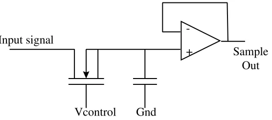
Fig 8.2 sample and hold circuit
The simplest and most common sampling method is performed by a functional block termed a Sample and Hold (S/H) circuit. The output from the circuit must be held at a constant level for the sampling duration. Control switches the MOSFET ON until the charge on C is equal to the amplitude of the sampled voltage. Control then goes LOW, the MOSFET is OFF and the charge is held by the capacitor. The charge held on the capacitor puts a voltage across the capacitor, and it is held at that value until the next time that Control switches the MOSFET ON. This is called a
sample and holds circuit and is usually used as the input to an ADC.
Fig 8.2 sample and hold signal Input signal
Vcontrol Gnd
3 All Rights Reserved © 2017 IJDCN
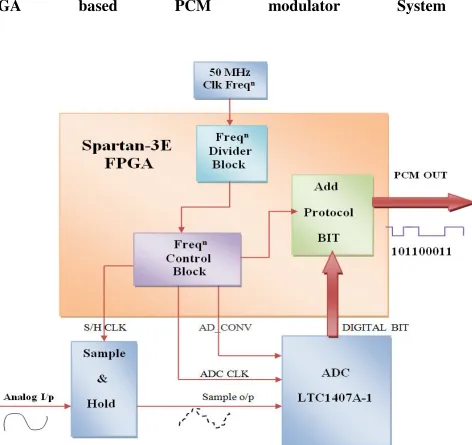
FPGA
based
PCM
modulator
System
Fig 8.3 FPGA based PCM system
Show above block diagram FPGA connect with ADC and S/H. PCM protocol generate block create inside FPGA. Analog input is connected to S/H ckt. Output of S/H connects to input of serial ADC LTC407A-1. Output of ADC LTC407A-1 connected to PCM protocol generate block of FPGA. FPGA kit has an own crystal clock generator they produce 50MHz clk frequency. Frequency control block of FPGA produce
4 All Rights Reserved © 2017 IJDCN
block is design using VHDL program. If we want PCM protocol is change using reprogramming FPGA. Finally output of protocol generates block give PCM output.
Block diagram of serial ADC
LTC1407-1
The LTCR1407-1/LTC1407A-1 are 12-bit/14-bit, 3Msps ADCs with two 1.5Msps simultaneously sampled differential inputs. The devices draw only 4.7mA from a single 3V supply and come in a tiny 10-lead MS package. A sleep shutdown feature
lowers power consumption to 10μW. The
combination of speed, low power and tiny package makes the LTC1407-1/LTC1407A-1 suitable for high speed, portable applications.
The LTC1407-1/LTC1407A-1 contains two separate differential inputs that are sampled simultaneously on the rising edge of the CONV signal. These two sampled inputs are then converted at a rate of 1.5Msps per channel.
The 80dB common mode rejection allows users to eliminate ground loops and common mode noise by measuring signals differentially from the source.
The devices convert –1.25V to 1.25V
bipolar inputs differentially. The absolute
voltage swing for CH0+, CH0–, CH1+ and
CH1– extends from ground to the supply
voltage. The serial interface sends out the two conversion results in 32 clocks for compatibility with standard serial interfaces.
Pin Configuration of
serial ADC
LTC1407-1
Pin
Function
of
serial
ADC
LTC1407-1
CH0+ (Pin 1): Noninverting Channel 0.
5 All Rights Reserved © 2017 IJDCN
respect to CH0-, with a –1.25V to 1.25V
differential swing with respect to CH0– and
a 0 to VDD absolute input range.
CH0- (Pin 2): Inverting Channel 0. CH0– operates fully differentially with respect to
CH0+, with a 1.25V to –1.25V differential
swing with respect to CH0+ and a 0 to VDD absolute input range.
VREF (Pin 3): 2.5V Internal Reference. Bypass to GND and a solid analog ground
plane with a 10μF ceramic capacitor (or
10μF tantalum in parallel with 0.1μF ceramic). Can be overdriven by an external
reference voltage ≥ 2.55V and ≤VDD.
CH1+ (Pin 4): Noninverting Channel 1.
CH1+ operates fully differentially with
respect to CH1-, with a –1.25V to 1.25V
differential swing with respect to CH1- and a
0 to VDD absolute input range.
CH1- (Pin 5): Inverting Channel 1. CH1 -operates fully differentially with respect to
CH1+, with a 1.25V to –1.25V differential
swing with respect to CH1+ and a 0 to VDD
absolute input range.
GND (Pins 6, 11): Ground and Exposed Pad. This single ground pin and the Exposed Pad must be tied directly to the solid ground plane under the part. Keep in mind that analog signal currents and digital output
signal currents flow through these
connections.
VDD (Pin 7): 3V Positive Supply. This single power pin supplies 3V to the entire chip. Bypass to GND pin and solid analog
ground plane with a 10μF ceramic capacitor
(or 10μF tantalum) in parallel with 0.1μF ceramic. Keep in mind that internal analog currents and digital output signal currents flow through this pin. Care should be taken
to place the 0.1μF bypass capacitor as close
to Pins 6 and 7 as possible.
SDO (Pin 8): Three-State Serial Data Output. Each pair of output data words represents the two analog input channels at the start of the previous conversion. The
output format is 2’s complement.
SCK (Pin 9): External Clock Input. Advances the conversion process and sequences the output data on the rising edge. One or more pulses wake from sleep.
CONV (Pin 10): Convert Start. Holds the two analog input signals and starts the conversion on the rising edge. Two pulses with SCK in fixed high or fixed low state starts nap mode. Four or more pulses with SCK in fixed high or fixed low state starts sleep mode.
6 All Rights Reserved © 2017 IJDCN
Working Flow of FPGA based PCM system
Analog signal and S/H clk both are applied to S/H block. After this process, continues analog signal is converting into discrete sample as shown in fig 8.3. Sample signal apply to ADC at a same time AD_CONV goes in high there for, ADC start conversion process. After the complete process ADC produce digital data. Get digital data in serial mode shown above fig. Output digital data is in 2’s compliment format so, converted in 1’s compliment format if require. Conversion process of data is as follow.
First fall all serial data is converting in parallel data, then logic 1 bit subtract from it. This Process converts 2’compliment to 1’s compliment data. Now, take inverse of 1’s compliment of data give final original digital data. Again parallel data convert into serial data then add protocol bit. VHDL program is use for this purpose.
VHDL program code for PCM
---
-- Company: -- Engineer:
-- Create Date: 17:03:59 09/03/2015 -- Design Name:
-- Module Name: pcm - Behavioral -- Project Name:
-- Target Devices: -- Tool versions:
-- Description: -- Dependencies: -- Revision:
-- Revision 0.01 - File Created -- Additional Comments:
---
library IEEE;
use IEEE.STD_LOGIC_1164.ALL; use IEEE.STD_LOGIC_ARITH.ALL; use IEEE.STD_LOGIC_UNSIGNED.ALL;
7 All Rights Reserved © 2017 IJDCN
---- any Xilinx primitives in this code. --library UNISIM;
--use UNISIM.VComponents.all;
entity pcm is
Port (miso,shdn,ampad,ampdo,mosi1,bclk : in STD_LOGIC;
ampcs,adcon : out STD_LOGIC_vector (1 downto 0);
clk : inout STD_LOGIC ;
DB1 : out STD_LOGIC_VECTOR(3 DOWNTO 0); dout : out STD_LOGIC_vector (13 downto 0);
ssb,daccs,ceo,initb,pcmout,RS1,rs2,RW1,rw 2,E1,e2 :out STD_LOGIC;
mosi,lmosi,ashdn,lshdn,lmiso,lampad,lampd o,aclk,lclk :out STD_LOGIC);
end pcm ;
architecture Behavioral of led is
signal dout1,smiso,pclk,E,RS,RW: STD_LOGIC;
signal cs2,cs1: STD_LOGIC_vector (1 downto 0);
signal DB:STD_LOGIC_VECTOR(3 DOWNTO 0);
signal h : STD_LOGIC_vector (7 downto 0);
signal h1 : STD_LOGIC_vector (0 to 32); signal h2 : STD_LOGIC_vector (0 to 16); signal count : integer range 0 to 2 ;
signal count1 : integer range 0 to 16 ; signal temp : integer range 0 to 4000000; signal temp1 : integer range 0 to 10:=0; signal temp2 : integer range 0 to 8:= 0; signal temp3 : integer range 0 to 33:= 0; signal temp4 : integer range 0 to 32:= 0; signal com1 : STD_LOGIC_vector (0 to 13);
signal com2 : STD_LOGIC_vector (0 to 13);
signal com3 : STD_LOGIC_vector (0 to 13);
signal lcdcnt : integer range 0 to 171; signal lcdcnt1 : integer range 0 to 121;
begin
ssb<='1'; daccs<='1'; ceo<='1' ; initb<='1'; ashdn<=shdn; lshdn<=shdn; aclk<=clk; lclk<=pclk; lampdo<=ampdo;
lampad<=ampad;
---board clock---50M--- process(bclk)
begin
if(bclk'event and bclk = '0')then
temp<= temp+1; if(temp>=2000000)then
clk<='1'; else
clk<='0' ; end if; end if ;
end process;
---pcm clock--- process(clk)
begin
if(clk'event and clk = '0')then
count<= count+1; if(count>=2)then
pclk<='1'; else
pclk<='0' ; end if; end if ;
end process;
---amp gain setting---
process(clk,ampad) begin
if(ampad='0')then
8 All Rights Reserved © 2017 IJDCN
temp1 <= temp1+1; if(temp1=10)then temp1<=0; end if; end if; case temp1 is
when 0 => cs1<= "11"; when 1 => cs1<= "11"; when 2 => cs1<= "00"; when others =>null ; end case;
ampcs<=cs1 ;
if(cs1="11")then h <= "10001000" ;
temp2<=0 ;
elsif(clk'event and clk='0')then temp2 <= temp2+1; dout1 <= h(temp2) ; if(temp2=8)then temp2<=0; end if;
end if ; end if ;
end process ;
mosi<= dout1 ; lmosi<= dout1 ;
---adc start--- process(clk,ampad) begin
if(ampad='1')then
if(clk'event and clk = '0')then temp3 <= temp3+1;
if(temp3=33)then temp3<=0;
end if; end if; end if ;
case temp3 is when 0 => cs2<= "00";
when 1 => cs2<= "11"; when 2 => cs2<= "00"; when others =>null ; end case; adcon<=cs2 ;
end process;
smiso<=miso;
lmiso<=miso;
---adc parallel out--- process (cs2,clk)
begin
if(cs2="00")then
if(clk'event and clk='0')then temp4 <= temp4+1; h1(temp4)<= smiso ; if(temp4=32)then temp4<=0; end if;
end if ; else
h2<= h1(1 to 14 )& "000" ; com1<= h1(1 to 14 ) ;
temp4<=0; end if ;
end process ;
---pcm out--- process (pclk)
begin
if(pclk'event and pclk='0')then count1 <= count1+1; pcmout <= h2(count1) ; if(count1=16)then count1<=0; end if;
end if ;
end process ;
---2comp to original data---
com2<= com1 - "10000000000000" ;---lsb to msb
com3<= not com2 ; dout <= com3 ;
---lcd program--- process(Clk,ampad)
--variable temp : integer range 0 to 16; begin
if(ampad='0')then--if(b='1')then if(Clk'event and Clk = '0')then lcdcnt<= lcdcnt+1;
9 All Rights Reserved © 2017 IJDCN
lcdcnt<=0; end if ; end if;
case lcdcnt is---higher first---then lower---
when 16 => RS<= '0'; RW<= '0'; E<= '0'; DB<= "0000";--funct
when 17 => RS<= '0'; RW<= '0'; E<= '1'; DB<= "0000";
when 18 => RS<= '0'; RW<= '0'; E<= '0'; DB<= "0000";
when 19 => RS<= '0'; RW<= '0'; E<= '1'; DB<= "0000";
when 20 => RS<= '0'; RW<= '0'; E<= '0'; DB<= "0010";--funct
when 21 => RS<= '0'; RW<= '0'; E<= '1'; DB<= "0010";
when 22 => RS<= '0'; RW<= '0'; E<= '0'; DB<= "1000";
when 23 => RS<= '0'; RW<= '0'; E<= '1'; DB<= "1000";
when 24 => RS<= '0'; RW<= '0'; E<= '0'; DB<= "0010";--funct
when 25 => RS<= '0'; RW<= '0'; E<= '1'; DB<= "0010";
when 26 => RS<= '0'; RW<= '0'; E<= '0'; DB<= "1000";
when 27 => RS<= '0'; RW<= '0'; E<= '1'; DB<= "1000";
when 28 => RS<= '0'; RW<= '0'; E<= '0'; DB<= "0000";--entry mod
when 29 => RS<= '0'; RW<= '0'; E<= '1'; DB<= "0000";
when 30 => RS<= '0'; RW<= '0'; E<= '0'; DB<= "0110";
when 31 => RS<= '0'; RW<= '0'; E<= '1'; DB<= "0110";
when 32 => RS<= '0'; RW<= '0'; E<= '0'; DB<= "0000";--display on
when 33 => RS<= '0'; RW<= '0'; E<= '1'; DB<= "0000";
when 34 => RS<= '0'; RW<= '0'; E<= '0'; DB<= "1100";
when 35 => RS<= '0'; RW<= '0'; E<= '1'; DB<= "1100";
when 36 => RS<= '0'; RW<= '0'; E<= '0'; DB<= "0000";--clear display
when 37 => RS<= '0'; RW<= '0'; E<= '1'; DB<= "0000";
when 38 => RS<= '0'; RW<= '0'; E<= '0'; DB<= "0001";
when 39 => RS<= '0'; RW<= '0'; E<= '1'; DB<= "0001";
when 40 => RS<= '1'; RW<= '0'; E<= '0'; DB<= "0101"; -- W
when 41 => RS<= '1'; RW<= '0'; E<= '1'; DB<= "0101";
when 42 => RS<= '1'; RW<= '0'; E<= '0'; DB<= "0111";
when 43 => RS<= '1'; RW<= '0'; E<= '1'; DB<= "0111";
when 44 => RS<= '1'; RW<= '0'; E<= '0'; DB<= "0100"; -- E
when 45 => RS<= '1'; RW<= '0'; E<= '1'; DB<= "0100";
when 46 => RS<= '1'; RW<= '0'; E<= '0'; DB<= "0101";
when 47 => RS<= '1'; RW<= '0'; E<= '1'; DB<= "0101";
when 48 => RS<= '1'; RW<= '0'; E<= '0'; DB<= "0100"; -- L
when 49 => RS<= '1'; RW<= '0'; E<= '1'; DB<= "0100";
when 50 => RS<= '1'; RW<= '0'; E<= '0'; DB<= "1100";
when 51 => RS<= '1'; RW<= '0'; E<= '1'; DB<= "1100";
when 52 => RS<= '1'; RW<= '0'; E<= '0'; DB<= "1011"; -- -
when 53 => RS<= '1'; RW<= '0'; E<= '1'; DB<= "1011";
when 54 => RS<= '1'; RW<= '0'; E<= '0'; DB<= "0000";
when 55 => RS<= '1'; RW<= '0'; E<= '1'; DB<= "0000";
10 All Rights Reserved © 2017 IJDCN
when 57 => RS<= '1'; RW<= '0'; E<= '1'; DB<= "0100";
when 58 => RS<= '1'; RW<= '0'; E<= '0'; DB<= "0011";
when 59 => RS<= '1'; RW<= '0'; E<= '1'; DB<= "0011";
when 60 => RS<= '1'; RW<= '0'; E<= '0'; DB<= "0100"; -- O
when 61 => RS<= '1'; RW<= '0'; E<= '1'; DB<= "0100";
when 62 => RS<= '1'; RW<= '0'; E<= '0'; DB<= "1111";
when 63 => RS<= '1'; RW<= '0'; E<= '1'; DB<= "1111";
when 64 => RS<= '1'; RW<= '0'; E<= '0'; DB<= "0100"; -- M
when 65 => RS<= '1'; RW<= '0'; E<= '1'; DB<= "0100";
when 66 => RS<= '1'; RW<= '0'; E<= '0'; DB<= "1101";
when 67 => RS<= '1'; RW<= '0'; E<= '1'; DB<= "1101";
when 68 => RS<= '1'; RW<= '0'; E<= '0'; DB<= "0100"; -- E
when 69 => RS<= '1'; RW<= '0'; E<= '1'; DB<= "0100";
when 70 => RS<= '1'; RW<= '0'; E<= '0'; DB<= "0101";
when 71 => RS<= '1'; RW<= '0'; E<= '1'; DB<= "0101";
when 72 => RS<= '1'; RW<= '0'; E<= '0'; DB<= "1010"; -- Space
when 73 => RS<= '1'; RW<= '0'; E<= '1'; DB<= "1010";
when 74 => RS<= '1'; RW<= '0'; E<= '0'; DB<= "0000";
when 75 => RS<= '1'; RW<= '0'; E<= '1'; DB<= "0000";
when 76 => RS<= '1'; RW<= '0'; E<= '0'; DB<= "0101"; -- T
when 77 => RS<= '1'; RW<= '0'; E<= '1'; DB<= "0101";
when 78 => RS<= '1'; RW<= '0'; E<= '0'; DB<= "0100";
when 79 => RS<= '1'; RW<= '0'; E<= '1'; DB<= "0100";
when 80 => RS<= '1'; RW<= '0'; E<= '0'; DB<= "0100"; -- O
when 81 => RS<= '1'; RW<= '0'; E<= '1'; DB<= "0100";
when 82 => RS<= '1'; RW<= '0'; E<= '0'; DB<= "1111";
when 83 => RS<= '1'; RW<= '0'; E<= '1'; DB<= "1111";
when 84 => RS<= '1'; RW<= '0'; E<= '0'; DB<= "1010"; -- Space
when 85 => RS<= '1'; RW<= '0'; E<= '1'; DB<= "1010";
when 86 => RS<= '1'; RW<= '0'; E<= '0'; DB<= "0000";
when 87 => RS<= '1'; RW<= '0'; E<= '1'; DB<= "0000";
when 88 => RS<= '1'; RW<= '0'; E<= '0'; DB<= "0101"; -- V
when 89 => RS<= '1'; RW<= '0'; E<= '1'; DB<= "0101";
when 90 => RS<= '1'; RW<= '0'; E<= '0'; DB<= "0110";
when 91 => RS<= '1'; RW<= '0'; E<= '1'; DB<= "0110";
when 92 => RS<= '1'; RW<= '0'; E<= '0'; DB<= "0100"; -- H
when 93 => RS<= '1'; RW<= '0'; E<= '1'; DB<= "0100";
when 94 => RS<= '1'; RW<= '0'; E<= '0'; DB<= "1000";
when 95 => RS<= '1'; RW<= '0'; E<= '1'; DB<= "1000";
when 96 => RS<= '1'; RW<= '0'; E<= '0'; DB<= "0100"; -- D
when 97 => RS<= '1'; RW<= '0'; E<= '1'; DB<= "0100";
when 98 => RS<= '1'; RW<= '0'; E<= '0'; DB<= "0100";
when 99 => RS<= '1'; RW<= '0'; E<= '1'; DB<= "0100";
when 100=> RS<= '1'; RW<= '0'; E<= '0'; DB<= "0100"; -- L
when 101=> RS<= '1'; RW<= '0'; E<= '1'; DB<= "0100";
11 All Rights Reserved © 2017 IJDCN
when 103=> RS<= '1'; RW<= '0'; E<= '1'; DB<= "1100";
when 104=> RS<= '0'; RW<= '0'; E<= '0'; DB<= "1100";-- give 2-line--address
when 105=> RS<= '0'; RW<= '0'; E<= '1'; DB<= "1100";
when 106=> RS<= '0'; RW<= '0'; E<= '0'; DB<= "0001";
when 107=> RS<= '0'; RW<= '0'; E<= '1'; DB<= "0001";
when 108=> RS<= '1'; RW<= '0'; E<= '0'; DB<= "0101"; -- P
when 109=> RS<= '1'; RW<= '0'; E<= '1'; DB<= "0101";
when 110=> RS<= '1'; RW<= '0'; E<= '0'; DB<= "0000";
when 111=> RS<= '1'; RW<= '0'; E<= '1'; DB<= "0000";
when 112=> RS<= '1'; RW<= '0'; E<= '0'; DB<= "0100"; -- C
when 113=> RS<= '1'; RW<= '0'; E<= '1'; DB<= "0100";
when 114=> RS<= '1'; RW<= '0'; E<= '0'; DB<= "0011";
when 115=> RS<= '1'; RW<= '0'; E<= '1'; DB<= "0011";
when 116=> RS<= '1'; RW<= '0'; E<= '0'; DB<= "0100"; -- M
when 117=> RS<= '1'; RW<= '0'; E<= '1'; DB<= "0100";
when 118=> RS<= '1'; RW<= '0'; E<= '0'; DB<= "1101";
when 119=> RS<= '1'; RW<= '0'; E<= '1'; DB<= "1101";
when 120=> RS<= '1'; RW<= '0'; E<= '0'; DB<= "1010"; -- Space
when 121=> RS<= '1'; RW<= '0'; E<= '1'; DB<= "1010";
when 122=> RS<= '1'; RW<= '0'; E<= '0'; DB<= "0000";
when 123=> RS<= '1'; RW<= '0'; E<= '1'; DB<= "0000";
when 124=> RS<= '1'; RW<= '0'; E<= '0'; DB<= "0100"; -- M
when 125=> RS<= '1'; RW<= '0'; E<= '1'; DB<= "0100";
when 126=> RS<= '1'; RW<= '0'; E<= '0'; DB<= "1101";
when 127=> RS<= '1'; RW<= '0'; E<= '1'; DB<= "1101";
when 128=> RS<= '1'; RW<= '0'; E<= '0'; DB<= "0100"; -- O
when 129=> RS<= '1'; RW<= '0'; E<= '1'; DB<= "0100";
when 130=> RS<= '1'; RW<= '0'; E<= '0'; DB<= "1111";
when 131=> RS<= '1'; RW<= '0'; E<= '1'; DB<= "1111";
when 132=> RS<= '1'; RW<= '0'; E<= '0'; DB<= "0100"; -- D
when 133=> RS<= '1'; RW<= '0'; E<= '1'; DB<= "0100";
when 134=> RS<= '1'; RW<= '0'; E<= '0'; DB<= "0100";
when 135=> RS<= '1'; RW<= '0'; E<= '1'; DB<= "0100";
when 136=> RS<= '1'; RW<= '0'; E<= '0'; DB<= "0101"; -- U
when 137=> RS<= '1'; RW<= '0'; E<= '1'; DB<= "0101";
when 138=> RS<= '1'; RW<= '0'; E<= '0'; DB<= "0101";
when 139=> RS<= '1'; RW<= '0'; E<= '1'; DB<= "0101";
when 140=> RS<= '1'; RW<= '0'; E<= '0'; DB<= "0100"; -- L
when 141=> RS<= '1'; RW<= '0'; E<= '1'; DB<= "0100";
when 142=> RS<= '1'; RW<= '0'; E<= '0'; DB<= "1100";
when 143=> RS<= '1'; RW<= '0'; E<= '1'; DB<= "1100";
when 144=> RS<= '1'; RW<= '0'; E<= '0'; DB<= "0100"; -- A
when 145=> RS<= '1'; RW<= '0'; E<= '1'; DB<= "0100";
when 146=> RS<= '1'; RW<= '0'; E<= '0'; DB<= "0001";
12 All Rights Reserved © 2017 IJDCN
when 148=> RS<= '1'; RW<= '0'; E<= '0'; DB<= "0101"; -- T
when 149=> RS<= '1'; RW<= '0'; E<= '1'; DB<= "0101";
when 150=> RS<= '1'; RW<= '0'; E<= '0'; DB<= "0100";
when 151=> RS<= '1'; RW<= '0'; E<= '1'; DB<= "0100";
when 152=> RS<= '1'; RW<= '0'; E<= '0'; DB<= "0100"; -- O
when 153=> RS<= '1'; RW<= '0'; E<= '1'; DB<= "0100";
when 154=> RS<= '1'; RW<= '0'; E<= '0'; DB<= "1111";
when 155=> RS<= '1'; RW<= '0'; E<= '1'; DB<= "1111";
when 156=> RS<= '1'; RW<= '0'; E<= '0'; DB<= "0101"; -- R
when 157=> RS<= '1'; RW<= '0'; E<= '1'; DB<= "0101";
when 158=> RS<= '1'; RW<= '0'; E<= '0'; DB<= "0010";
when 159=> RS<= '1'; RW<= '0'; E<= '1'; DB<= "0010";
when 160=> RS<= '0'; RW<= '0'; E<= '0'; DB<= "0001";-- display shift right
when 161=> RS<= '0'; RW<= '0'; E<= '1'; DB<= "0001";
when 162=> RS<= '0'; RW<= '0'; E<= '0'; DB<= "1100";
when 163=> RS<= '0'; RW<= '0'; E<= '1'; DB<= "1100";
when 164=> RS<= '0'; RW<= '0'; E<= '0'; DB<= "0001";-- display shift left
when 165=> RS<= '0'; RW<= '0'; E<= '1'; DB<= "0001";
when 166=> RS<= '0'; RW<= '0'; E<= '0'; DB<= "1000";
when 167=> RS<= '0'; RW<= '0'; E<= '1'; DB<= "1000";
when 168=> RS<= '0'; RW<= '0'; E<= '0'; DB<= "0001";--
when 169=> RS<= '0'; RW<= '0'; E<= '1'; DB<= "0001";
when 170=> RS<= '0'; RW<= '0'; E<= '0'; DB<= "1000";
when 171=> RS<= '0'; RW<= '0'; E<= '1'; DB<= "1000";
when others =>null ; end case;
DB1<=DB ; E1<=E ; RS1<=RS ; RW1<= RW ; e2<=E ; rs2<=RS ; rw2<= not RW ;
end if ;--else
if(ampad='1')then--if(b='1')then if(Clk'event and Clk = '0')then lcdcnt1<= lcdcnt1+1;
if(lcdcnt1=121)then lcdcnt1<=0; end if ;
end if;
case lcdcnt1 is---higher first---then lower---
when 5 => RS<= '0'; RW<= '0'; E<= '0'; DB<= "0000";--funct
when 6 => RS<= '0'; RW<= '0'; E<= '1'; DB<= "0000";
when 7 => RS<= '0'; RW<= '0'; E<= '0'; DB<= "0000";
when 8 => RS<= '0'; RW<= '0'; E<= '1'; DB<= "0000";
when 9 => RS<= '0'; RW<= '0'; E<= '0'; DB<= "0010";--funct
when 10 => RS<= '0'; RW<= '0'; E<= '1'; DB<= "0010";
when 11 => RS<= '0'; RW<= '0'; E<= '0'; DB<= "1000";
when 12 => RS<= '0'; RW<= '0'; E<= '1'; DB<= "1000";
when 13 => RS<= '0'; RW<= '0'; E<= '0'; DB<= "0000";--entry mod
when 14 => RS<= '0'; RW<= '0'; E<= '1'; DB<= "0000";
when 15 => RS<= '0'; RW<= '0'; E<= '0'; DB<= "0110";
13 All Rights Reserved © 2017 IJDCN
when 17 => RS<= '0'; RW<= '0'; E<= '0'; DB<= "0000";--display on
when 18 => RS<= '0'; RW<= '0'; E<= '1'; DB<= "0000";
when 19 => RS<= '0'; RW<= '0'; E<= '0'; DB<= "1100";
when 20 => RS<= '0'; RW<= '0'; E<= '1'; DB<= "1100";
when 21 => RS<= '0'; RW<= '0'; E<= '0'; DB<= "0000";--clear display
when 22 => RS<= '0'; RW<= '0'; E<= '1'; DB<= "0000";
when 23 => RS<= '0'; RW<= '0'; E<= '0'; DB<= "0001";
when 24 => RS<= '0'; RW<= '0'; E<= '1'; DB<= "0001";
when 25 => RS<= '1'; RW<= '0'; E<= '0'; DB<= "0100"; -- C
when 26 => RS<= '1'; RW<= '0'; E<= '1'; DB<= "0100";
when 27 => RS<= '1'; RW<= '0'; E<= '0'; DB<= "0011";
when 28 => RS<= '1'; RW<= '0'; E<= '1'; DB<= "0011";
when 29 => RS<= '1'; RW<= '0'; E<= '0'; DB<= "0100"; -- H
when 30 => RS<= '1'; RW<= '0'; E<= '1'; DB<= "0100";
when 31 => RS<= '1'; RW<= '0'; E<= '0'; DB<= "1000";
when 32 => RS<= '1'; RW<= '0'; E<= '1'; DB<= "1000";
when 33 => RS<= '1'; RW<= '0'; E<= '0'; DB<= "0100"; -- E
when 34 => RS<= '1'; RW<= '0'; E<= '1'; DB<= "0100";
when 35 => RS<= '1'; RW<= '0'; E<= '0'; DB<= "0101";
when 36 => RS<= '1'; RW<= '0'; E<= '1'; DB<= "0101";
when 37 => RS<= '1'; RW<= '0'; E<= '0'; DB<= "0100"; -- C
when 38 => RS<= '1'; RW<= '0'; E<= '1'; DB<= "0100";
when 39 => RS<= '1'; RW<= '0'; E<= '0'; DB<= "0011";
when 40 => RS<= '1'; RW<= '0'; E<= '1'; DB<= "0011";
when 41 => RS<= '1'; RW<= '0'; E<= '0'; DB<= "0100"; -- K
when 42 => RS<= '1'; RW<= '0'; E<= '1'; DB<= "0100";
when 43 => RS<= '1'; RW<= '0'; E<= '0'; DB<= "1011";
when 44 => RS<= '1'; RW<= '0'; E<= '1'; DB<= "1011";
when 45 => RS<= '1'; RW<= '0'; E<= '0'; DB<= "1010"; -- Space
when 46 => RS<= '1'; RW<= '0'; E<= '1'; DB<= "1010";
when 47 => RS<= '1'; RW<= '0'; E<= '0'; DB<= "0000";
when 48 => RS<= '1'; RW<= '0'; E<= '1'; DB<= "0000";
when 49 => RS<= '1'; RW<= '0'; E<= '0'; DB<= "0100"; -- O
when 50 => RS<= '1'; RW<= '0'; E<= '1'; DB<= "0100";
when 51 => RS<= '1'; RW<= '0'; E<= '0'; DB<= "1111";
when 52 => RS<= '1'; RW<= '0'; E<= '1'; DB<= "1111";
when 53 => RS<= '1'; RW<= '0'; E<= '0'; DB<= "0101"; -- U
when 54 => RS<= '1'; RW<= '0'; E<= '1'; DB<= "0101";
when 55 => RS<= '1'; RW<= '0'; E<= '0'; DB<= "0101";
when 56 => RS<= '1'; RW<= '0'; E<= '1'; DB<= "0101";
when 57 => RS<= '1'; RW<= '0'; E<= '0'; DB<= "0101"; -- T
when 58 => RS<= '1'; RW<= '0'; E<= '1'; DB<= "0101";
when 59 => RS<= '1'; RW<= '0'; E<= '0'; DB<= "0100";
when 60 => RS<= '1'; RW<= '0'; E<= '1'; DB<= "0100";
14 All Rights Reserved © 2017 IJDCN
when 62 => RS<= '1'; RW<= '0'; E<= '1'; DB<= "0101";
when 63 => RS<= '1'; RW<= '0'; E<= '0'; DB<= "0000";
when 64 => RS<= '1'; RW<= '0'; E<= '1'; DB<= "0000";
when 65 => RS<= '1'; RW<= '0'; E<= '0'; DB<= "0101"; -- U
when 66 => RS<= '1'; RW<= '0'; E<= '1'; DB<= "0101";
when 67 => RS<= '1'; RW<= '0'; E<= '0'; DB<= "0101";
when 68 => RS<= '1'; RW<= '0'; E<= '1'; DB<= "0101";
when 69 => RS<= '1'; RW<= '0'; E<= '0'; DB<= "0101"; -- T
when 70 => RS<= '1'; RW<= '0'; E<= '1'; DB<= "0101";
when 71 => RS<= '1'; RW<= '0'; E<= '0'; DB<= "0100";
when 72 => RS<= '1'; RW<= '0'; E<= '1'; DB<= "0100";
when 73 => RS<= '0'; RW<= '0'; E<= '0'; DB<= "1100";-- give 2-line--address
when 74 => RS<= '0'; RW<= '0'; E<= '1'; DB<= "1100";
when 75 => RS<= '0'; RW<= '0'; E<= '0'; DB<= "0001";
when 76 => RS<= '0'; RW<= '0'; E<= '1'; DB<= "0011";
when 77 => RS<= '1'; RW<= '0'; E<= '0'; DB<= "0111"; -- P
when 78 => RS<= '1'; RW<= '0'; E<= '1'; DB<= "0101";
when 79 => RS<= '1'; RW<= '0'; E<= '0'; DB<= "0000";
when 80 => RS<= '1'; RW<= '0'; E<= '1'; DB<= "0000";
when 81 => RS<= '1'; RW<= '0'; E<= '0'; DB<= "0100"; -- C
when 82 => RS<= '1'; RW<= '0'; E<= '1'; DB<= "0100";
when 83 => RS<= '1'; RW<= '0'; E<= '0'; DB<= "0011";
when 84 => RS<= '1'; RW<= '0'; E<= '1'; DB<= "0011";
when 85 => RS<= '1'; RW<= '0'; E<= '0'; DB<= "0100"; -- M
when 86 => RS<= '1'; RW<= '0'; E<= '1'; DB<= "0100";
when 87 => RS<= '1'; RW<= '0'; E<= '0'; DB<= "1101";
when 88 => RS<= '1'; RW<= '0'; E<= '1'; DB<= "1101";
when 90 => RS<= '1'; RW<= '0'; E<= '0'; DB<= "1010"; -- Space
when 91 => RS<= '1'; RW<= '0'; E<= '1'; DB<= "1010";
when 92 => RS<= '1'; RW<= '0'; E<= '0'; DB<= "0000";
when 93 => RS<= '1'; RW<= '0'; E<= '1'; DB<= "0000";
when 94 => RS<= '1'; RW<= '0'; E<= '0'; DB<= "0100"; -- D
when 95 => RS<= '1'; RW<= '0'; E<= '1'; DB<= "0100";
when 96 => RS<= '1'; RW<= '0'; E<= '0'; DB<= "0100";
when 97 => RS<= '1'; RW<= '0'; E<= '1'; DB<= "0100";
when 98 => RS<= '1'; RW<= '0'; E<= '0'; DB<= "0100"; -- A
when 99 => RS<= '1'; RW<= '0'; E<= '1'; DB<= "0100";
when 100=> RS<= '1'; RW<= '0'; E<= '0'; DB<= "0001";
when 101=> RS<= '1'; RW<= '0'; E<= '1'; DB<= "0001";
when 102=> RS<= '1'; RW<= '0'; E<= '0'; DB<= "0101"; -- T
when 103=> RS<= '1'; RW<= '0'; E<= '1'; DB<= "0101";
when 104=> RS<= '1'; RW<= '0'; E<= '0'; DB<= "0100";
when 105=> RS<= '1'; RW<= '0'; E<= '1'; DB<= "0100";
when 106=> RS<= '1'; RW<= '0'; E<= '0'; DB<= "0100"; -- A
15 All Rights Reserved © 2017 IJDCN
when 108=> RS<= '1'; RW<= '0'; E<= '0'; DB<= "0001";
when 109=> RS<= '1'; RW<= '0'; E<= '1'; DB<= "0001";
when 110=> RS<= '0'; RW<= '0'; E<= '0'; DB<= "0001";-- display shift right
when 111=> RS<= '0'; RW<= '0'; E<= '1'; DB<= "0001";
when 112=> RS<= '0'; RW<= '0'; E<= '0'; DB<= "1100";
when 113=> RS<= '0'; RW<= '0'; E<= '1'; DB<= "1100";
when 114=> RS<= '0'; RW<= '0'; E<= '0'; DB<= "0001";-- display shift left
when 115=> RS<= '0'; RW<= '0'; E<= '1'; DB<= "0001";
when 116=> RS<= '0'; RW<= '0'; E<= '0'; DB<= "1000";
when 117=> RS<= '0'; RW<= '0'; E<= '1'; DB<= "1000";
when 118=> RS<= '0'; RW<= '0'; E<= '0'; DB<= "0001";--
when 119=> RS<= '0'; RW<= '0'; E<= '1'; DB<= "0001";
when 120=> RS<= '0'; RW<= '0'; E<= '0'; DB<= "1000";
when 121=> RS<= '0'; RW<= '0'; E<= '1'; DB<= "1000";
when others =>null ; end case;
DB1<=DB ; E1<=E ; RS1<=RS ; RW1<= RW ; e2<=E ; rs2<=RS ; rw2<= not RW ;
end if;
end process;
end Behavioral ;
V. Simulate Behavioral Model
You can now run a functional simulation on the display drive module. With display_drive.vhd highlighted in the Source window, the Process
16 All Rights Reserved © 2017 IJDCN
VI. REFERENCES
VHDL Programming by Example By Douglas L. Perry
Circuit Design with VHDL By Volnei A. Pedroni
DIDITAL DESIGN principles & practices By JOHN F. WAKERLY
Fundamentals of Digital Logic with VHDL Design.
By Stephen Brownand Zvonko Vranesic
The Practical Xilinx Designer Lab Book- Prentice Hall.
By David Van den Bout
The Practical Xilinx Designer Lab Book- Prentice Hall.
By David Van den Bout
VHDL Starter’s Guide.-Prentice Hall. By Sudhakar Yalamanchili
Data Acquisition Linear devices Data Book - National Semiconductor.
Digital Designing with Programmable Logic Devices.-Prentice Hall.
By John W. Carter
International Journal of Advanced Research in Computer Science and Software Engineering (Volume 3, Issue 8, August 2013)
Programmable Logic Design Quick Start Guide (UG500 (v1.0) May 8, 2008)
VII. BIOGRAPHY
1. Born in May 1960, Dr. Haresh N.
Pandya Professor & Head, Department of Electronics, Saurashtra University, Rajkot, Gujarat, India. I obtained B.Sc., M.Sc. and Ph.D. degrees from Saurashtra University-Rajkot. He specialized in the area of Electronic circuits and
devices. My Research area in
17 All Rights Reserved © 2017 IJDCN
2. Born in December 1986, Mr.
Mahesh Rangapariya is currently working as a Ph.D. Student & Visiting Lecturer at Department of Electronics, Saurashtra University-Rajkot. I obtained Master’s Degree in ELECTRONISC from Department of Electronics Saradar Patel University-Vallabh Vidhaya Nagar. Attended
Two-day “WOKRSHOPE ON EMBEDDED
SYSTEMS” at Department of Electronics Saradar Patel University-Vallabh Vidhaya Nagar 2009.
Attended One-day “WOKRSHOPE ON
EMBEDDED SYSTEMS” at The Institution of Electronics and Telecommunication Engineers (IETE)-Rajkot 2010, he obtained B.Sc. degree in electronics from Gujarat University Ahmadabad in 2007.
3. Born in July 1986, Mr.Jitendra
Rajput is currently working as Assistant professor of Electronics at SSR College of Science,(Affiliated to Pune University), Silvassa- 396230, D & NH, India. I obtain Master’s Degree in ELECTRONISC from Department of Electronics Saradar Patel University-Vallabh
Vidhaya Nagar. Attended Two-day
“WOKRSHOPE ON EMBEDDED SYSTEMS” at Department of Electronics Saradar Patel University-Vallabh Vidhaya Nagar 2009.
Attended Two-day “WOKRSHOPE ON