Volume 3, Issue 3, March 2014
Page 394
Abstract
The preparation and characterization of undoped and palladium – doped tin dioxide thin film for hydrogen gas sensing is presented. Both SnO2 preparation and surface sensitization were done using simple and inexpensive electrostatic spray deposition ESD of SnCl2·2H2O in ethanol solution precursor. Prepared sensing elements, characterized by XRD and AFM, showed a polycrystalline tin oxide of smooth surface morphology with nanostructure of narrow grain size distribution on the order of 37.6 to 56.3 nm. Surface modification with palladium noble metal was found to greatly affect tin oxide sensing characteristics towards hydrogen gas.
Sensing sensitivity of Pd:SnO2 films are much higher than undoped films. Moreover, the effects on the sensor performance of the bias voltage, operating temperature, analyte gas mixing ratio, and response/recovery time, have been investigated experimentally. The sensor exhibited high sensitivity, fast response, and good recovery towards hydrogen at 200 °C t emperature.
Keywords: Tin dioxide, electrostatic spraying, palladium catalyst, response time, sensitivity.
1.
I
NTRODUCTIONIn the scientific literature, various oxides were proposed as gas-sensor elements, like iron oxides, chromium oxides, zinc oxide, etc. Tin dioxide (SnO2) is by far the most popular semi-conductor oxide used in semiconductor gas sensors, mainly
for its ability to sense hydrocarbons and carbon monoxide. The tin dioxide is used as a thin film or as a thick film sintered powder. Naoyoshi Taguchi designed the semiconductor gas sensors based on tin dioxide in 1962 [1]. Only in Japan there have been used over 50 million Taguchi sensors in domestic gas alarms since 1968 to 1990 [2]. Nevertheless, the main drawback of this type of sensor is their lack of selectivity; for example, cross sensitivity to ethanol, carbon monoxide and methane prevents accurate hydrogen detection [3].
An approach to improve gas selectivity of a sensor includes the addition of a catalyst to the tin oxide powder. In the case of hydrogen gas sensors, good results are obtained with the use of silver [3] or palladium [13] as additive.
Electrostatic spraying deposition technique (ESD) is useful alternative to the traditional methods for obtaining thin films of SnO2 as hydrogen sensors [4]. It is of particular interest because of its simplicity, low cost and minimal waste
production. ESD technique involves the generation of an aerosol from a precursor solution when a strong electric field is applied between a metallic nozzle and a substrate. The precursor solution comprises an organic solvent in which an inorganic salt is dissolved. For a particular applied voltage difference and liquid flow rate, certain spaying modes are obtained of which the cone – jet mode (Taylor cone – jet mode) is the most encountered one [5], [6]. The highly charged aerosol droplets made by the applied high electric field shrink by solvent evaporation. When the droplet reaches the maximum amount of charge limit it can carry “Rayleigh limit”, it would throw out fine jets of a huge number of liquid droplets of nanometer size (~108 – 1010 droplets/s). These droplets are then attracted by the grounded and heated substrate where they impinge and lose their charge. After complete solvent evaporation a thin film of inorganic material is formed onto the substrate surface [6].
In this article, we report a nanostructured, polycrystalline thin-film SnO2 gas sensor with interdigitated Al electrodes
fabricated using a cost-effective electrostatic spray deposition (ESD) technique with thin films of thicknesses comparable with the Debye length. The preparation, structural properties especially surface morphology are presented since these are one of the most important factors that influence the sensitivities of sensing material. The un-doped and palladium - doped SnO2 thin films, have been investigated for their gas sensing properties to hydrogen gas under different conditions. Pd -
doped thin films demonstrated exceptionally high sensitivity and fast speed of response and recovery upon exposure to hydrogen gas.
2.
E
XPERIMENTAL2.1 Electrostatic Spray Deposition experimental set up
Chemical techniques for the preparation of thin films have been studied extensively because such processes facilitate the designing of materials on a molecular level. Electrostatic spraying, one of the chemical techniques applied to form a variety of thin films, results in good productivity from a simple apparatus. In the current research, tin dioxide thin films
Hydrogen Sensing Characteristics of
Electrostatically Sprayed Palladium – Doped
Tin Dioxides
Mazin S. Al-ansari1, †Qahtan G. Al-zaidi2 and Shahad I. Hasan3
1,2&3
Department of Physics, College of Science, University of Baghdad, Al-jadriya – Baghdad – Iraq
†
Volume 3, Issue 3, March 2014
Page 395
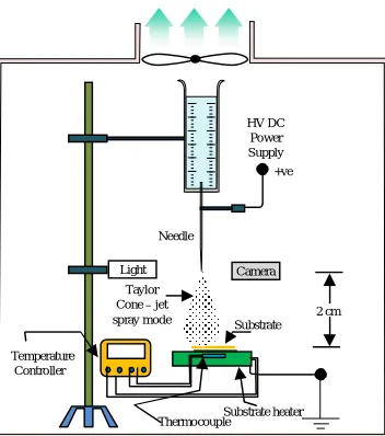
were deposited on glass substrates employing locally – made electrostatic spray deposition whose main components set up is illustrated in the schematic diagram of Figure 1. It is essentially made up of a precursor solution, electrostatic HV DC power supply, precursor atomization nozzle assembly, and a temperature – controlled hot plate heater.The atomizer has an adjustable steel capillary tube of 0.25 mm inner diameter nozzle clamped to a holder and supported by a metal tripod. The prepared precursor solution to be sprayed is flowing through the nozzle due to gravity with a flow rate ranging from 0.2 to 1 mL/min. For the DC high voltage power supply used in measurements, a simple high frequency (14 – 42 kHz) and variable duty cycle circuit is built. The NE 555 timer drives the flyback transformer in the “Flyback mode”. What that means is that the IRFP450 mosfet for the circuit is turned on by the timer, and current starts to flow through the manually – wound, 7 – turn primary windings. After some time the timer will turn off the mosfet again and the current will be forced to stop. However, this is not possible since the primary has significant inductance. The current then causes the voltage at the mosfet drain to increase in an attempt at allowing current to flow. The voltage will rise up to the breakdown voltage of the mosfet, where it stops (since the mosfet is avalanche rated this does no harm, and only produces heat in the mosfet). The voltage at the mosfet drain will potentially be equal to the breakdown voltage of the mosfet, meaning the primary voltage will be hundreds of volts now. Due to the large turns ratio of the flyback the few hundred volts at the primary become several thousand volts on the secondary. Since some energy is avalanched in the mosfet, adequate heat sinking of the IRFP450 is required. If it is desirable to power it from an even higher voltage, a snubber or stronger mosfet is used instead. The additional circuitry simply isolates the 555 from the "power" supply, so it can be increased beyond the 16V rating of the NE555. One thing to keep in mind is that the standard 7812 regulators should only run from 30 volts maximum, so for 50 volts input one needs to cut out the 7812 and run the logic section
from a dedicated supply.
Due to the high voltage applied at the metal needle, a Taylor cone - jet is created at the tip of the nozzle and the solution disrupts upon the droplets charge density reach Rayleigh limit after which the spray starts [7].
2.2 Precursor solution
A 0.2 M concentration aqueous precursor solution of stannous chloride dihydrate SnCl2.2H2O (molecular weight 225.63
g/mole) has been prepared by dissolving a solute quantity of 4.5126 g of SnCl2.2H2O in 100 mL isopropyl alcohol C3H9O
(the solvent). A magnetic stirrer is incorporated for this purpose for about 10 – 15 minutes together with addition of 0.1 mL hydrochloric acid to facilitate the complete dissolution of the solute in the solvent.
Prior to depositing the films, the commercial glass substrates were thoroughly cleaned in distilled water and dried in air for five minutes. After that, they were soaked in alcohol to remove any stains and contaminants. The electrostatic spray is conducted at substrate temperature within 450 ± 5 °C during the deposition. Film thickness is controlled by both the precursor concentration and the number of sprays, or alternatively, spraying time. Thus, a 4 – second spray time is maintained during the experiment. The normalized distance between the spray nozzle and substrate was fixed at 2.5 cm.. The spray rate of solution was maintained at 0.2 mL min.-1 throughout the experiment.
The possible chemical reaction that takes place on the heated substrate to produce SnO2 thin film may be described by the
following reaction [12]:
The precipitated SnO2 on the glass substrate was in the form of nanocrystals which is clearly identified by the AFM
morphology study of the SnO2 nanofilms.
Figure 1 Electrostatic Spray Deposition (ESD) experimental set up
Substrate
Substrate heater Thermocouple Temperature
Controller
Taylor Cone – jet spray mode
Needle
HV DC Power Supply
2 cm Ventilation Fan
+ve
Volume 3, Issue 3, March 2014
Page 396
2.3 Surface sensitization by palladiumMetal oxide gas sensors need a catalyst deposited on the surface of the film to accelerate the reaction and to increase the sensitivity, impart speed of response and selectivity [16].
Small amounts of noble metal additives, such as Pd or Pt are commonly dispersed on the semiconductor as activators or sensitizers to improve the gas selectivity, sensitivity and to lower the operating temperature [16],[17]. Many methods have already been tested for this purpose, for example bulk doping during calcination, sol-gel technology, spray pyrolysis deposition, thermal evaporation, CVD, laser ablation, magnetron sputtering, electroless addition. With the help of these methods, it was possible to form on a surface of metal oxides surface clusters of various components with sizes from 0.1 to 8 nm [1].
For the above reasons, the surface of the deposited SnO2 thin films were catalyzed using successive multiple spraying of
the prepared samples with a 50 ccm (0.0564 Molar) solution made up of dissolving 1% by weight palladium chloride PdCl2 (Mwt.= 177.3256 g/mole) in ethanol alcohol C2H5OH. Each sample was successively sprayed 20 times of 4s spray
interval and at 400 degrees hot plate heater temperature. Eventually, the sensitized samples were heat – treated at the same temperature for a period of one hour in atmospheric air.
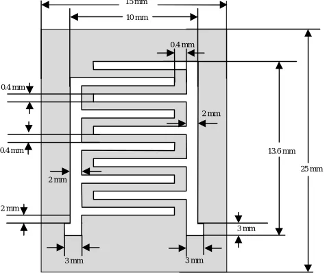
A 10 – finger aluminum mask of 0.4 – mm finger spacing is used to thermally evaporate the aluminum interdigitated electrodes IDE layer on the SnO2 sample. Figure 2 shows a schematic diagram of the mask utilized in this work.
2.4 Gas sensor testing system
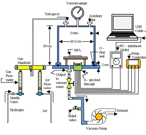
The fabricated gas sensor testing unit is illustrated in Figure 3. The unit consists of a vacuum – tight stainless steel cylindrical test chamber of diameter 163 mm and of height 200 mm with the bottom base made removable and of O – ring sealed. The effective volume of the chamber is 4173.49 cc; it has an inlet for allowing the test gas to flow in and an air admittance valve to allow atmospheric air after evacuation. Another third port is provided for vacuum gauge connection.
A multi-pin feed through at the base of the chamber allows for the electrical connections to be established to the sensor and the heater assembly. The heater assembly consists of a hot plate and a k – type thermocouple inside the chamber in order to control and set the desired operating temperature for the sensor. The thermocouple senses the temperature at the surface of the film exposed to the analyte gas. The PC – interfaced multi meter, of type UNI-T UT81B, was used to register the variation of the sensor conductance (reciprocal of resistance) exposed to predetermined air – hydrogen gas mixing ratio.
The chamber can be evacuated using a rotary pump to a rough vacuum of . A gas mixing manifold was incorporated to control the mixing ratios of the test and carrier gases prior to being injected into the test chamber. The mixing gas manifold is fed by zero air and test gas through a flow meter and needle valve arrangement. This arrangement of mixing scheme was done to ensure that the gas mixture entering the test chamber is premixed thereby giving the real sensitivity.
X-ray diffraction (XRD) was performed with a SHIMADZU 6000 diffractometer using Cu K radiation (1.5406 Å) in reflection geometry. A proportional counter with an operating voltage of 40 kV and a current of 30 mA was used. XRD patterns were recorded at a scanning rate of 0.08333° s-1 in the ranges from 20° to 60°.
Figure 2 A schematic diagram of the IDE mask utilized in this work
0.4 mm
0.4 mm
3 mm
3 mm
0.4 mm
13.6 mm
2 mm
3 mm 10 mm
15 mm
25 mm 2 mm
Volume 3, Issue 3, March 2014
Page 397
Figure 3 Gas sensor testing system20 cm
16.3 cm
8 – pin feed through Output
to vacuum pump Test gas in
Gas Manifold 2 cm O – ring seal
V A
Needle Valve Vacuum gauge 3 mm Auxiliary inlet 4 4 Gas Flow meter SnO2 Sensor
PC – interfaced DMM Temp. Controller Exhaust USB Cable Air Flow meter
Hydrogen Air
Relief valve
Vacuum Pump
The optical properties of SnO2 films were carried out with a UV-Vis spectrophotometer (model Optima sp-3000 plus) in
the UV/VIS/NIR regions. The optical transmittance at normal incidence was recorded in the wavelength range of 300-850 nm.
Surface morphology of the SnO2 sensing film was imaged by atomic force microscope model AA3000 Scanning Probe
Microscope SPM from Angstrom Advanced Inc.
3.
R
ESULTS ANDD
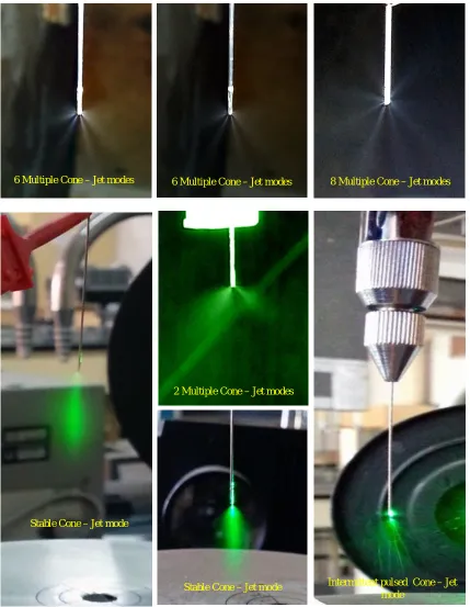
ISCUSSIONS 3.1 Electrostatic Spray Deposition ModesThe sensing tin oxide elements were prepared via the electrostatic spraying technique in which the applied high voltage DC at the syringe needle was varied between 3 – 20 kv and grounding the substrate. Different spray modes were observed during experiments. The most commonly encountered modes are shown in figure 4 and are referred to as: dripping mode, spindle mode, pulsed cone – jet mode, cone – jet mode, and multi – jet mode. The specific spray mode depends strongly on the geometry of the nozzle (capillary diameter), the strength and shape of the electric field and the liquid flow rate and its chemical composition. These spray modes are particularly sensitive to the physical properties of the liquid such as surface tension, viscosity, density, and electrical conductivity. The dripping mode generated the largest observable droplets which can be millimeter in diameter and even larger than the needle orifice diameter. On the other hand, the cone – jet and multi – jet modes produced the finest, mono – disperse, and high charge to mass ratio droplets with droplet diameters of submicron. The spindle mode and the pulsed cone – jet mode produced undesirable droplets since these having large distribution in size and charge.
3.2 Crystalline Structure and morphology
It is known that tin dioxide has a tetragonal rutile crystalline structure (known in its mineral form as cassiterite) with point group D_4h^14 and space group P42/mnm [13]. The unit cell consists of two metal atoms and four oxygen atoms. Each metal atom is situated amidst six oxygen atoms which approximately form the corners of a regular octahedron. Oxygen atoms are surrounded by three tin atoms which approximate the corners of an equilateral triangle. The lattice parameters are a= 4.7382 Å, and c= 3.1871 Å. Figure 5 shows the X-ray diffraction (XRD) pattern of the SnO2 thin film
prepared on glass substrate at 450 °C spray temperature. The major diffraction peaks of some lattice planes can be indexed to the tetragonal unit cell structure of SnO2 with lattice constants a= 4.738 Å and c= 3.187 Å, which are consistent with the standard values for bulk SnO2 (International Center for Diffraction Data (ICDD), PDF File No.
77-0447). The (hkl) peaks observed are (110), (101), (200), (211), (220), and (002). No characteristic peaks belonging to other tin oxide crystals or impurities were detected. In our films, the XRD spectrum showed predomination of the peaks, corresponding to reflection from the crystallographic (110), (101) planes, parallel to the substrate. The intensity of other peaks is small. It indicates that our films are textured.
At that, the degree of the texturing depends on kind of sprayed solution we used, and increases while using water solution instead of alcohol solution of SnCl2.
Volume 3, Issue 3, March 2014
Page 398
3.3 Optical characteristicsThe as-deposited SnO2 thin films were found to be highly transparent in the visible wavelength region with an average
transmittance of 80%. The optical energy gap Egap was derived assuming a direct transition between the edges of the
valence and the conduction bands, for which the variation in the absorption coefficient with the photon energy hν is given by:
6 Multiple Cone – Jet modes 8 Multiple Cone – Jet modes
2 Multiple Cone – Jet modes
Stable Cone – Jet mode 6 Multiple Cone – Jet modes
Figure 4 Electrostatic spraying modes
Intermittent pulsed Cone – Jet mode
Volume 3, Issue 3, March 2014
Page 399
Where in Eq. (2), is the absorption coefficient, Egap denotes the optical energy gap between the valence and theconduction bands. “Tauc” plots of α2 versus give the optical band gap value Egap by extrapolation of the linear region
of the resulting curve.
The calculated values of the direct optical energy gap varied between 3.49 and 3.79 eV for SnO2 thin films depending on
film thickness. The variations of the optical energy gap could be attributed to changes in the film defect density.
The band gap decreases with the increase of the film thickness from 145 nm to 466 nm. The decrease of band gap with the increase of film thickness implies that SnO2 is an n-type semiconductor [14]. This decrease of band gap may be
attributed to the presence of unstructured defects, which increase the density of localized states in the band gap and consequently decrease the energy gap [15].
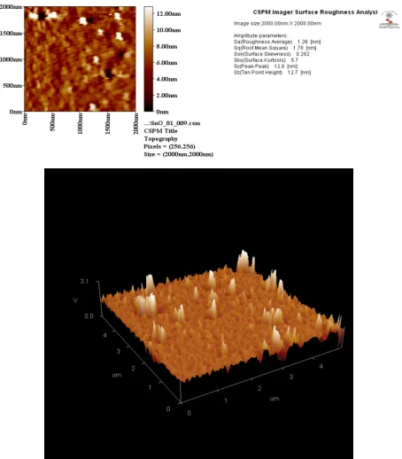
The surface morphology of the undoped SnO2 thin films as revealed by the AFM image is shown in Figure 6 on a
scanning area of 2000 nm x 2000 nm. The average roughness, Ra of sample is in the order of 1.26 nm, whereas the peak-to-valley roughness, RPV takes value of up to 12.8 nm. This result indicates that the coating surface morphology of SnO2
thin films is almost perfectly smooth with nanosize grains. The estimated grain size of undoped films is in the range of 57.6 – 68.8 nm.
Figure 5 X-ray diffraction (XRD) pattern of SnO2 thin film electrostatically – spray
deposited on glass substrate at temperature of 450 oC
Figure 6 AFM image of undoped SnO2 thin film deposited at 450 o
Volume 3, Issue 3, March 2014
Page 400
3.4 Sensing PropertiesThe gas response of the resistive sensor S is defined by the ratio of the film resistance in test gas to its resistance in air. The response of the sensor is affected by the geometrical factor K, the electronic characteristics term of the sensing element and the adsorption induced band bending term as in the following relation, Lupan [16]:
where K=4/Dλ (Dλ is the Debye length of sensing material) and no is the carrier concentration in air. VSa and VSg are the
absorbance-induced band bending potential in air and in H2 gas, respectively. Enhancement of the sensor sensitivity to H2
gas can be accomplished by controlling the above three terms via doping, modulating the operating temperature, or by altering the geometric parameters. In our work, sample doping with palladium highly increased the adsorption of hydrogen gas on the electrostatically – sprayed SnO2 surface, and thus modulating the surface depletion region thickness
through the variation of the charge carrier concentration.
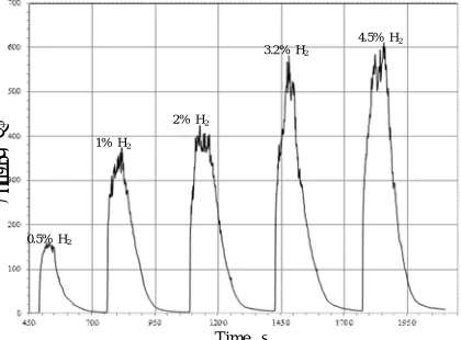
Figure 7 shows the switching behavior of the SnO2 gas sensor followed film surface modification with 15 palladium
chloride PdCl2 layers. A drastic enhancement in sensor sensitivity towards hydrogen gas is achieved in which, the sensor
maximum current increased upon being exposed to various hydrogen gas concentrations. The temperature at which the test was carried out was 200 0C with a 10 – v bias voltage. A relatively short response time of about 24 s was noticed at 2% hydrogen gas concentration.
3.5 Optimum operation temperature of the sensor
One of the most important disadvantages of SnO2 gas sensors is the high temperature required for the sensor operation
(200-500 0C) [17]. For that reason, the effect of the operation temperature on the thin films sensitivity was studied with the aim of optimizing the operation temperature to the lowest possible value [18], [19].
Figure 8 Variation of sensor response current of Pd - doped SnO2 thin film
exposed to4.5% hydrogen gas mixing ratio in air and at 10 bias voltage. Figure 7 Response transient of Pd – doped SnO2 gas sensor to different H2 : air
mixing ratios. The test performed at 200 degrees temperature and 10 v bias Time s
C
u
rr
en
t
μ
A
0.5% H2
1% H2
2% H2
3.2% H2
Volume 3, Issue 3, March 2014
Page 401
The gas sensitivity tests performed at room temperature show no variation on the film conductivity, even with the increase of the gas concentration. The increase in the operation temperature leads to an enhancement of the films sensitivity as it has been expected [20]. In Figure 8 we depict the dependence of maximum current on the temperature used. The best operating temperature for hydrogen sensor based on Pd – doped SnO2 thin film is around 2100
C. It can be noticed from the figure that the SnO2 film shows a volcano – shaped sensing trend where it shows negative temperature
coefficient of resistance up to 200 0C, whereas above 210 0C, a positive temperature coefficient of resistance is dominated.
4. Conclusions
In summary, SnO2 thin film sensors for hydrogen were prepared by a simple and cost – effective set up of electrostatic
spray technique. This technique provides easy control of the surface morphology and has proved to be efficient deposition method compared to other techniques, which are more or less sophisticated and expensive. The XRD results proved the high intensity of (110) and (101) peaks implying that these thin films mainly consist of the crystalline phase, while the AFM showed the nanostructure shape of the produced SnO2 films. Gas sensing properties of the device has been
investigated by which the optimum operating temperature was found to be around 210 0C. Sensors doped with palladium greatly affected the sensitivity to hydrogen gas and the latter increased with increasing hydrogen concentration levels. Fast response time of 24 s was obtained.
References
[1] Naoyoshi Taguchi, US patent 3,644,795, 1972. [2] FIGARO products catalog, pag. 2, 1990.
[3] Ying Liu, Erik Koep, and Meilin Liu, “A highly sensitive and fast-responding SnO2 sensor fabricated by combustion
chemical vapor deposition,” Chem. Mater., 17, pp. 3997-4000, 2005.
[4] GOURAI H., LUMBRERAS M., VAN LANDSCHOOT R. C. et al., “Elaboration and characterization of SnO2
-Mn2O3 thin layers prepared by electrostatic spray deposition”, Sensors and Actuators B: Chemical, vol. 47, p.
189-190,1998.
[5] Camelia MATEI GHIMBEU, “Preparation and Characterization of metal oxide semiconductor thin films for the detection of atmospheric pollutant gases”, University Paul Verlaine of Metz, France, Ph. D. Thesis, 2007.
[6] JAWOREK A., KRUPA A., “Classifications of the modes of EHD spraying”, Journal of Aerosol Science, vol. 30, p. 873-893, 1999.
[7] Matthias S. Wilm, Matthias Mann, “Electrospray and Taylor – Cone theory, Dole’s beam of macromolecules at last?”, International Journal of Mass spectrometry and Ion Processes”, 136, pp. 167 – 180, 1994.
[8] Yamazoe N, “Effects of additives on semiconductor gas sensors,” Sensors and Actuators, Volume 4, pp. 283-289, 1983.
[9] E. Elangovan, K. Ramamurthi, “Optoelectronic properties of spray deposited SnO2:F thin films for window materials
in solar cells,” Journal of Optoelectronics and Advanced Materials Vol. 5, No. 1, pp. 45 – 54, March 2003.
[10]Chanipat Euvananont, Thamrong Chansawang, Yot Boontongkong, Chanchana Thanachayanont, “Microstructural and electrical investigation of SnO2 twinned crystalline thin films deposited by spray pyrolysis,” Journal of
Microscopy Society of Thailand 23(1), pp. 79-82, 2009.
[11]George.Kiriakidis, K.Moschovis, I. Kortidis, “Gas sensors based on metal oxide spreypyrolysis films,” Proceeding of ICNM 1st International Conference on Nanostructured Materials and Nanocomposites, Kottayam, India, 6 – 8 April, 2009.
[12]E. Arca, K. Fleischer,* and I. V. Shvets, “Influence of the precursors and chemical composition of the solution on the properties of ZnO thin films grown by spray pyrolysis,” J. Phys. Chem. C 113, pp. 21074–21081, 2009.
[13]Sergiu T. Shishiyanu, Teodor S. Shishiyanu, Oleg I. Lupan, “Sensing characteristics of tin-doped ZnO thin films as NO2 gas sensor,” Sensors and Actuators B 107, pp. 379–386, 2005.
[14]K S Shamala, L C S Murthy and K Narasimha Rao, “Studies on tin oxide films prepared by electron beam evaporation and spray pyrolysis methods, “Bull. Mater. Sci., Vol. 27, No. 3, pp. 295–301, June 2004.
[15]G. Korotcenkov, J. Schwank, M. DiBattista, V. Brinzari, “XRD study of gas sensitive SnO2 thin films deposited by
spray pyrolysis method,” Semiconductor Conference, 1999. CAS '99 Proceedings. 1999 International IEEE Xplore, pp. 319 – 322, 1999.
[16]O. Lupan, V.V. Ursaki, G. Chai, L. Chowa, G.A. Emelchenko, I.M. Tiginyanu, A.N. Gruzintsev, A.N. Redkin, “Selective hydrogen gas nanosensor using individual ZnO nanowire with fast response at room temperature,” Sensors and Actuators B 144, pp. 56–66, 2010.
[17]V. Brinzari, G. Korotcenkov, J. Schwanka, Y. Boris, “Chemisorptional approach to kinetic analysis of SnO2:Pd-
based thin film gas sensors,” Journal of Optoelectronics and Advanced Materials, Vol. 4, No. 1, pp. 147 – 150, March 2002.
Volume 3, Issue 3, March 2014
Page 402
[19]Ying Liu, Erik Koep, and Meilin Liu, “A highly sensitive and fast - responding SnO2 sensor fabricated bycombustion chemical vapor deposition,” Chem. Mater., 17, pp. 3997 – 4000, 2005.
[20]F. Paraguay D and M. Miki Yoshida, “Doping effects on the response of thin film ZnO gas sensor to ethanol vapour,” superficies y Vacio, 9, pp. 245 – 247, 1999.
AUTHOR
Mazin S. Al-Ansari, M.Sc. Senior engineer – Physics Department- College of Science – Baghdad University. He received his master degree in medical dental engineering from Ulm University-West Germany. Currently, he is involved with designing electronic networks for post graduate students. Engineer Al-ansari main interest is in designing of electronic medical circuits.
Qahtan G. Al-zaidi received a B. Sc. (1994), M. Sc. (1997), and his Ph. D. (2012) in Optoelectronics from Baghdad University, Baghdad, Iraq. He was a lecturer at the optics lab of the Physics Department – College of Science of Baghdad University during the period 1997 –2007. He is currently a researcher at the department of Physics, Nanotechnology and Optoelectronics Research Group. Dr. Al-zaidi main interests are the development of chemical sensors based on semiconductor metal oxide nanostructured materials.