Please cite this article as: H. Rahimpour, M. Gholami, G. Ardeshir, H, MiarNaimiLow Settling Time All DigitalDLL for VHF Application, International Journal of Engineering (IJE), TRANSACTIONS B: Aspects Vol. 28, No. 3, (March 2015) 419-425
International Journal of Engineering
J o u r n a l H o m e p a g e : w w w . i j e . i rLow Settling Time All Digital DLL for VHF Application
H. Rahimpoura, M. Gholami*b, G. Ardeshirc, H, MiarNaimic
aDepartment of Electrical Engineering, University of Tehran, Iran
bDepartment of Electrical and Electronic Engineering, University of Mazandaran, Iran
cDepartment of Electrical and Computer Engineering, BabolNoshirvani University of Technology, Iran
P A P E R I N F O
Paper history: Received 20 May 2013
Received in revised form 17May 2014 Accepted 18November 2014
Keywords:
DLL
Delay Locked Loop PRP Conjugate Gradient Algorithm Synthesizer
A B S T R A C T
Delay Locked Loops (DLLs) and Phase Locked Loops (PLLs) are commonly used as a synthesizer or clock and data recovery circuit in most of the communication systems. In this paper, a new DLL is designed based on PRP conjugate gradient algorithm. The proposed DLL do not need any phase frequency detector, charge pump and loop filters, hence it can contribute better jitter performance and higher speed in comparison with conventional DLLs. In this design, PRP conjugate gradient algorithm is used to optimize the delay amount of each delay cells therefore helps the DLL to lock more accurately and quickly compared with gradient algorithm. In addition, for applying the PRP conjugate gradient algorithm a digital signal processor is used in the proposed architecture. To show the accuracy of the proposed structure’s operation, simulation has been done for 15 delay cells and fREF is chosen 14MHz to
have output frequency 14×15=210MHz. fOUT=210 MHz is one of the channels in Iran VHF frequency
band. As shown with simulation, the proposed architecture has a locking time of approximately 286nsec which is equal to 4 clock cycles of the reference clock.
doi: 10.5829/idosi.ije.2015.28.03c.11
1. INTRODUCTION1
Nowadays, Delay Locked Loops (DLLs) and Phase Locked Loops (PLLs) are widely used in communication systems. They are applied in most of the clock synchronization circuits [1, 2], frequency synthesizers [3, 4], digital transceivers [5], RAMs [6, 7] and clock and data recovery circuits [8]. One of the most important parameter in design of transceivers is related to their jitter contribution. DLLs have better jitter performance than PLLs. Hence, in recent years they are widely used in communication systems [9, 10]. In addition, DLLs are used as a clock multiplier or synthesizer to multiply the reference frequency and control the carrier frequency of different channels [11]. Application of DLLs is increasing rather than PLLs because of the faster locking process [12], lower phase noise [13], lower jitter [14], and better stability conditions.
1*Corresponding Author’s Email:[email protected] (M.
Gholami)
There are some design challenges in DLLs which show their performance. Speed limitations, settling time, working frequency, power consumption and their performance are the most important challenges in the design of DLLs. The conventional DLLs suffer from large lock time (their lock time is in the range of 50 and more clock cycles). Hence, new works in the field of DLL try to implement DLLs with lower lock time. Examples of high speed DLLs are [15] and [16] which proposed fast lock and wide range DLL, however, they need 15 and 22 clock cycles to lock, respectively. In high frequency application, it is still required to decrease the number of clock cycles to lock. In this regard, [12] propose a new digital with better lock time rather than pervious works. In this design, gradient algorithm is used for DLL architecture to reach better lock time. Also, a high speed DLL based frequency synthesizer is designed in [11] to cover VHF frequency band by using gradient algorithm. As we can see, nowadays having high speed DLLs is of importance. Therefore, to improve lock time of DLLs, a new all-digital and fast lock DLL-based frequency multiplier is proposed in this paper. One of the main advantages of
the proposed circuits is that it uses a digital signal processor instead of the phase-frequency detector, charge pump and loop filter. This results in the smaller chip area and locking time than conventional DLLs. To find optimized values for each delay cell, the PRP Conjugate Gradient algorithm is applied to the structure which has more speed than gradient algorithm. PRP Conjugate Gradient algorithm controls the error signal, which is defined as the difference of input and output signal tend to zero. Therefore, when the error signal becomes zero, input and output signals are exactly in phase, which is also needed in DLLs.
The paper is organized as follows. The next section describes the PRP Conjugate Gradient Algorithm and the proposed all-digital fast lock architecture for DLL-based frequency multipliers DLL-based on the limitation of conventional DLLs. Simulation and results will be presented in Section 3. Section 4, concludes the paper.
2.PROPOSED FAST-LOCK DLL BASED ON PRP CONJUGATE GRADIENT ALGORITHM
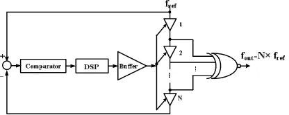
Conventional DLL-based frequency multiplier consists of a Voltage Controlled Delay Line (VCDL), a Phase-Frequency Detector (PFD), a Charge Pump (CP), a first- order Loop Filter (LF) and an Edge Combiner. In the locked condition, the output of the last delay stage is exactly one cycle lagged from the reference clock. Assuming similar delay cells are used in the signal path, the resulting delay of each of them is equal to TREF/N, where N is the number of delay cell and TREF is the period of a reference signal. When the DLL is locked, the edge combiner combines the edges of delay stages output’s to produce an integer multiple of the input frequency. In this case when N is even, the maximum output frequency is (N/2)×fREF and when N is odd, the maximum output frequency is N×fREF[17].
Conventional DLL based frequency multipliers occupy large area because of using capacitors in VCDL and LF [12]. Other parameters which are needed to be improved in conventional DLLs are locking time and working frequency.Also, there is another important limitation for conventional DLL-based frequency multipliers which is called a limited locking range. The DLL can be locked only when the following non-equality is satisfied [18]:
≤ ≤ (1)
where is the period of reference clock and the delay of the VCDL. If a delay of VCDL is in a range of (1) in whole time domain, the DLL can lock properly. Hence, harmonic lock and false lock cannot happen. Optimization problems naturally arise from applications such as signal processing, data analysis, network design, etc. Among many applications, error signal optimization
(minimization) has attracted much attention. The general form of the optimization problem is to minimize (or maximize) ( )where ∈ .
One of the simplest and most efficient methods to solve the above equation is a gradient method proposed by Cauchy in [19]. In this method, the value of x is calculated by the following recursive relation:
= − (2)
where =∇ ( ) is the gradient of ( ) at = . Obviously, this method is useful when the gradient of ( ) is available and is not complicated to obtain. is a coefficient that determines the convergence speed. In general form, x is n-dimensional. So, gradient vector is used in (3) to form n-dimensional variable in recursive relation, but in this paper target function for optimization has one-dimensional variable. Hence, gradient in general recursive relation (3) is replaced with derivative. As a result, (3) is converted to:
= − ( ) (3)
The larger the value of , the faster the convergence speed. It should be noted that if this coefficientisso large, then the system will be unstable. The gradient algorithm experiences a constant evolutionary path to reach the optimum solution. So, gradient algorithm has some drawbacks ([20, 21]) such as low convergence speed. in (2) can be considered as a variable value depending on the instantaneous gradient value. In this situation convergence of ( ) can be expedited.
One of the most powerful methods for solving optimization problems is conjugate gradient due to its simplicity and low memory requirements. This method has proper performance especially for large-scale optimization problems. The general form of this algorithm is:
= − (4)
where is a scalar, and is considered as:
=− ( ) + , =− ( ) (5)
is a scalar in the above equation. Relations (4) and (5) form the core of the conjugate gradient algorithm. Also, can be considered as a variable value which changes with the instantaneous gradient and x values. There are several relations for which identify different methods of the conjugate gradient algorithm[22-26]. One of the most efficient relations for in the point of computational view, is the following PRP (Polak Ribiere Polyak) method in which will be calculated as follows:
= ( )
‖ ‖ (6)
where and are representing the gradient values
conjugate gradient algorithm will be obtained as follows:
=− + ( )
‖ ‖ (7)
with changes convergence speed will not be linear. Thus, the performance of the conventional gradient method will be improved. In the next section, PRP conjugate gradient algorithm is used to find an optimum value for delay of each delay cells in proposed DLLs. As it has been shown in pervious section, conventional DLLs contain VCDL, CP, LF and PFD. It will be shown that these blocks can be substituted by a powerful digital signal processor (DSP). Therefore, input and output signals should be compared in a way to keep the phase difference exactly equal to TREF between them. To determine feedback path of the proposed DLL an error signal is needed which should be optimized by a PRP conjugate gradient algorithm which will be explained in this section.
The general form of square signal is written as:
( ) = sin + sin 2 + sin 3 +⋯ (8)
Due to intrinsic delay in each signal path, the output signal can be written as ( − ). In other words, output signal is defined as input signal with delay of ,where is the intrinsic delay in sthe signal path and it is a very small value. Due to intrinsic delay of VCDL, cannot be zero and in DLLs, a delay is needed to synchronize input and output of the VCDL. Hence, some blocks should be added to make the delay of signal path equal to TREF. Having similar delay blocks in the signal path with the same delay of , the total amount of delay will be . As a result, a feedback path should be added to control the amount of to set it to in the lock condition. By using N delay cells, the
output signal can be written as:
( ) = ( − ) (9)
The added feedback path should be controlled adaptively. Hence, a signal is required to identify the phase difference between the input and output signals. This signal can be obtained by subtracting the input signal from the output signal. So:
( ) = ( )− ( ) = (sin ( − )−sin ) + (sin2 ( − )−sin 2 ) + (sin3 ( −
)−sin 3 ) +⋯ (10)
This signal is known as an error signal which should tend to zero. When this error signal is equal to zero, then the output signal will be exactly in phase with the input signal. In this situation each cell propose a delay value of .
The target function for optimization is equal to:
( ) = | ( )| (11)
The PRP conjugate gradient algorithm is used in the feedback path to control the amount of each delay cell dynamically. The reference signal which is used in this control process is ( ). This means that is changed with the reference signal ( ) by using an adaptive conjugate gradient algorithm. Since, ( ) is a real function, | ( )| is equal with ( ).
To obtain a recursive relation for , it is essential to calculate ( )
as:
()
= ()
= [ ( ( − )− ) + ( 2 ( − )− 2 ) + ( 3 ( −
)− 3 ) +⋯]
(12)
The above equation will be arranged to: ()
=−2 ()
[ ()− ()] =−2 ()
( ) (13) As a function f(x) in Equation (2), the target function for optimization is Jμ(t). Therefore, according to the PRP conjugate gradient algorithm, the recursive relation for is:
= − (14)
where is:
=− ( )+ , =− ()
(15) Substituting (13) in (15) and according to PRP conjugate gradient algorithm, can be obtained:
=−2 ( ) ( ) + ()
( )
()
( )
, =−2 () (0)
(16)
It should be mentioned that each delay cell is controlled with the same recursive relation. Using this method, the speed of convergence can be measured by analyzing the time evolution of the locking process. The step size parameters, and are chosen as a constant value to reduce the system transient time.
According to the above equations, the proposed DLL structure can be obtained which is shown in Figure 1. According to this figure, the proposed architecture consists of a comparator, buffer, substractor, DSP, delay cells and an XOR gate. The input signal of DSP is the difference between input and output signals. DSP compute an optimum value of delay for each delay cell to have a zero error signal. It should be noted that, DSP in Figure 1 will not lead to consume any excess power for proposed DLL, because the presence of DSP in digital communication is inevitable and adding one more output and input ports in DSP will not change power consumption significantly. As an example, in transceivers which contain DLLs, a DSP is used for choosing different kinds of modulations [27]. Control signal of delay cells is provided from this DSP. This means PFD, CP, and LF is eliminated in the proposed architecture in comparison with conventional DLLs. Hence, power consumption and area of proposed architecture will be decreased significantly.
3. SIMULATIONS AND RESULTS
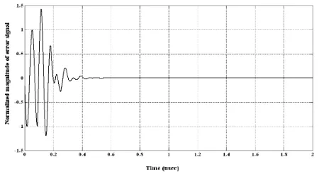
Simulation has been done for N=15 and = 14 to validate the function of the proposed all-digital fast lock DLL. Figure 2 shows the normalized magnitude of the error signal. When the output signal reaches about 95% of its steady state, it will be considered as lock condition. According to this figure, the error signal becomes zero after 286ns. This means that after 4 clock cycles, the proposed DLL will lock. In lock condition delay of each delay cells is equal with
=
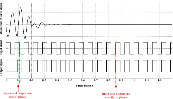
. = × × which is around 4.76 . Figure 3 shows the delay value of each delay cell. In lock condition where the output signal reaches about 95% of its steady state, the delay of each delay cell is equal to 4.76 . Figures2 and 3 show that the proposed structure can lock very fast in only 4 clock cycles. Low jitter functionality of our proposed DLLcan be proved by comparing the ripple of delay of each delay cell around its stable value and also the ripple of error signal (Figures 2 and 3). This work has little changes near the stable value, but other works propose more oscillation around their steady states which leads to more jitter of their works [17]. Figure 4 shows the related waveforms of the proposed all-digital fast lock DLL. This figure shows that output and input of the proposed architecture are exactly in phase after lock condition (output is one period lagged from input). This figure also illustrates that by combining edges of all delay stage's output with XOR gates, multiplied output frequency is = 15 × which is equal
to 210 .
Figure 4 shows the magnitude of error, input and output signals. This figure shows that around t=0.1µs, input and output signals of DLL are not in phase. In this case the magnitude of the error signal is not exactly zero. In other words, this signal shows that the input and output of the DLL have some phase differences.
Then, DSP forces the error signal to tend to zero by using a PRP conjugate gradient algorithm. As shown in Figure 4, after 4 clock cycles, the DLL is approximately locked. This figure also shows that after t=0.5µs, input and output of DLL are exactly in phase and the lock condition is completely obtained.Since the DSP block can be implemented by analog circuits, the proposed DLL will operate at higher frequencies and consume lower power and area than conventional DLLs. Similar works such as [15, 16, 28] and [29] need minimum of 15, 22, 32 and 34 clock cycles to be locked, respectively, while as the simulations show, the proposed architecture needs only 4 clock cycles. To have the correct lock in DLLs, Equation (1) should be satisfied.Itis the only limitation whichdoes not allow DLLs to work in higher or lower frequencies because of delay amount of more than 3T/2, DLL will have harmonic lock which causes an output signal to lag as much as mTREF (m is an integer greater than one) from the input signal.
Figure 2. Normalized Magnitude of Error signal
Figure 4 Transient waveforms of proposed all digital DLL to reach lock condition
Also, for a delay amount lower than T/2 DLL will not lock properly. The above explanations are the only limitations of DLLs lock range either in the circuit or system level design.It should be mentioned that in digital communication a processor should be used for example to choose different methods of modulations (Q-PSK, QAM,…) [27]. Hence, the delay is controlled by one of the outputs of this processor. In other words, no additional circuit is needed to control the delay of VCDL in the proposed structure. This means that the PFD and CP are eliminated in new architecture in comparison with conventional DLLs. Therefore, power consumption and area of proposed architecture will be lower than conventional DLLs.
4. CONCLUSIONS
A novel fast lock and high speed DLL-based frequency multiplier which has smaller area than conventional DLL is proposed in this paper. PRP conjugate gradient algorithm is used to control the delay of each delay cells in the VCDL. The output frequency is chosenas 210MHz to adopt with one of the Iran VHF band channels. To reach this goal, simulation has been done for 15 delay cells and fREF=14MHz. Simulations show that output frequency is multiplied by 14 (fOUT=210MHz), locking time is approximately 286nsec which is equal to 4 clock cycles of reference clock.
5. REFERENCES
1. Mandal, A. and Mishra, R., "Design and implementation of digital demodulator for frequency modulated CW radar (research note)", International Journal of Engineering-Transactions A: Basics, Vol. 27, No. 10, (2014), 1581-1590.
2. Gholami, M., Rahimpour, H., Ardeshir, G. and Miar‐Naimi, H., "A new fast‐lock, low‐jitter, and all‐digital frequency synthesizer for dvb‐t receivers", International Journal of Circuit Theory and Applications, (2013).
3. Gholami, M., Ardeshir, G. and Ghonoodi, H., "A novel architecture for low voltage-low power dll-based frequency multipliers", IEICE Electronics Express, Vol. 8, No. 11, (2011), 859-865.
4. Moallem, P. and Ehsanpour, M., "A novel design of reversible multiplier circuit", International Journal of Engineering, Vol. 26, No. 6, (2013), 577-586.
5. Coban, A.L., Koroglu, M.H. and Ahmed, K.A., "A 2.5-3.125-gb/s quad transceiver with second-order analog dll-based cdrs",
Solid-State Circuits, IEEE Journal of, Vol. 40, No. 9, (2005), 1940-1947.
6. Yun, W.-J., Lee, H.-W., Shin, D. and Kim, S., "A 3.57 gb/s/pin low jitter all-digital dll with dual dcc circuit for GDDR3 dram in 54-nm cmos technology", Very Large Scale Integration (VLSI) Systems, IEEE Transactions on, Vol. 19, No. 9, (2011), 1718-1722.
7. Kim, N.-S., Cho, U.-R. and Byun, H.-G., "Low voltage wide range dll-based quad-phase core clock generator for high speed network sram application", in Custom Integrated Circuits Conference, 2005. Proceedings of the IEEE 2005, IEEE, (2005), 533-536.
8. Gao, X., Klumperink, E.A. and Nauta, B., "Advantages of shift registers over dlls for flexible low jitter multiphase clock generation", Circuits and Systems II: Express Briefs, IEEE Transactions on, Vol. 55, No. 3, (2008), 244-248.
9. Oh, K.-I., Kim, L.-S., Park, K.-I., Jun, Y.-H. and Kim, K., "Low-jitter multi-phase digital dll with closest edge selection scheme for ddr memory interface", Electronics Letters, Vol. 44, No. 19, (2008), 1121-1123.
10. Gholami, M. and G. Ardeshir, "Dual phase detector based delay locked loop for high speed applications", International Journal of Engineering-Transactions A: Basics, Vol. 27, No. 4, (2014), 517-522.
11. Gholami, M., Rahimpour, H., Ardeshir, G. and MiarNaimi, H., "Digital delay locked loop-based frequency synthesiser for digital video broadcasting-terrestrial receivers", IET Circuits, Devices & Systems, Vol. 8, No. 1, (2014), 38-46.
Integrated Circuits and Signal Processing, Vol. 78, No. 3, (2014), 819-826.
13. Liao, F.-R. and Lu, S.-S., "A waveform-dependent phase-noise analysis for edge-combining DLL frequency multipliers",
Microwave Theory and Techniques, IEEE Transactions on, Vol. 60, No. 4, (2012), 1086-1096.
14. Gholami, M. and Ardeshir, G., "Jitter of delay-locked loops due to pfd", (2014).
15. Shin, D., Song, J., Chae, H. and Kim, C., "A 7 ps jitter 0.053 mm fast lock all-digital DLL with a wide range and high resolution dcc", Solid-State Circuits, IEEE Journal of, Vol. 44, No. 9, (2009), 2437-2451.
16. Cheng, K.-H. and Lo, Y.-L., "A fast-lock wide-range delay-locked loop using frequency-range selector for multiphase clock generator", Circuits and Systems II: Express Briefs, IEEE Transactions on, Vol. 54, No. 7, (2007), 561-565.
17. Gholami, M., "A novel low power architecture for DLL-based frequency synthesizers", Circuits, Systems, and Signal Processing, Vol. 32, No. 2, (2013), 781-801.
18. Y. Moon, D.-K. Jeong, G. Ahn and . "A 0.6-2.5-gbaud cmos tracked oversampling 3x transceiver with dead-zone phase detection for robust clock/data recovery", IEEE Journal of Solid-State Circuits, Vol. 36, No. 1974-1983.
19. Cauchy, A., "Méthode générale pour la resolution des systemes d’equations simultanées", Comp. Rend. Sci. Paris, Vol. 25, No. 1847, (1847), 536-538.
20. Akaike, H., "On a successive transformation of probability distribution and its application to the analysis of the optimum gradient method", Annals of the Institute of Statistical Mathematics, Vol. 11, No. 1, (1959), 1-16.
21. Forsythe, G.E., "On the asymptotic directions of thes-dimensional optimum gradient method", Numerische Mathematik, Vol. 11, No. 1, (1968), 57-76.
22. Dai, Y.-H. and Yuan, Y., "A nonlinear conjugate gradient method with a strong global convergence property", SIAM Journal on Optimization, Vol. 10, No. 1, (1999), 177-182. 23. Li, G., Tang, C. and Wei, Z., "New conjugacy condition and
related new conjugate gradient methods for unconstrained optimization", Journal of Computational and Applied Mathematics, Vol. 202, No. 2, (2007), 523-539.
24. Wei, Z.X., Li, G.Y. and Qi, L.Q., "Global convergence of the polak-ribiere-polyak conjugate gradient method with an armijo-type inexact line search for nonconvex unconstrained optimization problems", Mathematics of Computation, Vol. 77, No. 264, (2008), 2173-2193.
25. Yuan, G., "Modified nonlinear conjugate gradient methods with sufficient descent property for large-scale optimization problems", Optimization Letters, Vol. 3, No. 1, (2009), 11-21. 26. Yu, G., Zhao, Y. and Wei, Z., "A descent nonlinear conjugate
gradient method for large-scale unconstrained optimization",
Applied Mathematics and Computation, Vol. 187, No. 2, (2007), 636-643.
27. Kavalov, D. and Kalinin, V., "Neural network surface acoustic wave rf signal processor for digital modulation recognition",
Ultrasonics, Ferroelectrics, and Frequency Control, IEEE Transactions on, Vol. 49, No. 9, (2002), 1280-1290.
28. Chang, H.-H. and Liu, S.-I., "A wide-range and fast-locking all-digital cycle-controlled delay-locked loop", Solid-State Circuits, IEEE Journal of, Vol. 40, No. 3, (2005), 661-670.
29. Yang, R.-J. and Liu, S.-I., "A 40–550 MHZ harmonic-free all-digital delay-locked loop using a variable sar algorithm", Solid-State Circuits, IEEE Journal of, Vol. 42, No. 2, (2007), 361-373.
APPENDIX
To examine validation of Equation (14), the first two harmonics of the input signal are calculated. Differentiating of (11) with respect to , we have:
()
= [ (sin ( − )−sin ) + (sin2 ( − )−sin2 )] (A-1) This results in:
(A-2)
()
= [ (sin ( − ) + sin −2 sin ( − )sin ) + (sin 2 ( − ) + sin 2 − 2 sin 2 ( − ) sin 2 )] + 2 (sin ( − ) sin 2 ( − ) + sin sin2 −sin ( − ) sin 2 −
sin sin 2 ( − ))]
After applying a derivative operation to (A-2), we have:
()
= (−2 [sin ( − )cos ( − )−cos ( − ) sin ]−2 [2sin 2 ( − ) cos 2 ( − )−2 cos 2 ( − ) sin2 ]−2 [2sin ( − ) cos 2 ( − ) + cos ( − ) sin2 ( − )−
cos ( − ) sin2 −2 sin cos2 ( − )])
(A-3)
Rearranging this equation as:
(A-4)
()
= −2 ( cos ( − ) + 2 cos 2 ( − )) × ( sin ( − )− sin + sin 2 ( − )−
sin 2 )
( cos ( − ) + 2 cos2 ( − )) = () (A-5)
And:
sin ( − )− sin + sin 2 ( − )− sin 2 = ( )− () (A-6)
Substituting Equation (A-6) and (A-5) into (A-4), we obtain: ()
= −2 ()
[ ()− ()] (A-7)
The above equation is the same as (14). Therefore, Equation (14) has been proved for first two harmonics of Equation (7). Also, the same procedure can be applied to higher harmonics of the input signal to validate (14) for all harmonics.
Low Settling Time All Digital DLL for VHF Application
H. Rahimpoura, M. Gholamib, G. Ardeshirc, H, MiarNaimic
aDepartment of Electrical Engineering, University of Tehran
bDepartment of Electrical and Electronic Engineering, University of Mazandaran
cDepartment of Electrical and Computer Engineering, BabolNoshirvani University of Technology
P A P E R I N F O
Paper history: Received 20May 2013
Received in revised form 17May 2014 Accepted 18November 2014
Keywords:
DLL, Delay Locked Loop PRP Conjugate Gradient Algorithm
Synthesizer
هﺪﯿﮑﭼ
ﻪﻘﻠﺣ
ﺮﯿﺧﺎﺗهﺪﺷﻞﻔﻗيﺎﻫ
)
DLL
(
ﻪﻘﻠﺣو
زﺎﻓهﺪﺷﻞﻔﻗيﺎﻫ
)
PLL
(
هدﺮﺘﺴﮔرﻮﻃﻪﺑ هﺪﻨﻨﮐﺰﺘﻨﺳناﻮﻨﻋﻪﺑيا
وﯽﺴﻧﺎﮐﺮﻓيﺎﻫ
ﻢﺘﺴﯿﺳردهدادوكﻼﮐﯽﺑﺎﯾزﺎﺑيﺎﻫراﺪﻣ
ﯽﻣراﺮﻗهدﺎﻔﺘﺳادرﻮﻣﯽﺗاﺮﺑﺎﺨﻣيﺎﻫ ﺪﻧﺮﯿﮔ
.
ﮏﯾ،ﻪﻟﺎﻘﻣﻦﯾارد
DLL
ﺮﺑﯽﻨﺘﺒﻣﺪﯾﺪﺟ
جودﺰﻣنﺎﯾداﺮﮕﻤﺘﯾرﻮﮕﻟا
PRP
ﺖﺳاهﺪﺷﯽﺣاﺮﻃ
.
زﺎﻓزﺎﺳرﺎﮑﺷآﻪﺑ،هﺪﺷﻪﺋارارﺎﺘﺧﺎﺳ
-زﺎﯿﻧﻪﻘﻠﺣﺮﺘﻠﯿﻓورﺎﺑﭗﻤﭘ،ﺲﻧﺎﮐﺮﻓ
ﯽﻣﻦﯾاﺮﺑﺎﻨﺑ،دراﺪﻧ ﻪﻘﻠﺣلواﺪﺘﻣرﺎﺘﺧﺎﺳﻪﺑﺖﺒﺴﻧﺖﻋﺮﺳوﺮﺘﯿﺟظﺎﺤﻟزايﺮﺘﻬﺑدﺮﮑﻠﻤﻋﺪﻧاﻮﺗ
ﺪﺷﺎﺑﻪﺘﺷادﺮﯿﺧﺎﺗهﺪﺷﻞﻔﻗيﺎﻫ
.
رﺎﺘﺧﺎﺳﻦﯾارد ،
نﺎﯾداﺮﮕﻤﺘﯾرﻮﮕﻟا جودﺰﻣ
PRP
ﻦﯾاﻪﮐﺖﺳاﻪﺘﻓﺮﮔراﺮﻗهدﺎﻔﺘﺳادرﻮﻣﺮﯿﺧﺎﺗلﻮﻠﺳﺮﻫﺮﯿﺧﺎﺗندﺮﮐﻪﻨﯿﻬﺑﺖﻬﺟ
ﻖﯿﻗد ﻞﻔﻗ ﻪﺑ عﻮﺿﻮﻣ
ﻊﯾﺮﺳ و ﺮﺗ
ﻪﻨﯿﻬﺒﻤﺘﯾرﻮﮕﻟا ﻪﺑﺖﺒﺴﻧ ﺮﺗ
ﯽﻣ ﯽﻬﺘﻨﻣ نﺎﯾداﺮﮕﯾزﺎﺳ
دﻮﺷ
.
زا هدﺎﻔﺘﺳا ﺖﻬﺟ ،ﻦﯾا ﺮﺑ هوﻼﻋ
جودﺰﻣنﺎﯾداﺮﮕﻤﺘﯾرﻮﮕﻟا
PRP
ﺖﺳازﺎﯿﻧلﺎﺘﯿﺠﯾدشزادﺮﭘﺶﺨﺑﮏﯾﻪﺑ
.
ﻧياﺮﺑ ﻪﯿﺒﺷ،رﺎﺘﺧﺎﺳﻦﯾاﺖﻗدندادنﺎﺸ
ياﺮﺑيزﺎﺳ
15
يدوروﺲﻧﺎﮐﺮﻓبﺎﺨﺘﻧاﺎﺑﺮﯿﺧﺎﺗلﻮﻠﺳ
14
ﯽﺟوﺮﺧﺲﻧﺎﮐﺮﻓﺖﻓﺎﯾردﺖﻬﺟﺰﺗﺮﻫﺎﮕﻣ
210
ﺖﺳاﻪﺘﻓﺮﮔمﺎﺠﻧاﺰﺗﺮﻫﺎﮕﻣ
.
ﯽﺟوﺮﺧﺲﻧﺎﮐﺮﻓ
210
لﺎﻧﺎﮐزاﯽﮑﯾ،ﺰﺗﺮﻫﺎﮕﻣ
ﯽﺴﻧﺎﮐﺮﻓﺪﻧﺎﺑرددﻮﺟﻮﻣيﺎﻫ
VHF
ﺖﺳاناﺮﯾا
.
ﻪﯿﺒﺷردﻪﮐﻪﻧﻮﮕﻧﺎﻤﻫ يزﺎﺳ
ﺎﻫ
دادنﺎﺸﻧ دوﺪﺣردﯽﻠﻔﻗنﺎﻣزيدﺎﻬﻨﺸﯿﭘرﺎﺘﺧﺎﺳ،ﺖﺳاهﺪﺷه
286
ﺎﺑلدﺎﻌﻣﻦﯾاﻪﮐﻪﺘﺷادﻪﯿﻧﺎﺛﻮﻧﺎﻧ
4
ﺖﺳايدوروكﻼﮐﻞﮑﯿﺳ
.