Adv. Radio Sci., 9, 225–230, 2011 www.adv-radio-sci.net/9/225/2011/ doi:10.5194/ars-9-225-2011
© Author(s) 2011. CC Attribution 3.0 License.
Advances in
Radio Science
Reliability analysis of buffer stage in mixed signal application
S. More1, M. Fulde2, F. Chouard1, and D. Schmitt-Landsiedel1
1Lehrstuhl f¨ur Technische Elektronik,Technische Universit¨at M¨unchen, Germany 2Infineon Technologies AG, Villach, Austria
Abstract. This paper discusses reliability analysis of a buffer circuit targeted for an analog to digital converter application. The circuit designed in a 32 nm high-κ metal gate CMOS technology was investigated by circuit simulation and sensi-tivity analysis. This analysis was conducted for realistic time varying (AC) stress. As aging effects, negative and positive bias temperature instability, conducting and non-conducting hot carrier injection are taken into consideration. The ag-ing contributions of these effects on the different transistors in the buffer circuit and on different buffer performance fig-ures are evaluated. Using these results, the impact of an aged buffer circuit on the performance of a successive approxima-tion ADC circuit is evaluated. The most severely affected performance due to aging is amplifier offset, which leads to time varying gain error in the ADC circuit.
1 Introduction
Non-constant field scaling in nanoscale CMOS technology has led to undesirable reliability issues due to effects such as Negative Bias Temperature Instability (NBTI), Positive Bias Temperature Instability (PBTI), Conducting and Non-Conducting Hot-Carrier Injection (HCI,NCHCI). Significant device level research is carried out on these effects (Grasser et al., 2007; Kaczer et al., 2009). However, since the su-perposition of these effects in a circuit is quite complex, the study of their impact on circuit level is still in a preliminary stage (Jha et al., 2005; Martin-Martinez et al., 2009; Chouard et al., 2010a).
This paper targets to investigate the impact of aging on a buffer stage designed for Analog to Digital Converter (ADC) application. The circuit was implemented and simulated
us-Correspondence to: S. More
ing 32 nm high-κ metal gate regularVt hnMOS and pMOS devices (Chen et al., 2008), so the effect of PBTI which ap-pears due to high-κis also present. The effects of buffer cir-cuit degradation on ADC performance is demonstrated and the need for countermeasures is highlighted. The degradation effects are evaluated using a combination of sensitivity anal-ysis and circuit simulation. This methodology as described in (More et al., 2010) was developed, as it needs considerably less computing effort than sole use of circuit simulation, and it provides more intuitive insight into the various degradation contributions.
Section 2 presents the models used for aging simulation. The investigated buffer circuit topology is shown in Sect. 3. Section 4 discusses results of aging simulation of buffer cir-cuits. The analytical evaluation of these degradation effects using sensitivity analysis, its comparison with simulation re-sults and the observed impact on the circuit performance are presented in Sect. 5. Effects of buffer circuit aging on ADC performance and need of countermeasures are discussed in Sect. 6. A conclusion is given in Sect. 7.
2 Modeling of device degradation
Device degradation due to aging resulting from NBTI or PBTI mainly shifts the threshold voltage(Vt h)of MOS tran-sistors, whereas HCI and NCHCI reduce the transistor cur-rent(Id)and also give a smaller contribution to the threshold voltage shift. This can be modeled by replacing the MOS-FET with an equivalent circuit shown in Fig. 1. The Vt h
shifts are modeled by an equivalent voltage sourcevtshift in series to the gate terminal, the hot carrier effects by a current controlled current source (CCCS)I dshift between the drain and source terminal. The threshold voltage shift by each of the BTI effects can be modeled by(1Vt h)BTI as in Eq. (1). BTI stands for NBTI in pMOS transistors and for PBTI in nMOS transistors. The current degradation is modeled by
226 S. More et al.: Reliability analysis of buffer stage Manuscript prepared for Adv. Radio Sci.
with version 3.2 of the LATEX class copernicus.cls. Date: 23 December 2010
Reliability Analysis of Buffer Stage in Mixed Signal Application
S. More1, M. Fulde2, F. Chouard1, and D. Schmitt-Landsiedel1
1Lehrstuhl f¨ur Technische Elektronik,Technische Universit¨at M¨unchen, Germany
2Infineon Technologies AG, Villach, Austria
Abstract.This paper discusses reliability analysis of a buffer circuit targeted for an analog to digital converter application. The circuit designed in a 32nm high-κ metal gate CMOS technology was investigated by circuit simulation and sensi-tivity analysis. This analysis was conducted for realistic time varying (AC) stress. As aging effects, negative and positive bias temperature instability, conducting and non-conducting hot carrier injection are taken into consideration. The ag-ing contributions of these effects on the different transistors in the buffer circuit and on different buffer performance fig-ures are evaluated. Using these results, the impact of an aged buffer circuit on the performance of a successive approxima-tion ADC circuit is evaluated. The most severely affected performance due to aging is amplifier offset, which leads to time varying gain error in the ADC circuit.
1 Introduction
Non-constant field scaling in nanoscale CMOS technology has led to undesirable reliability issues due to effects such as Negative Bias Temperature Instability (NBTI), Positive Bias Temperature Instability (PBTI), Conducting and Non-Conducting Hot-Carrier Injection (HCI,NCHCI). Significant device level research is carried out on these effects (Grasser et al., 2007; Kaczer et al., 2009). However, since the su-perposition of these effects in a circuit is quite complex, the study of their impact on circuit level is still in a preliminary stage (Jha et al., 2005; Martin-Martinez et al., 2009; Chouard et al., 2010a).
This paper targets to investigate the impact of aging on a buffer stage designed for Analog to Digital Converter (ADC) application. The circuit was implemented and simulated us-ing 32nm high-κmetal gate regularVth nMOS and pMOS
Correspondence to:S. More ([email protected])
devices (X. Chen et al., 2008), so the effect of PBTI which appears due to high-κis also present. The effects of buffer circuit degradation on ADC performance is demonstrated and the need for countermeasures is highlighted. The degra-dation effects are evaluated using a combination of sensitiv-ity analysis and circuit simulation. This methodology as de-scribed in (More et al., 2010) was developed, as it needs con-siderably less computing effort than sole use of circuit simu-lation, and it provides more intuitive insight into the various degradation contributions.
Section 2 presents the models used for aging simulation. The investigated buffer circuit topology is shown in Section 3. Section 4 discusses results of aging simulation of buffer circuits. The analytical evaluation of these degradation ef-fects using sensitivity analysis, its comparison with simula-tion results and the observed impact on the circuit perfor-mance are presented in Section 5. Effects of buffer circuit aging on ADC performance and need of countermeasures are discussed in Section 6. A conclusion is given in Section 7.
2 Modeling of Device Degradation
Fig. 1.Models for MOSFETs with degradation
Device degradation due to aging resulting from NBTI or PBTI mainly shifts the threshold voltage(Vth)of MOS
tran-sistors, whereas HCI and NCHCI reduce the transistor cur-rent(Id)and also give a smaller contribution to the threshold
voltage shift. This can be modeled by replacing the
MOS-Fig. 1. Models for MOSFETs with degradation.2 S. More et al.: Reliability Analysis of Buffer Stage
Fig. 2.Schematic of buffer and DC level shifting circuit
FET with an equivalent circuit shown in Figure 1. TheVth
shifts are modeled by an equivalent voltage sourcevtshif tin
series to the gate terminal, the hot carrier effects by a current controlled current source (CCCS)Idshif tbetween the drain
and source terminal. The threshold voltage shift by each of the BTI effects can be modeled by(∆Vth)BT I as in
equa-tion (1). BTI stands for NBTI in pMOS transistors and for PBTI in nMOS transistors. The current degradation is mod-eled by equation (2), separately for HCI and NCHCI. The values of the equivalent sources are determined using (1)-(2), which describe the relation of different contributing factors to the overall degradation, similar to (Martin-Martinez et al., 2009; Huard et al., 2009). The totalvtshif tis the sum of two
contributions, see equation (3). The total current degrada-tion is modeled by equadegrada-tion (4). The model parameters were fitted to single device stress measurements.
(∆Vth)BT I=A·
Vgs
Tinv
m
·e(∆kTE)·Lα·Wβ·tn (1)
(∆Id)HCI/N CHCI=Id·B·Vdsp·e(
∆E kT)
·Lδ·tq (2)
vtshif t=a·(∆Vth)BT I+b·(∆
Id
Id )HCI
(3)
Idshif t=c·(
∆Id
Id
)HCI+d·(
∆Id
Id
)N CHCI (4)
For the evaluations based on circuit simulation and to ac-count for time varying (AC) stress, the aging simulation tool RelXpertT M (RelXpert, 2010) was used, which employs the above discussed models.
3 Buffer Circuit for ADC Application
The schematic for the fully differential buffer circuit is il-lustrated in Fig. 2a. It basically consists of an Operational Transconductance Amplifier (OTA), resistors and switches. Capacitors of 2pF are used to emulate the load of a Digi-tal to Analog Converter (DAC) connected at the output of the buffer circuit. The primary function of this buffer cir-cuit in the charge distribution based successive approxima-tion (SAR) ADC as depicted in Fig. 3 (Fulde et al., 2009), is to drive the DAC implemented using capacitors, within a short settling time (≈4ns) with reference voltage (Vref±)
Vin−
Vin+ Vout− Vout+ ain−
ain+ Vref−
Vref+
Buffer
SAR Logic
Digital Output
Fig. 3.Schematic of Successive Approximation ADC
and analog input(ain±)during different phases of the clock
signals that control the switches. The clock signals are shown only schematically, not displaying the more complex clock-ing durclock-ing the ADC operation.
The used OTA is illustrated in Fig. 4. It is a two stage folded cascode amplifier with Miller compensation. Imple-menting this circuit using regular Vth pMOS and nMOS
transistors with Vth≈0.45V and supply VDD=1V leads to
significant challenges in using the common mode voltage
Vcm=0.5V at the gate of input differential pair (N0andN1)
and maintaining the tail transistor (N3) in saturation. To
overcome this problem a simple level shifting circuit as de-picted in Fig. 2b was used at the input of the OTA. This cir-cuit shifts each input signal (Vin) of the OTA withVcm=0.5V
to a new shifted signal (Svin) depending on the difference
between the common mode and the shift voltage (Vshif t).
4 Aging Simulation results
OTA performances at nominal condition (before stress, Temp=25◦C andV
DD=1V) are listed below. HereVof f set
refers to output referred offset.
DC Gain = 59.71 dB Gain Bandwidth = 736.8 MHz Phase Margin = 89◦ V
of f set= 0 V
N0 N1 P1 P0
P2 P3
N3
N4 N5
N6 N7
N8 N9
P4 P5
Svin− Svin+
Vout− Vout+
VDD
cm
VbiasP
VbiasN
N10
Fig. 4.Schematic of the OTA circuit Fig. 2. Schematic of buffer and DC level shifting circuit.
Eq. (2), separately for HCI and NCHCI. The values of the equivalent sources are determined using Eqs. (1)–(2), which describe the relation of different contributing factors to the overall degradation, similar to (Martin-Martinez et al., 2009; Huard et al., 2009). The totalvtshiftis the sum of two contri-butions, see Eq. (3). The total current degradation is modeled by Eq. (4). The model parameters were fitted to single device stress measurements.
(1Vt h)BTI=A·
V
gs
Tinv m
·e
1E kT
·Lα·Wβ·tn (1)
(1Id)HCI/NCHCI=Id·B·Vdsp·e
1E kT
·Lδ·tq (2)
vtshift=a·(1Vt h)BTI+b·(
1Id Id
)HCI (3)
I dshift=c·(
1Id Id
)HCI+d·(
1Id Id
)N CH CI (4)
For the evaluations based on circuit simulation and to ac-count for time varying (AC) stress, the aging simulation tool RelXpertTM(RelXpert, 2010) was used, which employs the above discussed models.
3 Buffer circuit for ADC application
The schematic for the fully differential buffer circuit is il-lustrated in Fig. 2a. It basically consists of an Operational Transconductance Amplifier (OTA), resistors and switches. Capacitors of 2 pF are used to emulate the load of a Digi-tal to Analog Converter (DAC) connected at the output of
2 S. More et al.: Reliability Analysis of Buffer Stage
Fig. 2.Schematic of buffer and DC level shifting circuit
FET with an equivalent circuit shown in Figure 1. TheVth
shifts are modeled by an equivalent voltage sourcevtshif tin
series to the gate terminal, the hot carrier effects by a current controlled current source (CCCS)Idshif tbetween the drain
and source terminal. The threshold voltage shift by each of the BTI effects can be modeled by(∆Vth)BT I as in
equa-tion (1). BTI stands for NBTI in pMOS transistors and for PBTI in nMOS transistors. The current degradation is mod-eled by equation (2), separately for HCI and NCHCI. The values of the equivalent sources are determined using (1)-(2), which describe the relation of different contributing factors to the overall degradation, similar to (Martin-Martinez et al., 2009; Huard et al., 2009). The totalvtshif tis the sum of two
contributions, see equation (3). The total current degrada-tion is modeled by equadegrada-tion (4). The model parameters were fitted to single device stress measurements.
(∆Vth)BT I=A·
Vgs
Tinv
m
·e(∆kTE)·Lα·Wβ·tn (1)
(∆Id)HCI/N CHCI=Id·B·Vdsp·e(
∆E kT)
·Lδ·tq (2)
vtshif t=a·(∆Vth)BT I+b·(∆
Id
Id )HCI
(3)
Idshif t=c·(
∆Id
Id
)HCI+d·(
∆Id
Id
)N CHCI (4)
For the evaluations based on circuit simulation and to ac-count for time varying (AC) stress, the aging simulation tool RelXpertT M (RelXpert, 2010) was used, which employs the above discussed models.
3 Buffer Circuit for ADC Application
The schematic for the fully differential buffer circuit is il-lustrated in Fig. 2a. It basically consists of an Operational Transconductance Amplifier (OTA), resistors and switches. Capacitors of 2pF are used to emulate the load of a Digi-tal to Analog Converter (DAC) connected at the output of the buffer circuit. The primary function of this buffer cir-cuit in the charge distribution based successive approxima-tion (SAR) ADC as depicted in Fig. 3 (Fulde et al., 2009), is to drive the DAC implemented using capacitors, within a short settling time (≈4ns) with reference voltage(Vref±)
Vin−
Vin+ Vout− Vout+ ain−
ain+ Vref−
Vref+
Buffer
SAR Logic
Digital Output
Fig. 3.Schematic of Successive Approximation ADC
and analog input(ain±)during different phases of the clock
signals that control the switches. The clock signals are shown only schematically, not displaying the more complex clock-ing durclock-ing the ADC operation.
The used OTA is illustrated in Fig. 4. It is a two stage folded cascode amplifier with Miller compensation. Imple-menting this circuit using regular Vth pMOS and nMOS
transistors with Vth≈0.45V and supply VDD=1V leads to
significant challenges in using the common mode voltage
Vcm=0.5V at the gate of input differential pair (N0andN1)
and maintaining the tail transistor (N3) in saturation. To
overcome this problem a simple level shifting circuit as de-picted in Fig. 2b was used at the input of the OTA. This cir-cuit shifts each input signal (Vin) of the OTA withVcm=0.5V
to a new shifted signal (Svin) depending on the difference
between the common mode and the shift voltage (Vshif t).
4 Aging Simulation results
OTA performances at nominal condition (before stress, Temp=25◦C andV
DD=1V) are listed below. Here Vof f set
refers to output referred offset.
DC Gain = 59.71 dB Gain Bandwidth = 736.8 MHz Phase Margin = 89◦ Vof f set= 0 V
N0 N1 P1 P0
P2 P3
N3
N4 N5
N6 N7
N8 N9
P4 P5
Svin− Svin+
Vout− Vout+
VDD
cm
VbiasP
VbiasN
N10
Fig. 4.Schematic of the OTA circuit
Fig. 3. Schematic of successive approximation ADC.
2 S. More et al.: Reliability Analysis of Buffer Stage
Fig. 2.Schematic of buffer and DC level shifting circuit
FET with an equivalent circuit shown in Figure 1. TheVth
shifts are modeled by an equivalent voltage sourcevtshif tin
series to the gate terminal, the hot carrier effects by a current controlled current source (CCCS)Idshif tbetween the drain
and source terminal. The threshold voltage shift by each of the BTI effects can be modeled by (∆Vth)BT I as in
equa-tion (1). BTI stands for NBTI in pMOS transistors and for PBTI in nMOS transistors. The current degradation is mod-eled by equation (2), separately for HCI and NCHCI. The values of the equivalent sources are determined using (1)-(2), which describe the relation of different contributing factors to the overall degradation, similar to (Martin-Martinez et al., 2009; Huard et al., 2009). The totalvtshif tis the sum of two
contributions, see equation (3). The total current degrada-tion is modeled by equadegrada-tion (4). The model parameters were fitted to single device stress measurements.
(∆Vth)BT I=A·
Vgs
Tinv
m
·e(∆kTE)·Lα·Wβ·tn (1)
(∆Id)HCI/N CHCI=Id·B·Vdsp·e(
∆E kT)
·Lδ·tq (2)
vtshif t=a·(∆Vth)BT I+b·(
∆Id
Id
)HCI (3)
Idshif t=c·(∆
Id
Id
)HCI+d·(∆
Id
Id
)N CHCI (4)
For the evaluations based on circuit simulation and to ac-count for time varying (AC) stress, the aging simulation tool RelXpertT M(RelXpert, 2010) was used, which employs the above discussed models.
3 Buffer Circuit for ADC Application
The schematic for the fully differential buffer circuit is il-lustrated in Fig. 2a. It basically consists of an Operational Transconductance Amplifier (OTA), resistors and switches. Capacitors of 2pF are used to emulate the load of a Digi-tal to Analog Converter (DAC) connected at the output of the buffer circuit. The primary function of this buffer cir-cuit in the charge distribution based successive approxima-tion (SAR) ADC as depicted in Fig. 3 (Fulde et al., 2009), is to drive the DAC implemented using capacitors, within a short settling time (≈4ns) with reference voltage (Vref±)
Vin−
Vin+ Vout− Vout+ ain−
ain+ Vref−
Vref+
Buffer
SAR Logic
Digital Output
Fig. 3.Schematic of Successive Approximation ADC
and analog input(ain±)during different phases of the clock
signals that control the switches. The clock signals are shown only schematically, not displaying the more complex clock-ing durclock-ing the ADC operation.
The used OTA is illustrated in Fig. 4. It is a two stage folded cascode amplifier with Miller compensation. Imple-menting this circuit using regular Vth pMOS and nMOS
transistors withVth≈0.45V and supply VDD=1V leads to
significant challenges in using the common mode voltage
Vcm=0.5V at the gate of input differential pair (N0andN1)
and maintaining the tail transistor (N3) in saturation. To
overcome this problem a simple level shifting circuit as de-picted in Fig. 2b was used at the input of the OTA. This cir-cuit shifts each input signal (Vin) of the OTA withVcm=0.5V
to a new shifted signal (Svin) depending on the difference
between the common mode and the shift voltage (Vshif t).
4 Aging Simulation results
OTA performances at nominal condition (before stress, Temp=25◦C andV
DD=1V) are listed below. HereVof f set
refers to output referred offset.
DC Gain = 59.71 dB Gain Bandwidth = 736.8 MHz
Phase Margin = 89◦ V
of f set= 0 V
N0 N1 P1 P0
P2 P3
N3
N4 N5
N6 N7
N8 N9
P4 P5
Svin− Svin+
Vout− Vout+
VDD
cm
VbiasP
VbiasN
N10
Fig. 4.Schematic of the OTA circuit Fig. 4. Schematic of the OTA circuit.
the buffer circuit. The primary function of this buffer cir-cuit in the charge distribution based successive approxima-tion (SAR) ADC as depicted in Fig. 3 (Fulde et al., 2009), is to drive the DAC implemented using capacitors, within a short settling time (≈4 ns) with reference voltage(Vref±)and analog input(ain±)during different phases of the clock sig-nals that control the switches. The clock sigsig-nals are shown only schematically, not displaying the more complex clock-ing durclock-ing the ADC operation.
The used OTA is illustrated in Fig. 4. It is a two stage folded cascode amplifier with Miller compensation. Imple-menting this circuit using regularVt hpMOS and nMOS tran-sistors with Vt h≈0.45 V and supply VDD=1 V leads to significant challenges in using the common mode voltage
Vcm=0.5 V at the gate of input differential pair (N0andN1) and maintaining the tail transistor (N3) in saturation. To over-come this problem a simple level shifting circuit as depicted in Fig. 2b was used at the input of the OTA. This circuit shifts each input signal (Vin) of the OTA withVcm=0.5 V to a new shifted signal (Svin) depending on the difference between the common mode and the shift voltage (Vshift).
S. More et al.: Reliability analysis of buffer stage 227
Table 1. Simulated Gain(dB)/Phase margin(◦)/Gain Band-width(MHz) resulting for a stress time of 10 Yrs.
VDD(V)
Temp (◦C) 1 1.1
25 59.81 88.98 736.52 59.79 88.96 736.27
85 59.79 89 736.56 59.72 88.84 736.52
S. More et al.: Reliability Analysis of Buffer Stage 3
Table 1. Simulated Gain(dB)/ Phase margin(◦)/ Gain
Band-width(MHz) resulting for a stress time of 10 Yrs
VDD(V)
Temp (◦C) 1 1.1
25 59.81 88.98 736.52 59.79 88.96 736.27
85 59.79 89 736.56 59.72 88.84 736.52
102 104 106 108 1010
−20 0 20 40 60
Frequency (Hz)
20log(Vout/Vin)
Gain
Vdd=1V, Temp=25C Vdd=1V, Temp=85C Vdd=1.1V, Temp=25C Vdd=1.1V, Temp=85C
Fig. 5. Simulated Gain (dB) resulting in the buffer circuit for a stress time of 10 Yrs
The aging simulations were performed using AC in-put signals of ainp=0.6Vp−p, 1.1MHz sine wave, and
ainn=0.6Vp−p, 1.1MHz, 180◦ phase shifted sine wave.
The bias voltages areVref p=0.8V,Vref n=0.2V,Vcm=0.5V, Vshif t=0.8V, Clk=20MHz). Fig. 5 illustrates the gain Bode plot for the OTA at differentVDD andT empstress
condi-tions, simulated for stress time (Age) of 10 years. In the OTA circuit, mainly the bias current through transistorsN3 and N10 decides the gain, phase margin and bandwidth. These transistors see only limited gate and drain voltages, so no remarkable degradation occurs. Consequently, it can be ob-served from Fig. 5 and the results given in Table. 1 that no significant performance degradation of these parameters (less than 1%) was observed after aging since this bias current is not affected. This shows that the current mirror structures are robust towards aging effects.
The spectral behavior of the buffer circuit was studied to see if any significant non-linearity is introduced due to cir-cuit aging. The simulation results are depicted in Fig. 6 and Fig. 7. There is no significant difference in the spectral per-formances before and after aging.
However in closed loop configuration aging degradation leads to considerableVof f set in the differential output pair
due to the asymmetry of the stress conditions on these two transistors: P5 is connected toVout+and sees high
posi-tive voltages, whereas P4 sees much lower voltages atVout−.
Table 2 summarizes the degradation-induced output referred
Vof f setsimulated at differentVDDandT empstress
condi-0 2 4 6 8 10
x 106 −140
−120 −100 −80 −60 −40 −20
0 FFT PLOT (With Virgin Netlist, Vdd = 1V, Temp = 25°C)
ANALOG INPUT FREQUENCY
AMPLITUDE(dB)
SINAD = 71.3727dB SNR = 81.4642dB THD = − 71.8203dB SFDR = 72.9981dB ENOB = 13.2485 Fclk = 40MHz
Fsample = 20MHz Fsig = 1.1MHz Nsmaples = 1024 Periods = 57 Vp−p = 0.6V
Fig. 6.FFT Spectrum results from fresh netlist
0 2 4 6 8 10
x 106
−150 −100 −50
0 FFT PLOT (With Degraded Netlist, Age = 10Years, Vdd = 1V, Temp = 25°C)
ANALOG INPUT FREQUENCY
AMPLITUDE(dB)
Fclk = 40MHz Fsample = 20MHz Fsig = 1.1MHz Nsmaples = 1024 Periods = 57 Vp−p = 0.6V
SINAD = 71.2981dB SNR = 80.8906dB THD = − 71.8034dB SFDR = 73.1254dB ENOB = 13.1533
Fig. 7.FFT Spectrum results from degraded netlist
tions for an age of 10 years. The corresponding input referred offset is obtained by dividing these values with the gain of the OTA, and it is found to be quite small due to a large gain.
5 Impact of Aging on circuit performance
To study more closely the particular contribution of each transistor in the buffer circuit toVof f set, we evaluate its sen-sitivity towards Vth andId shift resulting from circuit
ag-ing. Vof f set is calculated in this sensitivity analysis based
analytical evaluation (More et al., 2010) using equation (5). For each transistor (Tn), the sensitivity (SVT n) of Vof f set
towardsVth shift as well the sensitivity (SIT n) towardsId
shift is determined by circuit simulation and is then
multi-Table 2. Output referredVof f setin (mV) resulting in the buffer
circuit for a stress time of 10 Yrs
Temp (◦C)↓ Simulated Sens. Analysis
VDD→ 1/1.1 1/1.1
25 -1.357/8.446 -1.33/8.48
85 6.722/18.086 6.735/18.185
Fig. 5. Simulated Gain (dB) resulting in the buffer circuit for a
stress time of 10 Yrs.
4 Aging simulation results
OTA performances at nominal condition (before stress, Temp=25◦C andVDD=1 V) are listed below. HereVoffset refers to output referred offset.
DC Gain=59.71 dB Gain Bandwidth=736.8 MHz Phase Margin=89◦ Voffset=0 V
The aging simulations were performed using AC input sig-nals of ainp=0.6Vp−p, 1.1MHz sine wave, and ainn= 0.6Vp−p, 1.1 MHz, 180◦phase shifted sine wave. The bias
voltages areVrefp=0.8 V,Vrefn=0.2 V,Vcm=0.5 V,Vshift= 0.8 V, Clk=20 MHz). Figure 5 illustrates the gain Bode plot for the OTA at different VDD and Temp stress conditions, simulated for stress time (Age) of 10 years. In the OTA cir-cuit, mainly the bias current through transistorsN3andN10 decides the gain, phase margin and bandwidth. These transis-tors see only limited gate and drain voltages, so no remark-able degradation occurs. Consequently, it can be observed from Fig. 5 and the results given in Table 1 that no signifi-cant performance degradation of these parameters (less than 1%) was observed after aging since this bias current is not affected. This shows that the current mirror structures are robust towards aging effects.
The spectral behavior of the buffer circuit was studied to see if any significant non-linearity is introduced due to cir-cuit aging. The simulation results are depicted in Figs. 6 and 7. There is no significant difference in the spectral perfor-mances before and after aging.
S. More et al.: Reliability Analysis of Buffer Stage 3
Table 1. Simulated Gain(dB)/ Phase margin(◦)/ Gain
Band-width(MHz) resulting for a stress time of 10 Yrs
VDD(V)
Temp (◦C) 1 1.1
25 59.81 88.98 736.52 59.79 88.96 736.27
85 59.79 89 736.56 59.72 88.84 736.52
102 104 106 108 1010 −20
0 20 40 60
Frequency (Hz)
20log(Vout/Vin)
Gain
Vdd=1V, Temp=25C Vdd=1V, Temp=85C Vdd=1.1V, Temp=25C Vdd=1.1V, Temp=85C
Fig. 5. Simulated Gain (dB) resulting in the buffer circuit for a stress time of 10 Yrs
The aging simulations were performed using AC in-put signals of ainp=0.6Vp−p, 1.1MHz sine wave, and ainn=0.6Vp−p, 1.1MHz, 180◦ phase shifted sine wave.
The bias voltages areVref p=0.8V,Vref n=0.2V,Vcm=0.5V, Vshif t=0.8V, Clk=20MHz). Fig. 5 illustrates the gain Bode
plot for the OTA at differentVDDandT empstress
condi-tions, simulated for stress time (Age) of 10 years. In the OTA circuit, mainly the bias current through transistorsN3 and N10decides the gain, phase margin and bandwidth. These transistors see only limited gate and drain voltages, so no remarkable degradation occurs. Consequently, it can be ob-served from Fig. 5 and the results given in Table. 1 that no significant performance degradation of these parameters (less than 1%) was observed after aging since this bias current is not affected. This shows that the current mirror structures are robust towards aging effects.
The spectral behavior of the buffer circuit was studied to see if any significant non-linearity is introduced due to cir-cuit aging. The simulation results are depicted in Fig. 6 and Fig. 7. There is no significant difference in the spectral per-formances before and after aging.
However in closed loop configuration aging degradation leads to considerableVof f setin the differential output pair due to the asymmetry of the stress conditions on these two transistors: P5 is connected toVout+and sees high posi-tive voltages, whereas P4 sees much lower voltages atVout−.
Table 2 summarizes the degradation-induced output referred
Vof f setsimulated at differentVDDandT empstress
condi-0 2 4 6 8 10
x 106
−140 −120 −100 −80 −60 −40 −20
0 FFT PLOT (With Virgin Netlist, Vdd = 1V, Temp = 25°C)
ANALOG INPUT FREQUENCY
AMPLITUDE(dB)
SINAD = 71.3727dB SNR = 81.4642dB
THD = − 71.8203dB SFDR = 72.9981dB ENOB = 13.2485 Fclk = 40MHz
Fsample = 20MHz Fsig = 1.1MHz Nsmaples = 1024 Periods = 57 Vp−p = 0.6V
Fig. 6.FFT Spectrum results from fresh netlist
0 2 4 6 8 10
x 106 −150
−100 −50
0 FFT PLOT (With Degraded Netlist, Age = 10Years, Vdd = 1V, Temp = 25°C)
ANALOG INPUT FREQUENCY
AMPLITUDE(dB)
Fclk = 40MHz Fsample = 20MHz Fsig = 1.1MHz Nsmaples = 1024 Periods = 57
Vp−p = 0.6V
SINAD = 71.2981dB SNR = 80.8906dB THD = − 71.8034dB SFDR = 73.1254dB ENOB = 13.1533
Fig. 7.FFT Spectrum results from degraded netlist
tions for an age of 10 years. The corresponding input referred offset is obtained by dividing these values with the gain of the OTA, and it is found to be quite small due to a large gain.
5 Impact of Aging on circuit performance
To study more closely the particular contribution of each transistor in the buffer circuit toVof f set, we evaluate its
sen-sitivity towardsVth andIdshift resulting from circuit
ag-ing. Vof f setis calculated in this sensitivity analysis based
analytical evaluation (More et al., 2010) using equation (5). For each transistor (Tn), the sensitivity (SVT n) ofVof f set
towards Vth shift as well the sensitivity (SIT n) towardsId
shift is determined by circuit simulation and is then
multi-Table 2. Output referredVof f setin (mV) resulting in the buffer circuit for a stress time of 10 Yrs
Temp (◦C)↓ Simulated Sens. Analysis
VDD→ 1/1.1 1/1.1
25 -1.357/8.446 -1.33/8.48
85 6.722/18.086 6.735/18.185
Fig. 6. FFT Spectrum results from fresh netlist.
S. More et al.: Reliability Analysis of Buffer Stage 3
Table 1. Simulated Gain(dB)/ Phase margin(◦)/ Gain
Band-width(MHz) resulting for a stress time of 10 Yrs
VDD(V)
Temp (◦C) 1 1.1
25 59.81 88.98 736.52 59.79 88.96 736.27
85 59.79 89 736.56 59.72 88.84 736.52
102 104 106 108 1010 −20
0 20 40 60
Frequency (Hz)
20log(Vout/Vin)
Gain
Vdd=1V, Temp=25C Vdd=1V, Temp=85C Vdd=1.1V, Temp=25C Vdd=1.1V, Temp=85C
Fig. 5. Simulated Gain (dB) resulting in the buffer circuit for a stress time of 10 Yrs
The aging simulations were performed using AC in-put signals of ainp=0.6Vp−p, 1.1MHz sine wave, and
ainn=0.6Vp−p, 1.1MHz, 180◦ phase shifted sine wave.
The bias voltages areVref p=0.8V,Vref n=0.2V,Vcm=0.5V,
Vshif t=0.8V, Clk=20MHz). Fig. 5 illustrates the gain Bode
plot for the OTA at differentVDD andT empstress condi-tions, simulated for stress time (Age) of 10 years. In the OTA circuit, mainly the bias current through transistorsN3 and N10 decides the gain, phase margin and bandwidth. These transistors see only limited gate and drain voltages, so no remarkable degradation occurs. Consequently, it can be ob-served from Fig. 5 and the results given in Table. 1 that no significant performance degradation of these parameters (less than 1%) was observed after aging since this bias current is not affected. This shows that the current mirror structures are robust towards aging effects.
The spectral behavior of the buffer circuit was studied to see if any significant non-linearity is introduced due to cir-cuit aging. The simulation results are depicted in Fig. 6 and Fig. 7. There is no significant difference in the spectral per-formances before and after aging.
However in closed loop configuration aging degradation leads to considerableVof f set in the differential output pair
due to the asymmetry of the stress conditions on these two transistors: P5 is connected toVout+and sees high posi-tive voltages, whereas P4 sees much lower voltages atVout−. Table 2 summarizes the degradation-induced output referred
Vof f setsimulated at differentVDDandT empstress
condi-0 2 4 6 8 10
x 106
−140 −120 −100 −80 −60 −40 −20
0 FFT PLOT (With Virgin Netlist, Vdd = 1V, Temp = 25°C)
ANALOG INPUT FREQUENCY
AMPLITUDE(dB)
SINAD = 71.3727dB SNR = 81.4642dB
THD = − 71.8203dB SFDR = 72.9981dB ENOB = 13.2485 Fclk = 40MHz
Fsample = 20MHz Fsig = 1.1MHz Nsmaples = 1024 Periods = 57 Vp−p = 0.6V
Fig. 6.FFT Spectrum results from fresh netlist
0 2 4 6 8 10
x 106 −150
−100 −50 0
FFT PLOT (With Degraded Netlist, Age = 10Years, Vdd = 1V, Temp = 25°C)
ANALOG INPUT FREQUENCY
AMPLITUDE(dB)
Fclk = 40MHz Fsample = 20MHz Fsig = 1.1MHz Nsmaples = 1024 Periods = 57
Vp−p = 0.6V
SINAD = 71.2981dB SNR = 80.8906dB THD = − 71.8034dB SFDR = 73.1254dB ENOB = 13.1533
Fig. 7.FFT Spectrum results from degraded netlist
tions for an age of 10 years. The corresponding input referred offset is obtained by dividing these values with the gain of the OTA, and it is found to be quite small due to a large gain.
5 Impact of Aging on circuit performance
To study more closely the particular contribution of each transistor in the buffer circuit toVof f set, we evaluate its
sen-sitivity towardsVth andId shift resulting from circuit
ag-ing. Vof f set is calculated in this sensitivity analysis based
analytical evaluation (More et al., 2010) using equation (5). For each transistor (Tn), the sensitivity (SVT n) ofVof f set
towardsVthshift as well the sensitivity (SIT n) towardsId
shift is determined by circuit simulation and is then
multi-Table 2. Output referredVof f setin (mV) resulting in the buffer circuit for a stress time of 10 Yrs
Temp (◦C)↓ Simulated Sens. Analysis
VDD→ 1/1.1 1/1.1
25 -1.357/8.446 -1.33/8.48
85 6.722/18.086 6.735/18.185
Fig. 7. FFT Spectrum results from degraded netlist.
However in closed loop configuration aging degradation leads to considerableVoffsetin the differential output pair due to the asymmetry of the stress conditions on these two tran-sistors: P5 is connected toVout+and sees high positive volt-ages, whereas P4 sees much lower voltages atVout−. Table 2 summarizes the degradation-induced output referred Voffset simulated at differentVDDand Temp stress conditions for an
age of 10 years. The corresponding input referred offset is obtained by dividing these values with the gain of the OTA, and it is found to be quite small due to a large gain.
5 Impact of aging on circuit performance
To study more closely the particular contribution of each transistor in the buffer circuit toVoffset, we evaluate its sen-sitivity towardsVt handIdshift resulting from circuit aging.
Voffsetis calculated in this sensitivity analysis based analyt-ical evaluation (More et al., 2010) using Eq. (5). For each transistor (Tn), the sensitivity (SVT n) of Voffset towardsVt h
shift as well the sensitivity (SIT n) towardsId shift is
deter-mined by circuit simulation and is then multiplied with the respectiveVt handId shifts. Finally, the total offset voltage
shift is summed up. The results of this analysis are match-ing closely with results obtained by circuit simulation usmatch-ing RelXpert, as illustrated in Table. 2.
Voffset=SVT1·V tshiftT1+SVT2·V tshiftT2+...
+SIT1·I dshiftT1+SIT2·I dshiftT2+... (5)
228 S. More et al.: Reliability analysis of buffer stage
Table 2. Output referredVoffsetin (mV) resulting in the buffer
cir-cuit for a stress time of 10 Yrs.
Temp (◦C)↓ Simulated Sens. Analysis
VDD→ 1/1.1 1/1.1
25 −1.357/8.446 −1.33/8.48
85 6.722/18.086 6.735/18.185
4 S. More et al.: Reliability Analysis of Buffer Stage
P1 N6 N0 P3 N4 N9 P4 N3 N10 P5 N8 N5 P2 N1 N7 P0
−2500 −2000 −1500 −1000 −500 0 500 1000 1500 2000 2500
Transistors
Sensitivity towards Vth Shift
Fig. 8.Sensitivity ofVof f settowardsVthshift of different
transis-tors in the OTA circuit
P1 N6 N0 P3 N4 P4 N9 N3 N10 N8 P5 N5 P2 N1 N7 P0
−200 −150 −100 −50 0 50 100 150 200
Transistors
Sensitivity towards Id Shift
Fig. 9.Sensitivity ofVof f settowardsIdshift of different transistors
in the OTA circuit
plied with the respectiveVthandIdshifts. Finally, the total offset voltage shift is summed up. The results of this analysis are matching closely with results obtained by circuit simula-tion using RelXpert, as illustrated in Table. 2.
Vof f set=SVT1·V tshif tT1+SVT2·V tshif tT2+...
+SIT1·Idshif tT1+SIT2·Idshif tT2+... (5)
The sensitivity ofVof f settowardsVthandIdshift of all
tran-sistors in the buffer circuit is illustrated in Fig. 8 and Fig. 9. The data in Fig. 10 and Fig. 11 representsVthandIdshift respectively, in different transistors of the OTA circuit result-ing due to agresult-ing. TheVth shift is a combined effect of BTI
and HCI andIdshift is a combined effect of HCI and NCHCI degradation.
In Fig. 12 and Fig. 13 the contributions toVof f set due to aging of the individual transistors are given. These are the theoretical intermediate results obtained by multiplying the
VthandIdshift for each transistor with respective sensitivity
P1 N6 N0 P3 N4 N9 P4 N3 N10 P5 N8 N5 P2 N1 N7 P0 0
0.5 1 1.5 2
2.5x 10
−3
Transistors
Vth Shift in (V)
BTI Component
HCI Component
Fig. 10. NBTI, PBTI and HCI degradation component inVthshift
simulated for stress time of 10Yrs atVDD=1V and Temp=85◦C
P1 N6 N0 P3 N4 P4 N9 N3 N10 N8 P5 N5 P2 N1 N7 P0 0
0.2 0.4 0.6 0.8 1 1.2 1.4 1.6
1.8x 10
−3
Transistors
Gain of CCCS (Id Shift)
HCI Component
NCHCI Component
Fig. 11.HCI and NCHCI degradation component inIdshift
simu-lated for stress time of 10Yrs atVDD=1V and Temp=85◦C
ofVof f set. The NBTI degradations of the pMOS transistors
P0andP1in Fig. 12 are of equal magnitude and compensate
each other in their effect on the offset, since they see the same gate to source voltage coming from the common mode (cm) feedback circuit. Thus their NBTI degradation causes negli-gibleVof f setchange. The same holds true for transistorsP2
andP3. As mentioned before, the dominant contribution to
Vof f setdue toVthshift comes from the pMOS transistors of
the output stage,P4resulting from HCI (50.56%) and NBTI
(49.44%) followed byP5 resulting from HCI (38.87%) and
NBTI (61.13%). Although the sensitivity ofVof f settowards
Vthshift of transistorsP4andP5is low (±12.67) the
differ-ence between theirVthshifts leads to a significant impact on
Vof f set.
Fig. 13 shows that the dominant contribution to Vof f set
due to Id shift comes from pMOS transistors P4 and P5
resulting from HCI degradation. Although the sensitivity
ofVof f set towardsId shift of transistorsP4 and P5 is low
Fig. 8. Sensitivity ofVoffsettowardsVt hshift of different transistors in the OTA circuit.
The sensitivity of Voffset towards Vt h andId shift of all transistors in the buffer circuit is illustrated in Figs. 8 and 9.
The data in Figs. 10 and 11 representsVt handIdshift re-spectively, in different transistors of the OTA circuit resulting due to aging. TheVt hshift is a combined effect of BTI and
HCI andId shift is a combined effect of HCI and NCHCI
degradation.
In Figs. 12 and 13 the contributions toVoffsetdue to aging of the individual transistors are given. These are the theo-retical intermediate results obtained by multiplying theVt h
andId shift for each transistor with respective sensitivity of Voffset. The NBTI degradations of the pMOS transistorsP0 andP1 in Fig. 12 are of equal magnitude and compensate each other in their effect on the offset, since they see the same gate to source voltage coming from the common mode (cm) feedback circuit. Thus their NBTI degradation causes negli-gibleVoffsetchange. The same holds true for transistorsP2 andP3. As mentioned before, the dominant contribution to
Voffsetdue toVt hshift comes from the pMOS transistors of the output stage,P4resulting from HCI (50.56%) and NBTI (49.44%) followed byP5resulting from HCI (38.87%) and NBTI (61.13%). Although the sensitivity ofVoffsettowards
Vt hshift of transistorsP4andP5is low (±12.67) the differ-ence between theirVt hshifts leads to a significant impact on Voffset.
Figure 13 shows that the dominant contribution toVoffset due toId shift comes from pMOS transistorsP4andP5
re-4 S. More et al.: Reliability Analysis of Buffer Stage
P1 N6 N0 P3 N4 N9 P4 N3 N10 P5 N8 N5 P2 N1 N7 P0
−2500 −2000 −1500 −1000 −500 0 500 1000 1500 2000 2500
Transistors
Sensitivity towards Vth Shift
Fig. 8.Sensitivity ofVof f settowardsVthshift of different
transis-tors in the OTA circuit
P1 N6 N0 P3 N4 P4 N9 N3 N10 N8 P5 N5 P2 N1 N7 P0
−200 −150 −100 −50 0 50 100 150 200
Transistors
Sensitivity towards Id Shift
Fig. 9.Sensitivity ofVof f settowardsIdshift of different transistors
in the OTA circuit
plied with the respectiveVthandId shifts. Finally, the total
offset voltage shift is summed up. The results of this analysis are matching closely with results obtained by circuit simula-tion using RelXpert, as illustrated in Table. 2.
Vof f set=SVT1·V tshif tT1+SVT2·V tshif tT2+...
+SIT1·Idshif tT1+SIT2·Idshif tT2+... (5)
The sensitivity ofVof f settowardsVthandIdshift of all
tran-sistors in the buffer circuit is illustrated in Fig. 8 and Fig. 9. The data in Fig. 10 and Fig. 11 representsVthandIdshift respectively, in different transistors of the OTA circuit result-ing due to agresult-ing. TheVthshift is a combined effect of BTI and HCI andIdshift is a combined effect of HCI and NCHCI
degradation.
In Fig. 12 and Fig. 13 the contributions toVof f setdue to
aging of the individual transistors are given. These are the theoretical intermediate results obtained by multiplying the
VthandIdshift for each transistor with respective sensitivity
P1 N6 N0 P3 N4 N9 P4 N3 N10 P5 N8 N5 P2 N1 N7 P0 0
0.5 1 1.5 2
2.5x 10
−3
Transistors
Vth Shift in (V)
BTI Component
HCI Component
Fig. 10.NBTI, PBTI and HCI degradation component inVthshift
simulated for stress time of 10Yrs atVDD=1V and Temp=85◦C
P1 N6 N0 P3 N4 P4 N9 N3 N10 N8 P5 N5 P2 N1 N7 P0 0
0.2 0.4 0.6 0.8 1 1.2 1.4 1.6
1.8x 10
−3
Transistors
Gain of CCCS (Id Shift)
HCI Component
NCHCI Component
Fig. 11.HCI and NCHCI degradation component inIdshift simu-lated for stress time of 10Yrs atVDD=1V and Temp=85◦C
ofVof f set. The NBTI degradations of the pMOS transistors
P0andP1in Fig. 12 are of equal magnitude and compensate
each other in their effect on the offset, since they see the same gate to source voltage coming from the common mode (cm) feedback circuit. Thus their NBTI degradation causes negli-gibleVof f setchange. The same holds true for transistorsP2
andP3. As mentioned before, the dominant contribution to
Vof f setdue toVthshift comes from the pMOS transistors of
the output stage,P4resulting from HCI (50.56%) and NBTI
(49.44%) followed byP5 resulting from HCI (38.87%) and
NBTI (61.13%). Although the sensitivity ofVof f settowards
Vthshift of transistorsP4andP5is low (±12.67) the
differ-ence between theirVthshifts leads to a significant impact on
Vof f set.
Fig. 13 shows that the dominant contribution toVof f set
due to Id shift comes from pMOS transistors P4 and P5
resulting from HCI degradation. Although the sensitivity
of Vof f settowards Id shift of transistors P4 andP5 is low
Fig. 9. Sensitivity ofVoffsettowardsIdshift of different transistors in the OTA circuit.
4 S. More et al.: Reliability Analysis of Buffer Stage
P1 N6 N0 P3 N4 N9 P4 N3 N10 P5 N8 N5 P2 N1 N7 P0
−2500 −2000 −1500 −1000 −500 0 500 1000 1500 2000 2500
Transistors
Sensitivity towards Vth Shift
Fig. 8.Sensitivity ofVof f settowardsVthshift of different
transis-tors in the OTA circuit
P1 N6 N0 P3 N4 P4 N9 N3 N10 N8 P5 N5 P2 N1 N7 P0
−200 −150 −100 −50 0 50 100 150 200
Transistors
Sensitivity towards Id Shift
Fig. 9.Sensitivity ofVof f settowardsIdshift of different transistors in the OTA circuit
plied with the respectiveVthandIdshifts. Finally, the total offset voltage shift is summed up. The results of this analysis are matching closely with results obtained by circuit simula-tion using RelXpert, as illustrated in Table. 2.
Vof f set=SVT1·V tshif tT1+SVT2·V tshif tT2+...
+SIT1·Idshif tT1+SIT2·Idshif tT2+... (5)
The sensitivity ofVof f settowardsVthandIdshift of all tran-sistors in the buffer circuit is illustrated in Fig. 8 and Fig. 9.
The data in Fig. 10 and Fig. 11 representsVthandIdshift
respectively, in different transistors of the OTA circuit result-ing due to agresult-ing. TheVthshift is a combined effect of BTI
and HCI andIdshift is a combined effect of HCI and NCHCI
degradation.
In Fig. 12 and Fig. 13 the contributions toVof f setdue to
aging of the individual transistors are given. These are the theoretical intermediate results obtained by multiplying the
VthandIdshift for each transistor with respective sensitivity
P1 N6 N0 P3 N4 N9 P4 N3 N10 P5 N8 N5 P2 N1 N7 P0 0
0.5 1 1.5 2
2.5x 10
−3
Transistors
Vth Shift in (V)
BTI Component
HCI Component
Fig. 10.NBTI, PBTI and HCI degradation component inVthshift
simulated for stress time of 10Yrs atVDD=1V and Temp=85◦C
P1 N6 N0 P3 N4 P4 N9 N3 N10 N8 P5 N5 P2 N1 N7 P0 0
0.2 0.4 0.6 0.8 1 1.2 1.4 1.6
1.8x 10
−3
Transistors
Gain of CCCS (Id Shift)
HCI Component
NCHCI Component
Fig. 11.HCI and NCHCI degradation component inIdshift simu-lated for stress time of 10Yrs atVDD=1V and Temp=85◦C
ofVof f set. The NBTI degradations of the pMOS transistors
P0andP1in Fig. 12 are of equal magnitude and compensate
each other in their effect on the offset, since they see the same gate to source voltage coming from the common mode (cm) feedback circuit. Thus their NBTI degradation causes negli-gibleVof f setchange. The same holds true for transistorsP2
andP3. As mentioned before, the dominant contribution to
Vof f setdue toVthshift comes from the pMOS transistors of
the output stage,P4resulting from HCI (50.56%) and NBTI
(49.44%) followed byP5resulting from HCI (38.87%) and
NBTI (61.13%). Although the sensitivity ofVof f settowards
Vthshift of transistorsP4andP5is low (±12.67) the
differ-ence between theirVthshifts leads to a significant impact on
Vof f set.
Fig. 13 shows that the dominant contribution to Vof f set
due to Id shift comes from pMOS transistors P4 and P5
resulting from HCI degradation. Although the sensitivity
ofVof f set towards Id shift of transistorsP4 and P5 is low
Fig. 10. NBTI, PBTI and HCI degradation component inVt hshift simulated for stress time of 10Yrs atVDD=1 V and Temp=85◦C.
sulting from HCI degradation. Although the sensitivity of
VoffsettowardsIdshift of transistorsP4andP5is low (±1.09) the difference between theirIdshift leads to a significant
im-pact on Voffset. The effects of transistors P2 and P3 again cancel each other. Comparison of Figs. 12 and 13 shows that
Vt hshift is the dominant contribution (85.9%) toVoffset com-pared toIdshift (14.1%).
In summary, the degradation due to circuit aging affects al-most all transistors in the buffer circuit. The al-most degraded circuit performance is Voffset. Since the OTA in the buffer circuit always operates in closed loop configuration, its input transistors see smaller stress compared to the output stage transistors. Simulation results show that these output transis-tors are the main contributransis-tors toVoffset. The results presented here are in-line with experimental findings from (Chouard et al., 2010b).
S. More et al.: Reliability analysis of buffer stage 229
4 S. More et al.: Reliability Analysis of Buffer Stage
P1 N6 N0 P3 N4 N9 P4 N3 N10 P5 N8 N5 P2 N1 N7 P0 −2500
−2000 −1500 −1000 −500 0 500 1000 1500 2000 2500
Transistors
Sensitivity towards Vth Shift
Fig. 8.Sensitivity ofVof f settowardsVthshift of different
transis-tors in the OTA circuit
P1 N6 N0 P3 N4 P4 N9 N3 N10 N8 P5 N5 P2 N1 N7 P0 −200
−150 −100 −50 0 50 100 150 200
Transistors
Sensitivity towards Id Shift
Fig. 9.Sensitivity ofVof f settowardsIdshift of different transistors
in the OTA circuit
plied with the respectiveVthandId shifts. Finally, the total offset voltage shift is summed up. The results of this analysis are matching closely with results obtained by circuit simula-tion using RelXpert, as illustrated in Table. 2.
Vof f set=SVT1·V tshif tT1+SVT2·V tshif tT2+...
+SIT1·Idshif tT1+SIT2·Idshif tT2+... (5)
The sensitivity ofVof f settowardsVthandIdshift of all
tran-sistors in the buffer circuit is illustrated in Fig. 8 and Fig. 9. The data in Fig. 10 and Fig. 11 representsVthandIdshift
respectively, in different transistors of the OTA circuit result-ing due to agresult-ing. TheVthshift is a combined effect of BTI
and HCI andIdshift is a combined effect of HCI and NCHCI
degradation.
In Fig. 12 and Fig. 13 the contributions toVof f setdue to
aging of the individual transistors are given. These are the theoretical intermediate results obtained by multiplying the
VthandIdshift for each transistor with respective sensitivity
P1 N6 N0 P3 N4 N9 P4 N3 N10 P5 N8 N5 P2 N1 N7 P0 0
0.5 1 1.5 2 2.5x 10
−3
Transistors
Vth Shift in (V)
BTI Component
HCI Component
Fig. 10.NBTI, PBTI and HCI degradation component inVthshift
simulated for stress time of 10Yrs atVDD=1V and Temp=85◦C
P1 N6 N0 P3 N4 P4 N9 N3 N10 N8 P5 N5 P2 N1 N7 P0 0
0.2 0.4 0.6 0.8 1 1.2 1.4 1.6 1.8x 10
−3
Transistors
Gain of CCCS (Id Shift)
HCI Component
NCHCI Component
Fig. 11.HCI and NCHCI degradation component inIdshift
simu-lated for stress time of 10Yrs atVDD=1V and Temp=85◦C
ofVof f set. The NBTI degradations of the pMOS transistors
P0andP1in Fig. 12 are of equal magnitude and compensate
each other in their effect on the offset, since they see the same gate to source voltage coming from the common mode (cm) feedback circuit. Thus their NBTI degradation causes negli-gibleVof f setchange. The same holds true for transistorsP2
andP3. As mentioned before, the dominant contribution to
Vof f setdue toVthshift comes from the pMOS transistors of
the output stage,P4resulting from HCI (50.56%) and NBTI
(49.44%) followed byP5resulting from HCI (38.87%) and
NBTI (61.13%). Although the sensitivity ofVof f settowards
Vthshift of transistorsP4andP5is low (±12.67) the
differ-ence between theirVthshifts leads to a significant impact on
Vof f set.
Fig. 13 shows that the dominant contribution toVof f set
due to Id shift comes from pMOS transistors P4 and P5
resulting from HCI degradation. Although the sensitivity ofVof f set towardsId shift of transistors P4 and P5 is low Fig. 11. HCI and NCHCI degradation component inIdshift simu-lated for stress time of 1 Yrs atVDD=1 V and Temp=85◦C.
S. More et al.: Reliability Analysis of Buffer Stage 5
P1 N6 N0 P3 N4 N9 P4 N3 N10 P5 N8 N5 P2 N1 N7 P0
−1 −0.8 −0.6 −0.4 −0.2 0 0.2 0.4 0.6 0.8 1
Transistors
Voffset component due to Vth Shift in (V)
BTI Component
HCI Component
Fig. 12. Contribution toVof f set due to Vth shift resulting from NBTI, PBTI and HCI degradation, simulated for stress time of 10Yrs atVDD=1V and Temp=85◦C
P1 N6 N0 P3 N4 P4 N9 N3 N10 N8 P5 N5 P2 N1 N7 P0
−0.002 −0.0015 −0.001 −0.0005 0 0.0005 0.001 0.0015 0.002
Transistors
Voffset component due to Id Shift in (V)
HCI Component
NCHCI Component
Fig. 13. Contribution to Vof f set due to Id shift resulting from
HCI and NCHCI degradation, simulated for stress time of 10Yrs atVDD=1V and Temp=85◦C
(±1.09) the difference between theirId shift leads to a sig-nificant impact onVof f set. The effects of transistorsP2and P3again cancel each other. Comparison of Figs. 12 and 13
shows thatVthshift is the dominant contribution (85.9%) to
Vof f setcompared toIdshift (14.1%).
In summary, the degradation due to circuit aging affects almost all transistors in the buffer circuit. The most de-graded circuit performance isVof f set. Since the OTA in the
buffer circuit always operates in closed loop configuration, its input transistors see smaller stress compared to the output stage transistors. Simulation results show that these output transistors are the main contributors toVof f set. The results
presented here are in-line with experimental findings from (Chouard et al., 2010b).
0 500 1000 1500 2000 2500 3000 3500 4000 4500 −0.1
−0.05 0 0.05 0.1
DIGITAL OUTPUT CODE
INL(LSB)
0 500 1000 1500 2000 2500 3000 3500 4000 4500 −0.1
−0.05 0 0.05 0.1
DNL (LSB)
Fig. 14.Simulated DNL and INL of ADC with 10mV input referred offset in the buffer circuit
6 Impact on ADC Performance
To study the impact of an aged buffer circuit on the perfor-mance of a successive approximation ADC circuit, a 12bit SAR ADC with charge redistribution as illustrated in Fig. 3 was modeled. All the circuit blocks were modeled as ideal elements using Verilog-A to reduce the complexity and the simulation time. A stress induced input referred offset as high as 5mV has been reported for an OTA circuit oper-ated in closed loop configuration (Chouard et al., 2010b). So an input referred offset of 10mV was assumed as worst case condition for the simulations. The converter was simu-lated with a clock frequency of 33.33MHz, and a conversion rate of 1.19MS/s was used withVref p=0.8V,Vref n=0.2V and
VDD=1V.
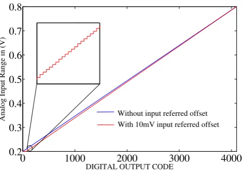
The simulated differential non-linearity (DNL) and inte-gral non-linearity (INL) are shown in Fig. 14. The resultant ENOB is 11.98 bits, which shows that the linearity of this SAR ADC is not affected by the aged buffer circuit. It was confirmed by simulations that also the spectral characteristics of the ADC were not affected. However, the transfer charac-teristics depicted in Fig. 15 shows that a gain error arises in the converter. All SAR ADC’s having resolution (1LSB) value smaller than the worst case input referred offset will be affected by aging degradation in this manner, with mag-nitude depending on the offset. There are proven methods to correct a gain error. But it is important to note that this er-ror will vary over time. Hence special countermeasures need to be implemented to guarantee a stable and correct circuit function for the whole lifetime of the circuit.
7 Conclusions
In this paper a buffer circuit designed in a 32nm high-k, metal gate technology was analyzed by simulation for reliability
Fig. 12. Contribution to Voffset due toVt h shift resulting from NBTI, PBTI and HCI degradation, simulated for stress time of 10 Yrs atVDD=1 V and Temp=85◦C.
6 Impact on ADC performance
To study the impact of an aged buffer circuit on the perfor-mance of a successive approximation ADC circuit, a 12 bit SAR ADC with charge redistribution as illustrated in Fig. 3 was modeled. All the circuit blocks were modeled as ideal elements using Verilog-A to reduce the complexity and the simulation time. A stress induced input referred offset as high as 5mV has been reported for an OTA circuit operated in closed loop configuration (Chouard et al., 2010b). So an input referred offset of 10 mV was assumed as worst case condition for the simulations. The converter was simulated with a clock frequency of 33.33 MHz, and a conversion rate of 1.19 MS/s was used withVrefp=0.8 V,Vrefn=0.2 V and
VDD=1 V.
The simulated differential non-linearity (DNL) and inte-gral non-linearity (INL) are shown in Fig. 14. The resultant
S. More et al.: Reliability Analysis of Buffer Stage 5
P1 N6 N0 P3 N4 N9 P4 N3 N10 P5 N8 N5 P2 N1 N7 P0
−1 −0.8 −0.6 −0.4 −0.2 0 0.2 0.4 0.6 0.8 1
Transistors
Voffset component due to Vth Shift in (V)
BTI Component
HCI Component
Fig. 12. Contribution toVof f set due toVth shift resulting from NBTI, PBTI and HCI degradation, simulated for stress time of 10Yrs atVDD=1V and Temp=85◦C
P1 N6 N0 P3 N4 P4 N9 N3 N10 N8 P5 N5 P2 N1 N7 P0
−0.002 −0.0015 −0.001 −0.0005 0 0.0005 0.001 0.0015 0.002
Transistors
Voffset component due to Id Shift in (V)
HCI Component
NCHCI Component
Fig. 13. Contribution to Vof f set due to Id shift resulting from
HCI and NCHCI degradation, simulated for stress time of 10Yrs atVDD=1V and Temp=85◦C
(±1.09) the difference between theirId shift leads to a
sig-nificant impact onVof f set. The effects of transistorsP2and P3again cancel each other. Comparison of Figs. 12 and 13
shows thatVthshift is the dominant contribution (85.9%) to
Vof f setcompared toIdshift (14.1%).
In summary, the degradation due to circuit aging affects almost all transistors in the buffer circuit. The most de-graded circuit performance isVof f set. Since the OTA in the
buffer circuit always operates in closed loop configuration, its input transistors see smaller stress compared to the output stage transistors. Simulation results show that these output transistors are the main contributors toVof f set. The results
presented here are in-line with experimental findings from (Chouard et al., 2010b).
0 500 1000 1500 2000 2500 3000 3500 4000 4500 −0.1
−0.05 0 0.05 0.1
DIGITAL OUTPUT CODE
INL(LSB)
0 500 1000 1500 2000 2500 3000 3500 4000 4500 −0.1
−0.05 0 0.05 0.1
DNL (LSB)
Fig. 14.Simulated DNL and INL of ADC with 10mV input referred offset in the buffer circuit
6 Impact on ADC Performance
To study the impact of an aged buffer circuit on the perfor-mance of a successive approximation ADC circuit, a 12bit SAR ADC with charge redistribution as illustrated in Fig. 3 was modeled. All the circuit blocks were modeled as ideal elements using Verilog-A to reduce the complexity and the simulation time. A stress induced input referred offset as high as 5mV has been reported for an OTA circuit oper-ated in closed loop configuration (Chouard et al., 2010b). So an input referred offset of 10mV was assumed as worst case condition for the simulations. The converter was simu-lated with a clock frequency of 33.33MHz, and a conversion rate of 1.19MS/s was used withVref p=0.8V,Vref n=0.2V and
VDD=1V.
The simulated differential non-linearity (DNL) and inte-gral non-linearity (INL) are shown in Fig. 14. The resultant ENOB is 11.98 bits, which shows that the linearity of this SAR ADC is not affected by the aged buffer circuit. It was confirmed by simulations that also the spectral characteristics of the ADC were not affected. However, the transfer charac-teristics depicted in Fig. 15 shows that a gain error arises in the converter. All SAR ADC’s having resolution (1LSB) value smaller than the worst case input referred offset will be affected by aging degradation in this manner, with mag-nitude depending on the offset. There are proven methods to correct a gain error. But it is important to note that this er-ror will vary over time. Hence special countermeasures need to be implemented to guarantee a stable and correct circuit function for the whole lifetime of the circuit.
7 Conclusions
In this paper a buffer circuit designed in a 32nm high-k, metal gate technology was analyzed by simulation for reliability
Fig. 13. Contribution to Voffset due to Id shift resulting from HCI and NCHCI degradation, simulated for stress time of 10Yrs atVDD=1 V and Temp=85◦C.
S. More et al.: Reliability Analysis of Buffer Stage 5
P1 N6 N0 P3 N4 N9 P4 N3 N10 P5 N8 N5 P2 N1 N7 P0
−1 −0.8 −0.6 −0.4 −0.2 0 0.2 0.4 0.6 0.8 1
Transistors
Voffset component due to Vth Shift in (V)
BTI Component
HCI Component
Fig. 12. Contribution toVof f set due toVth shift resulting from
NBTI, PBTI and HCI degradation, simulated for stress time of 10Yrs atVDD=1V and Temp=85◦C
P1 N6 N0 P3 N4 P4 N9 N3 N10 N8 P5 N5 P2 N1 N7 P0
−0.002 −0.0015 −0.001 −0.0005 0 0.0005 0.001 0.0015 0.002
Transistors
Voffset component due to Id Shift in (V)
HCI Component
NCHCI Component
Fig. 13. Contribution to Vof f set due to Id shift resulting from HCI and NCHCI degradation, simulated for stress time of 10Yrs atVDD=1V and Temp=85◦C
(±1.09) the difference between theirId shift leads to a
sig-nificant impact onVof f set. The effects of transistorsP2and P3again cancel each other. Comparison of Figs. 12 and 13
shows thatVthshift is the dominant contribution (85.9%) to
Vof f setcompared toIdshift (14.1%).
In summary, the degradation due to circuit aging affects almost all transistors in the buffer circuit. The most de-graded circuit performance isVof f set. Since the OTA in the
buffer circuit always operates in closed loop configuration, its input transistors see smaller stress compared to the output stage transistors. Simulation results show that these output transistors are the main contributors toVof f set. The results
presented here are in-line with experimental findings from (Chouard et al., 2010b).
0 500 1000 1500 2000 2500 3000 3500 4000 4500 −0.1
−0.05 0 0.05 0.1
DIGITAL OUTPUT CODE
INL(LSB)
0 500 1000 1500 2000 2500 3000 3500 4000 4500 −0.1
−0.05 0 0.05 0.1
DNL (LSB)
Fig. 14.Simulated DNL and INL of ADC with 10mV input referred offset in the buffer circuit
6 Impact on ADC Performance
To study the impact of an aged buffer circuit on the perfor-mance of a successive approximation ADC circuit, a 12bit SAR ADC with charge redistribution as illustrated in Fig. 3 was modeled. All the circuit blocks were modeled as ideal elements using Verilog-A to reduce the complexity and the simulation time. A stress induced input referred offset as high as 5mV has been reported for an OTA circuit oper-ated in closed loop configuration (Chouard et al., 2010b). So an input referred offset of 10mV was assumed as worst case condition for the simulations. The converter was simu-lated with a clock frequency of 33.33MHz, and a conversion rate of 1.19MS/s was used withVref p=0.8V,Vref n=0.2V and
VDD=1V.
The simulated differential non-linearity (DNL) and inte-gral non-linearity (INL) are shown in Fig. 14. The resultant ENOB is 11.98 bits, which shows that the linearity of this SAR ADC is not affected by the aged buffer circuit. It was confirmed by simulations that also the spectral characteristics of the ADC were not affected. However, the transfer charac-teristics depicted in Fig. 15 shows that a gain error arises in the converter. All SAR ADC’s having resolution (1LSB) value smaller than the worst case input referred offset will be affected by aging degradation in this manner, with mag-nitude depending on the offset. There are proven methods to correct a gain error. But it is important to note that this er-ror will vary over time. Hence special countermeasures need to be implemented to guarantee a stable and correct circuit function for the whole lifetime of the circuit.
7 Conclusions
In this paper a buffer circuit designed in a 32nm high-k, metal gate technology was analyzed by simulation for reliability
Fig. 14. Simulated DNL and INL of ADC with 10mV input referred
offset in the buffer circuit.
ENOB is 11.98 bits, which shows that the linearity of this SAR ADC is not affected by the aged buffer circuit. It was confirmed by simulations that also the spectral characteristics of the ADC were not affected. However, the transfer charac-teristics depicted in Fig. 15 shows that a gain error arises in the converter. All SAR ADC’s having resolution (1 LSB) value smaller than the worst case input referred offset will be affected by aging degradation in this manner, with mag-nitude depending on the offset. There are proven methods to correct a gain error. But it is important to note that this er-ror will vary over time. Hence special countermeasures need to be implemented to guarantee a stable and correct circuit function for the whole lifetime of the circuit.