Iranian Journal of Electrical and Electronic Engineering, Vol. 15, No. 3, September 2019 310
A Design Methodology for Reliable MRF-Based Logic Gates
S. M. Razavi* and S. M. Razavi*(C.A.)
Abstract: Probabilistic-based methods have been used for designing noise tolerant circuits recently. In these methods, however, there is not any reliability mechanism that is essential for nanometer digital VLSI circuits. In this paper, we propose a novel method for designing reliable probabilistic-based logic gates. The advantage of the proposed method in comparison with previous probabilistic-based methods is its ultra-high reliability. The proposed method benefits from Markov random field (MRF) as a probabilistic framework and triple modular redundancy (TMR) as a reliability mechanism. A NAND gate is used to show the design methodology. The simulation results verify the noise immunity of the proposed MRF-based gate in the presence of noise. In addition, the values from reliability estimation program show the reliability of 0.99999999 and 0.99941316 for transistor failure rates of 0.0001 and 0.001, respectively, which are much better as compared with previous reported MRF-based designs.
Keywords: Reliability, Noise Tolerance, Markov Random Field (MRF), Triple Modular Redundancy (TMR).
1 Introduction1
OISE fluctuation is one of the most important problems in nanometer VLSI circuits [1]. Many noise reduction and noise tolerant techniques have been proposed in the past years. But most of them deal with special types of noise such as power supply noise [2], crosstalk noise [3, 4], dynamic circuits’ noise [5, 6] and substrate noise [7-9]. These methods cannot solve the problem of intrinsic noise in VLSI circuits. Due to the random nature of intrinsic noise, probabilistic-based methods are much better than deterministic ones [10-12].
There are different types of probabilistic approaches. Markov random field (MRF), Bayesian network (BN), probabilistic transfer matrices (PTM) and probabilistic decision diagrams (PDD) are well-known examples. Among these approaches, Markov random field has gained considerable attention for designing noise tolerant VLSI circuits [12-19]. In MRF-based circuits the noise energy is shared among the system
Iranian Journal of Electrical and Electronic Engineering, 2019. Paper first received 17 October 2018 and accepted 14 February 2018. * The authors are with the Faculty of Electrical and Computer Engineering, University of Birjand, Birjand, Iran.
E-mails: [email protected] and [email protected]. Corresponding Author: S. M. Razavi.
components and the noise signal level is reduced noticeably. Therefore, the noise tolerance is achieved. Several MRF-based methods have been used for designing noise tolerant circuits [12-19]. A straightforward method for mapping MRF design principles to VLSI circuits was proposed in [13]. Because of hardware complexity of MRF-based designs, most of the methods which have been proposed focus on techniques of reducing hardware overhead. By valid state reduction through Boolean simplification, a less overhead design in comparison with the straightforward method was proposed in [14]. A master-slave design was proposed by I-Chyn Wey et al. in [12]. They achieved a hardware-efficient design by splitting the truth table into two groups and implemented an MRF-based chip for the 8-bit carry-lookahead adder. A general cost-effective design for logic functions was proposed by Kaikai Liu et al. in [15]. Area-sharing feedback NAND path [16] and global mapping approach [17] are two other methods proposed to reduce the complexity of MRF-based designs. Although the cost-effective methods have the advantage of lower hardware overhead, they usually sacrifice the noise tolerance performance for hardware simplicity. Some methods used special techniques together with hardware simplification to compensate for the degradation of noise tolerance. A noise tolerant logic design based on MRF theory and differential cascade voltage switch
N
Iranian Journal of Electrical and Electronic Engineering, Vol. 15, No. 3, September 2019 311 (DCVS) was proposed in [18]. I-Chyn Wey et al. used
Schmitt trigger circuit to improve the noise tolerance of their cost-effective MRF-based design in [19].
All of the MRF-based designs improve the noise immunity of the VLSI circuits at the expense of hardware overhead. However, using a lot of transistors in a circuit without considering a reliability mechanism deteriorates its reliability. From the well-known general formula Rtn, that Rt is the transistor reliability, the
circuit reliability decreases as the number of transistors (n) increases. This decrease in the reliability can be very serious in today’s nanometer VLSI circuits due to the decline of transistor reliability [1]. Besides manufacturing defects and phenomena such as electromigration, time dependent dielectric breakdown (TDDB) and electrostatic discharge that generally lead to hardware defects, a variety of new reliability concerns have emerged [1, 20]. Negative bias temperature instability (NBTI), positive bias temperature instability (PBTI) and random telegraph noise (RTN) affect modern transistors noticeably and lead to degradation of their electrical properties and timing violations. An unreliable transistor can lead to the failure of the whole MRF-based circuit. Therefore, the efforts for designing noise tolerant circuit will be useless. Taking reliability into consideration makes the MRF-based designs more practical especially in critical applications.
In this paper, we present a reliable MRF-based design methodology for nanometer digital VLSI circuits. The main contribution of this work is the distributed implementation of the MRF-based principles which simple voltage to current and current to voltage converters used as feedback components. Since logic gates are the basic components of digital circuits, a universal NAND gate is chosen to show this design methodology in details. A similar design can be used for other types of gates and standard cell libraries.
The rest of this paper is organized as follows. In Section 2, we explain the reliable MRF-based design methodology in details. Section 3 presents various simulations, reliability evaluations and supplementary discussions to verify the design. Finally, the concluding remarks are in Section 4.
2 Reliable MRF-Based Design Methodology
As the feature size scaled down, the supply voltages of the integrated circuits degraded to 1.2V and lower. In consequence, the noise margin of the circuits decreased. This means that modern circuits are more susceptible to noise compared with traditional ones. Preserving signal to noise ratio (SNR) in the admissible range becomes challenging in nanometer VLSI circuits. Generally, the most important factor in the decline of SNR is intrinsic noise [21]. VLSI circuits suffer from various types of intrinsic noise such as thermal noise, shot noise, etc. To preserve SNR in its allowable range, we should control
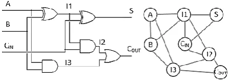
noise by designing noise tolerant circuits. As mentioned before, an appropriate approach is MRF-based design. In an MRF network, each signal can be considered as a node. The state of a node is defined jointly by its neighborhood nodes. Through joint estimation, the noise energy shares between neighbor nodes and the noise level declines noticeably. Fig. 1 shows a full adder circuit and its corresponding MRF network.
In mapping a circuit to an MRF network, nodes that have a logical relationship are fully connected together and form a clique. In this example, nodes A, B and I1 form one clique and totally there are five cliques. To ensure the correct operation of a circuit, the joint probability should remain maximum for all times. From the Hammersley-Clifford theorem the joint probability is obtained from this equation:
1 cc C
U P x
Z kT
(1)In this equation, C is the set of cliques, Uc is the clique
energy function and Z and kT are constants. To keep the joint probability maximum, the clique energy function should remain minimum for each clique. This is minimum in valid states of the corresponding clique. In logic circuits, cliques are correlated with logic gates. Therefore, to ensure maximum joint probability we should enforce the gates to be in their valid states. A common approach is to generate valid states and reinforce them by proper feedback lines. The summation of valid states forms valid states function. Table 1 shows this function for three basic gates. As mentioned before, we introduce our design methodology using NAND gate. A similar approach can be used for other types of gates and standard cell libraries by defining a valid state function for each component.
Consider a two-input NAND gate. The valid states function is F ABC ABC A BC ABC . The simplified form of the function is F ABC ABC . These two terms of the valid states function should be
Fig. 1 A full adder circuit and its corresponding MRF network.
Table 1 Valid states function for basic gates.
Basic Gates Valid States Function (A and B are inputs and C is output)
NOT F AC AC
NAND F ABC ABC A BC ABC NOR F ABC ABC A BC ABC
Iranian Journal of Electrical and Electronic Engineering, Vol. 15, No. 3, September 2019 312 generated and reinforced by proper feedback lines. In
the design procedure, these two points are considered: The complement of each variable in the circuit is
generated as there are only two stable logic states (0, 1) for each variable. We try to force the variables to be in one of their two stable logic states by feedback lines.
Since the terms in the simplified form of the function should be generated and fed back to appropriate nodes, it is probable that the output of the gate has dependency on its previous state. To prevent the circuit to enter such a case, it is better to generate the complements of the terms rather than the noncomplement ones and feed them back to associated nodes.
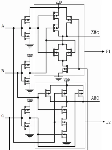
An implementation for the valid states function is
shown in Fig. 2. In this figure, F1 and F2 are ABC and
ABC, respectively. These are the complements of the
terms in the function. A , B and C nodes are used to generate F1 and A, B and C nodes are used to generate F2. It is better to generate F1 and F2 from separate (complement) nodes. By using this technique, each node will have one feedback line and there will be no need for OR gates in the feedback lines.
These valid states should be reinforced by appropriate feedback lines. We propose a novel mechanism for designing feedback lines which is based on distributed TMR [22]. Distributed TMR is a new version of the well-known TMR structure. In this version, the voter unit is omitted and voting is accomplished by voltage to current and current to voltage conversions. In the proposed mechanism simple voltage to current and current to voltage converters are used in a distributed
Fig. 2 An implementation for the valid states function.
TMR structure as feedback components. This technique gives many advantages to the design:
Since the distributed TMR structure is used in an MRF framework, the robust gate will have both noise tolerance and reliability mechanisms.
Adding these converters has a restoring effect on the signals and makes them closer to their ideal noise-free signals.
The converters play the role of isolating elements in the feedback lines. It is essential to isolate output nodes from input ones.
The nodes which the feedback lines should be connected to are shown in Fig. 3. This is the first design for the reliable two-input NAND gate. In this figure, feedback lines are omitted and letters are used to clarify the relationship between the units. Since the TMR structure is used, the central core is repeated three times and the outputs of these cores are connected to the inputs of voltage to current converters. The name of voltage to current converters which are connected to F1 units is C1 and the name of others connected to F2 units is C2. The currents of C1s are added by wiring the outputs of them together. A similar work is done for C2s. The total current of C1s and C2s are given to the inputs of first and second current to voltage converter groups, respectively. We name the converters of the first group B1, B2 and B3 and those of the second group B4, B5 and B6. As we know from distributed voting, majority voting happens in these conversions. Therefore, the output of the first group is the result of voting on F1 generators and the output of the second group is the result of voting on F2 generators.
To reinforce the valid states of the NAND gate, the outputs of the first current to voltage converter group should be connected to the complements of the nodes which constitute F1. The outputs of the second group should be connected to the complements of the nodes which constitute F2. In other words, we connect the outputs of the first group to A, B and Cnodes and the
Fig. 3 The first design for the reliable two-input NAND gate.
Iranian Journal of Electrical and Electronic Engineering, Vol. 15, No. 3, September 2019 313 outputs of the second group to A , B and C nodes.
The simulation results show the noise tolerance of the first design. However, this design can be improved. The outputs of N1 units are connected together to form one node for the feedback line. A similar design exists for N2 and N3 units. If a fault exists or occurs in one of the N1 units and affects the logic value of these units, the output of the whole N1 units will be affected (because the outputs are connected together). This will disrupt the correct operation of the robust gate because the only path for one of the gate’s inputs will be blocked. To resolve this problem, it should be considered that the most important feedback lines are the ones which feedback the output and its complement. The other lines have a low impact on the whole noise tolerance of the gate. The simulation results will verify this statement. If we omit the feedback lines related to the inputs and their complements and repeat the feedback line of the output and its complement for three times and connect them to separated nodes, there will be no need to connect the outputs of similar units together. With this technique, the gate reliability increases considerably.
Fig. 4 shows our main design for the reliable gate. In this design the feedback lines related to the inputs and their complements are omitted completely. Instead, the output and its complement feedback lines are repeated three times. The gate reliability with this design will be evaluated in the next section.
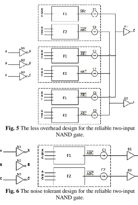
In the main design, distributed implementation is used for the whole structure. However, the hardware overhead of the main design is high and in some applications such a high level of reliability is not essential. We introduce another design for the robust gate with nearly similar noise tolerance (because of the existence of MRF-based design) and lower reliability in comparison with the main design. Fig. 5 shows our third design for the robust gate.
In this design, there are only one group for NOT
Fig. 4 The main design for the reliable two-input NAND gate.
gates and two current to voltage converters for the feedback lines of the output and its complement. The idea behind this design is that the failure probability in bigger units is higher than smaller ones. Therefore, redundancy is utilized only for bigger units in this design.
If the design is only required to be noise tolerant, The TMR structure can be completely removed from the main design. This can lead to a much less overhead design as shown in Fig. 6. The gate with this design has an approximately similar noise tolerance in comparison with the main design. However, there is not any reliability mechanism in this design (like other MRF-based designs). Therefore, if only noise tolerance is important, this design can be used for the gate.
We have proposed four designs for the reliable two-input NAND gate. All of these designs benefit from the novelty of using simple converters as feedback components. The next section presents the simulation results and reliability evaluations for the gate with these designs.
3 Simulation Results, Reliability Evaluations and Supplementary Discussions
All of the simulations in this section were accomplished by Hspice simulation setup with 65nm process technology libraries and 1.2 V supply voltage. The temperature was set to 50 °C to ensure the presence of thermal noise. We pursued worst case circuit analysis to prove the ultra-high reliability and noise immunity of
Fig. 5 The less overhead design for the reliable two-input NAND gate.
Fig. 6 The noise tolerant design for the reliable two-input NAND gate.
Iranian Journal of Electrical and Electronic Engineering, Vol. 15, No. 3, September 2019 314 the proposed designs. This kind of approach ensures the
circuit operation in practical cases in current technologies and future ones which may encounter higher failure rates and lower noise margins. According to this approach, two highly noisy signals were given to the inputs of the reliable two-input NAND gate with various proposed designs. The signals have additive white Gaussian noise (AWGN) -that is the best model for intrinsic noise-, 4dB signal to noise ratio (SNR), 159.9 MHz frequency and different duty cycles. Fig. 7 shows the noisy signals. In this figure, the original signal (before adding noise) is shown, too.
Different duty cycles ensure all four possible combinations of inputs (00, 01, 10 and 11). The 4dB SNR is the lowest signal to noise ratio which has been used for noise tolerance verification in most of the related works and is related to our worst case analysis approach. It is obvious that common deterministic designs cannot tolerate such noisy signals.
3.1 Noise Tolerance Verification
Noisy signals were given to the inputs of the gate with the main design to show its ultra-high noise immunity.
(a)
(b)
Fig. 7 Noisy signals with 4dB SNR: a) Duty cycle 40% and b) Duty cycle 70%.
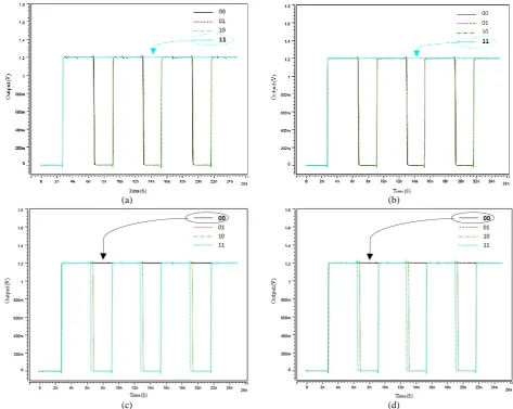
Fig. 8 shows the inputs and output of the gate. According to this figure, the gate operation in the presence of such noisy inputs is ideal. The gate operation with all of the proposed designs in the presence of noisy inputs is shown in Fig. 9. The gate has almost similar output with different designs. It is shown that the gate has ultra-high noise tolerance with all of our proposed designs. However, the difference between these designs is mostly associated with the reliability characteristics.
3.2 Reliability Evaluations in the Presence of Noise
There are various fault sources in the VLSI circuits. Electromigration, time dependent dielectric breakdown (TDDB) and electrostatic discharge are well-known examples of phenomena that generally lead to hardware defects. These defects are usually permanent and can cause the circuit’s output to be in one of the logic states independent of the circuit’s inputs. Negative bias temperature instability (NBTI), positive bias temperature instability (PBTI), hot carrier injection (HCI) and random telegraph noise (RTN) are other
Fig. 8 The output of the gate in the presence of noisy input signals.
Fig. 9 The output of the gate with all proposed designs in the presence of noisy input signals.
Iranian Journal of Electrical and Electronic Engineering, Vol. 15, No. 3, September 2019 315 phenomena that affect modern transistors greatly and
lead to timing violations. Threshold voltage and drain current fluctuations are the main reasons for timing violations that can cause the circuit’s output to get into an unknown state ‘X’. This means that the output would be either 1 or 0 independent of the inputs. In addition, there are transient faults that temporarily flip a logic state. These faults can also alter the output of the circuit to an unknown state.
A precise reliability evaluation requires an appropriate fault model. We define a fault model based on a macroscopic view.
3.2.1 The Fault Model
Consider the main design (Fig. 4) again. This design is organized from different units (F1 and F2 generators, converters and NOT gates). The following assumptions are considered in the fault model:
If a fault exists or occurs in a special unit, the whole unit will be assumed to be faulty (worst case assumption).
The faulty unit reveals its failure in one of the two potential forms. In the first form, the logic value of the unit’s output is 1 regardless of its inputs and in the second form, the logic value of the unit’s output is 0 regardless of its inputs. Of course, for voltage to current converters the meanings of these two forms are maximum current and zero current (that is equal to a high impedance node) in order.
3.2.2 Reliability Evaluation
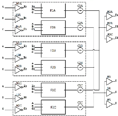
Consider Fig. 10. In this figure the labels of the different units in the main design are changed for simplicity in reliability evaluation. All of these labels (except for current to voltage converters which are directly connected to the output) have three parts:
The first part shows the name of that unit. N, F, C and B letters show NOT gates, generators, voltage to current converters and current to voltage converters in order. Letter L also shows NOT gate.
The second part shows the artery in which a unit exists. In this design there are two arteries and each one has three paths. The reason for two arteries is that there are two terms in the simplified form of the valid states function in the two-input NAND gate. The third part introduces the group which a unit
belongs to. In this case there are three groups (A, B and C) because we used TMR (3MR) structure in our design. These groups are separated from each other by dotted rectangular.
Current to voltage converters which are connected directly to the output node cannot be categorized in a specific artery or group. Therefore, their labels only show their names.
Each unit in this design repeats three times (since there is a TMR structure). Therefore, in the following conditions the gate will operate correctly:
If a specific unit fails to work.
If several units which exist in one path from a certain artery fail to work.
If several units in two paths from different arteries fail to work.
If several units that belong to a specific group (A, B and C) fail to work.
However, if failed units belong to two paths from one artery or two current to voltage converters from the B3, B4 and B5 group, the gate will lose its correct operation in certain states. To find these certain states that cause the robust gate to fail, we inquired the mentioned condition for all units in the gate. For each specific unit (N, F and …), one pair was selected. Then the inputs of this pair were separated from the main circuit and were connected to VDD or GND to adjust the outputs of the pair to one of four possible combinations 00, 01, 10, 11. For the outputs of the voltage to current converters, 0 and 1 mean zero current and maximum current, respectively.
The simulations which show the tests results are presented in this subsection. In all of the tests, there were noisy signals on the gate’s inputs. The pairs which were selected for the tests are from A and B groups. Obviously, because of similarity in the circuit characteristics, these results are valid for pairs from A and C and also B and C. Fig. 11 shows the tests results of the units which exist in the first artery (N1, L1, F1 and C1 units).
As shown in Fig. 11, in all of these tests, only in the case of one combination from the four possible combinations the gate loses its correct functionality. This combination is bolded in the figures. Therefore, if one pair from a unit in the first artery goes out of work, the whole of the gate will fail to work with a probability of 25%. The simulation results related to the units which exist in the second artery are shown in Fig. 12.
Fig. 12 shows that in the second artery the probability of failure depends on the units. There are
Fig. 10 The main design with changed labels.
Iranian Journal of Electrical and Electronic Engineering, Vol. 15, No. 3, September 2019 316
(a) (b)
(c) (d)
Fig. 11 The tests results of the units in the first artery: a) N1A and N1B units, b) L1A and L1B units, c) F1A and F1B units, and d) C1A and C1B units.
three different probabilities for the gate failure. If one pair from N2 units fails to work, the probability of failure will be zero and for a pair from B2 units it will be 0.25. Otherwise, this probability will be 0.5. The reliability evaluation is based on choosing a pair from each of several distinct units, therefore we will omit N2 units from our reliability calculations because for each pair, the gate will keep its correct functionality. Indeed, we can completely remove N2 units from the design as they only have a little positive impact on noise tolerance and no impact on correct functionality. This can reduce the hardware cost by 6 transistors (3 NOTs). The last group is B3, B4 and B5 units. Fig. 13shows the result of the test on these units. It is obvious that in half of the combinations, the gate will operate correctly.
In all of these tests, units that failed to work were in two paths from one artery or in two current to voltage converters from the B3, B4 and B5 group. It is obvious that if these units belong to more than two paths from one artery or more than two converters from this group, the gate will fail to work.
3.3 Reliability Analysis
Considering the mentioned topics, we can now propose an algorithm to estimate the gate reliability. The algorithm is as follows:
First step: for a given failure rate, we inject F×TC
faults into the circuit randomly. In other words, a number of F×TC transistors are selected randomly to
be faulty in each run. TC is the number of transistors
in the circuit and F is the failure rate. Each unit which has faulty transistors will fail to work according to the mentioned fault model.
Second step: the failed units are compared with each other mutually. If two failed units exist in two paths from the second artery or in the B3, B4 and B5 group, we add 0.5 to a variable S; else if they exist in two paths from the first artery, we add 0.25 to the S. If the failed units belong to more than two paths from one artery or more than two converters from the mentioned group, we add 1 to the S. The variable S with initial value of 0 shows summation of failure probabilities in the gate.
Third step: we repeat prior steps in a Monte Carlo
Iranian Journal of Electrical and Electronic Engineering, Vol. 15, No. 3, September 2019 317
(a) (b)
(c) (d)
Fig. 12 The tests results of the units in the second artery: a) N2A and N2B units, b) F2A and F2B units, c) C2A and C2B units, and d) B2A and B2B units.
process with uniform distribution. In high levels of repetition, reliability of the robust gate is calculated
from the following equation: R 1 S
N
. In this equation, N is the number of repetitions and R is the gate reliability. The results of the reliability estimation program were obtained in one hundred million repetitions.
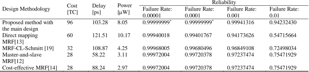
The circuit metrics of the proposed gate and the major previous reported MRF-based 2-input NAND gates are provided in Table 2. As there is not any Reliability mechanism in the previous MRF-based designs, their reliabilities were calculated byRtn
formula. In this formula, Rt shows transistor reliability
and n represents the number of transistors. The results demonstrate that the reliability of our proposed gate is much higher than other noise tolerant MRF-based gates in the wide range of failure rates and at the same time the proposed gate demonstrates acceptable cost, delay and power. For the failure rates of 0.00001 and 0.0001, the program returns 1 for the reliability. It means that in
one hundred million repetitions there is not any state which falls into the aforementioned conditions for the gate failure. This is a valuable result especially when considering that the reliability evaluations were performed in the worst case analysis platform. Although the program returns 1 for the reliability in these failure rates, we insert 0.99999999 instead of 1 in the table because it is a more appropriate number for reliability.
3.4 Power, Delay and Cost Discussions
Power: The power consumption of a circuit is proportional to the square of supply voltage. Therefore, lowering the supply voltage has a great impact on power consumption. It is mathematically proven [23] that under the same output correct probability, the MRF-based circuits can operate with lower supply voltage in comparison with the traditional ones. This valuable feature can compensate for the power consumption which is imposed on the circuit due to transistor count. Moreover, due to lower voltage swing in distributed voting [22], the converters part of the proposed gate consume less power and consequently the overall power
Iranian Journal of Electrical and Electronic Engineering, Vol. 15, No. 3, September 2019 318 Fig. 13 The test result of the B3, B4 and B5 group.
Table 2 Circuit metrics of MRF-based two-input NAND gates with different design methodologies.
Design Methodology Cost [TC]
Delay [ps]
Power [W]
Reliability Failure Rate:
0.00001
Failure Rate: 0.0001
Failure Rate: 0.001
Failure Rate: 0.01 Proposed method with
the main design
96 103.28 8.05 0.99999999* 0.99999999* 0.99941316 0.94232430
Direct mapping MRF[13]
60 121.51 10.17 0.99940018 0.99401767 0.94173626 0.54715664
MRF-CL-Schmitt [19] 32 108.87 4.25 0.99968005 0.99680496 0.96849108 0.72498034 Master-and-slave
MRF[12]
28 58.22 3.11 0.99972004 0.99720378 0.97237474 0.75471929
Cost-effective MRF[14] 28 88.24 2.97 0.99972004 0.99720378 0.97237474 0.75471929
* The program returns 1 for the reliability in this failure rate.
consumption is competent as shown in Table 2. The supply voltage of the proposed reliable gate can be set to a near threshold value without any concern for the decrease in the noise margin, because the proposed design ensures ultra-high noise immunity. The optimum number for the supply voltage is application dependent, however, it can range from nominal value to near threshold values.
Delay: The propagation delay of the MRF-based circuits is bigger than that of the traditional ones, but MRF-based circuits can achieve similar transition time [24]. Considering transistor count in various MRF-based circuits in table 2 shows that the proposed design methodology requires more transistor in comparison with others. However, most of these transistors used in parallel because of TMR structure and do not participate in the critical path between inputs and output and consequently do not affect the propagation delay. Cost: John von Neumann et al. introduced the idea of using redundancy to achieve reliable organisms from unreliable components for the first time [25]. From that time, redundancy has been considered as a major strategy in designing highly reliable systems and widely used in many applications. In another fundamental research [26], the economic constraints of redundancy factor (the number of times which a computing unit is replicated) was investigated. It was reported that the redundancy factor R is small or economical when R ≤ 100 and is very small or practical when R ≤ 10. It
shows that even up to one hundred repetitions of a computing unit can be considered in reliability oriented researches. Among our proposed designs, the main design which is the most redundant one has only the redundancy factor of R = 3 for all of the components. This redundancy factor leads to more hardware overhead (transistor count of 96) in comparison with other MRF-based circuits, however, we achieve incomparable reliability.
4 Conclusion
Designing MRF-based noise tolerant circuits without considering reliability concerns will not be an appropriate method for nanometer VLSI circuits. We took reliability into consideration in MRF-based designing and defined a new methodology that leads to highly reliable components. We proposed multiple designs with different levels of hardware overhead. The simulations and reliability evaluations confirmed ultra-high reliability and noise immunity of the proposed method.
References
[1] Semiconductor Industry Association, “The
international technology roadmap for
semiconductors 2.0 – More Moore,” 2015 Edition. [Online]. Available: http://www.itrs2.net/itrs-reports.html.
Iranian Journal of Electrical and Electronic Engineering, Vol. 15, No. 3, September 2019 319 [2] E. Bohannon, C. Urban, M. Pude, Y. Nishi,
A. Gopalan, and P.R. Mukund, “Passive and active reduction techniques for on-chip high-frequency digital power supply noise,” IEEE Transactions on
Very Large Scale Integration (VLSI) Systems,
Vol. 18, No. 1, pp. 157–161, Jan. 2010.
[3] S. Singh and V.S. Verma, “Reduction of crosstalk noise and delay in VLSI interconnects using schmitt trigger as a buffer and wire sizing,” in Advances in Computing and Information Technology, Vol. 178, pp. 677–686, 2013.
[4] C. Lin and H. Zhou, “Tradeoff between latch and flop for min-period sequential circuit designs with crosstalk,” IEEE Transactions on Computer-Aided Design of Integrated Circuits and Systems, Vol. 26, No. 7, pp. 1222–1232, Jul. 2007.
[5] L. Ding and P. Mazumder, “On circuit techniques to improve noise immunity of CMOS dynamic logic,” IEEE Transactions on Very Large Scale Integration (VLSI) Systems, Vol. 12, No. 9, pp. 910– 925, Sep. 2004.
[6] I. C. Wey, Y.G. Chen, and A. Y. Wu, “Design and analysis of isolated noise-tolerant (INT) technique in dynamic CMOS circuits,” IEEE Transactions on
Very Large Scale Integration (VLSI) Systems,
Vol. 16, No. 12, pp. 1708–1712, Dec. 2008.
[7] M. S. Peng and H. S. Lee, “Study of substrate noise and techniques for minimization,” IEEE Journal of Solid-State Circuits, Vol. 39, No. 11, pp. 2080– 2086, Nov. 2004.
[8] C. Liu, X. Wang, C. Wang, L. Han and J. Wang, “Substrate Noise Suppression Method Analysis of Integrated Circuit,” in International Conference on Optoelectronics and Microelectronics (ICOM),
Changchun, China, 2015.
[9] S. Uemura, Y. Hiraoka, T. Kai, and S. Dosho, “Isolation techniques against substrate noise coupling utilizing through silicon via (TSV) process for RF/mixed-signal SoCs,” IEEE Journal of Solid-State Circuits, Vol. 47, No. 4, pp. 810–816, Apr. 2012.
[10]K. Nepal, R.I. Bahar, J. Mundy, W.R. Patterson and A. Zaslavsky, “Designing logic circuits for probabilistic computation in the presence of noise,” in Proceedings of the 42nd Design Automation
Conference, Anaheim, CA, USA, 2005.
[11]J. Chen, J. Mundy, Y. Bai, S. C. Chan, P. Petrica, and R. I. Bahar, “A probabilistic approach to nano-computing,” in IEEE non-silicon computer
workshop, San Diego, CA, USA, 2003.
[12]I. C. Wey, Y. G. Chen, C. H. Yu, J. Chen and A. Y. Wu, “Design and implementation of cost-effective probabilistic-based noise tolerant VLSI circuits,” IEEE Transactions on Circuits and Systems I: Regular Papers, Vol. 56, No. 11, pp. 2411–2424, Nov. 2009.
[13]I. C. Wey, Y. G. Chen, C. H. Yu, J. Chen, and A. Y. Wu, “A 0.18 μm probabilistic-based noise-tolerate circuit design and implementation with 28.7 dB noise-immunity improvement,” in IEEE Asian Solid-State Circuits Conference, Hangzhou, China, 2006.
[14]K. Nepal, R. I. Bahar, J. Mundy, W. R. Patterson, and A. Zaslavsky, “Optimizing noise-immune nanoscale circuits using principles of Markov random fields,” in Proceedings of the 16th ACM
Great Lakes Symposium on VLSI, Philadelphia, PA,
USA, 2006.
[15]K. Liu, T. An, H. Cai, L. Naviner, J. F. Naviner, and H. Petit, “A general cost-effective design structure for probabilistic-based noise-tolerant logic functions in nanometer CMOS technology,” in IEEE
EuroCon, Zagreb, Croatia, 2013.
[16]Y. Li, X. Li, J. Hu, and S. Yang, “Area-sharing cyclic structure MRF cirucits design in ultra-low supply voltage,” in IEEE International Symposium on Circuits and Systems (ISCAS), Lisbon, Portugal, 2015.
[17]Y. Li, I. S. Member, J. Hu and I. Member, “Extensional Design for Noise-Tolerate MRF Standard Cells via Global Mapping,” in IEEE International Symposium on Circuits and Systems
(ISCAS), Melbourne VIC, Australia, 2014.
[18]X. Yang, F. Qiao, Q. Wei and H. Yang, “A General Scheme for Noise-Tolerant Logic Design Based on Probabilistic and DCVS Approaches,” in IEEE 13th
International New Circuits and Systems Conference
(NEWCAS), Grenoble, France, 2015.
[19]I. C. Wey and Y. J. Shen, “Hardware-efficient
common-feedback Markov-random-field
probabilistic-based noise-tolerant VLSI circuits,”
Integration, the VLSI Journal, Vol. 47, No. 4, pp. 431–442, Sep. 2014.
[20]S. Kundu and A. Sreedhar, Nanoscale CMOS VLSI Circuits (Design for Manufacturability). Mc Graw Hill, 2010.
[21]H. Song, VLSI Noise Processing Circuits-Theoretical Bases and Implementations. Hongjiang Song, 2018.
Iranian Journal of Electrical and Electronic Engineering, Vol. 15, No. 3, September 2019 320 [22]A. Namazi and M. Nourani, “Gate-level
redundancy: A new design-for-reliability paradigm for nanotechnologies,” IEEE Transactions on Very Large Scale Integration (VLSI) Systems, Vol. 18, No. 5, pp. 775–786, May 2010.
[23]Y. Li, J. Hu and Y. Li, “Supply voltage analysis for MRF circuits design based on information theory,”
IEICE Electronics Express, Vol. 14, No. 1, pp. 1–8, 2017.
[24]W. Jian, Y. Sheng and H. Jian-hao, “Timing performance for MRF-based circuits with low supply voltage,” in International Conference on
Integrated Circuits and Microsystems (ICICM),
Chengdu, China, 2016.
[25]J. V. Neumann, C. E. Shannon, and J. McCarthy, “Probabilistic logics and the synthesis of reliable organisms from unreliable components,” in
Automata Studies (Annals of Mathematics Studies), Princeton Univ. Press, pp. 43–98, 1956.
[26]S. Roy and V. Beiu, “Majority multiplexing-economical redundant fault-tolerant designs for nanoarchitectures,” IEEE Transactions on
Nanotechnology, Vol. 4, No. 4, pp. 441–451,
Jul. 2005.
S. M. Razavi received the M.Sc. degree from Iran University of Science and Technology (IUST), Tehran, Iran. He has been working toward the Ph.D. degree in Faculty of Electrical and Computer Engineering, University of Birjand, Birjand, Iran. His research interests include design for reliability, fault tolerance in digital VLSI circuits and computer architecture.
S. M. Razavi received the M.Sc. and Ph.D. degrees from Tarbiat Modarres University, Tehran, Iran. He has been a Faculty Member at the University of Birjand, Birjand, Iran, where he is currently an Associate Professor of Electrical Engineering. His research interests include computer architecture and pattern recognition.
© 2019 by the authors. Licensee IUST, Tehran, Iran. This article is an open access article distributed under the terms and conditions of the Creative Commons Attribution-NonCommercial 4.0 International (CC BY-NC 4.0) license (https://creativecommons.org/licenses/by-nc/4.0/).