Vol. 48, No. 1, Spring 2016, pp. 53- 61 )AIJ-EEE)
٭
Corresponding Author, Email: [email protected]
Time-Mode Signal Quantization for Use in Sigma-Delta
Modulators
M. Tamaddon
1and M. Yavari
2*1- PhD. Student, IC Design LAB, Dep. of Electrical Engineering, Amirkabir University of Technology, Tehran, Iran. 2- Associate Professor, IC Design LAB, Dep. of Electrical Engineering, Amirkabir University of Technology, Tehran, Iran.
Received August 11, 2015, Accepted November 12, 2015
ABSTRACT
The rapid scaling in modern CMOS technology has motivated the researchers to design new
analog-to-digital converter (ADC) architectures that can properly work in lower supply voltage. An exchanging the
data quantization procedure from the amplitude to the time domain, can be a promising alternative well adapt
with the technology scaling. This paper is going to review the recent development in time-based
noise-shaping ADCs, so-called as time-based sigma-delta modulators. Two of the most important architectures
named as voltage-controlled oscillator (VCO) -based and time-to-digital (TDC) -based sigma-delta
modulators (SDMs) are selected to be reviewed in this paper. The intrinsic advantages and limitations of
these structures are briefly explored. To confirm the effectiveness of the time-mode sigma-delta modulators,
a TDC-based continuous-time sigma-delta modulator is proposed as an example and the related simulation
results performed in MATLAB are illustrated.
The simulation results show that the proposed modulator achieves a dynamic range of 67 dB over 30 MHz with the loop filter of order 2.The proposed TDC-based sigma-delta
modulator shows the superiority of the time quantization approach in designing the wideband and less
complex continuous-time SDMs.
KEYWORDS
1- INTRODUCTION
The advance of CMOS technologies has resulted in restricting the voltage headroom of the circuits. As a consequence, the performance of voltage-based mixed-mode circuits scales poorly with technology. Nevertheless, the scaling, has led to the significant improvement in the time accuracy of digital circuits. In the time mode approach the analog variables are represented by the time information rather than the nodal voltages or branch currents. Improvement of the time accuracy, due to the technology scaling offers an attractive and technology-friendly alternative for conventional amplitude-mode signal processing. Analog-to-digital converters (ADCs) are the key components of mixed-mode systems which can be benefited from this superiority [1].
Time-mode circuits possess a number of intrinsic characteristics that are scaled well with CMOS technology, making them a promising and viable option to implement some of the key building blocks of mixed analog-digital subsystems such as ADCs and Phase-Locked Loops (PLLs). Among the time-based ADCs, time-to-digital converter (TDC) and voltage-controlled-oscillator (VCO) -based ADCs have emerged as attractive solutions due to their highly digital intensive circuit architecture [2].
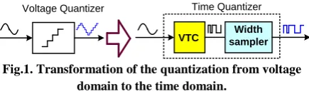
Voltage Quantizer
VTC
Time Quantizer
Width sampler
Fig.1. Transformation of the quantization from voltage domain to the time domain.
Sigma-delta modulators (SDMs) have attracted a lot of attention as a digital friendly structure for ADCs because the substantial part of the signal processing is performed in digital domain [3, 4]. By using the time-based signal processing approach, the shortcomings (i.e., higher power consumption, higher mismatches and etc.) related to the key component of the sigma-delta modulators can be significantly resolved. As is shown in Fig. 1, in the time-mode signal processing, an input voltage or the current is converted to a time variable using a voltage-to-time converter (VTC). The VTC can be realized using VCOs [5], PWMs [6], or voltage controlled delay units (VCDUs) [1]. The resultant time variable is then quantized using a width sampler such as time-to-digital converter (TDC) or a counter.
Architecturally, time-mode ADCs can be classified into the open-loop and closed-loop structures. Although the open loop time-mode ADCs can have short
conversion time and lower power consumption, however, their performance is severely affected by the nonlinearity of the VTC and non-ideality of the sampler. In contrast, the closed-loop topology employs the negative feedback to improve the performance of the ADC.
Iwata et al. [7] showed that an input voltage can be multi-bit quantized using a multi-stage voltage-controlled ring oscillator in series with a counter. The TDC-based sigma-delta modulator is another type of time-mode ADCs. In this structure, the conventional quantizer is realized with the combination of a VTC and a multi-bit TDC. The TDC produces the digitized version of the pulse width. Unlike the VCO-based quantizers, where the inherent first order noise shaping is obtained without any feedback, the TDC-based quantizers do not have this feature. Thus, it is not usual to utilize the TDC-base quantizer in an open structure unless the lower resolution is needed.
This paper is organized as follows. In Sect. 2 an overview of the VCO-based quantizer is provided with highlighting their most important features. In Sect.3, TDC-based quantizer is introduced. A table for the sake of the comparison of several time-based ADCs is presented in this section. As a design example a TDC-based continuous-time sigma-delta modulator is proposed in Sect. 4, to show the effectiveness of the time quantization approach. Finally, Sect. 5 concludes the paper.
2- VCO-BASED QUANTIZATION
counter clock rate can be lower than the VCO maximum frequency in the event that, the criteria fs>2*fmax should be satisfied in the frequency-mode VCO-based ADC. The phase-mode block diagram of the VCO-based ADC followed by its linearized model is illustrated in Fig. 2. Since the phase of the VCO is ideally proportional to its control voltage, the number of the cycles of the VCO in one sampling period Ts yields the digital representation of the sampled input voltage. Also, the frequency-mode one is shown in Fig. 3. As is clear, The VCO-based ADC typically consists of a sample-and-hold (S/H), a multi-stage ring VCO (RVCO), and a digitizer. The input is sampled and held by the S/H block and used to control the VCO.
Regarding that the VCO can be linearly modeled as an integrator [8], it can be shown that the output signal of phase-mode VCO-based ADC representing in z-domain is:
-1
1
( )
[
( ) (1-
) ( ) ]
2
out VCO in
D
z
K
V
z
z
E z
(1)where Vin is the input signal, E(z) is the z-transform of the error signal and Kvco is the conversion gain of the VCO.
Identical to the phase-mode one, the output signal of the frequency-mode VCO-based ADC can be stated as:
-1
( )
( ) (1-
) ( )
out VCO in
D
z
K
V z
z
E z
(2)The form of the output signal in (1) and (2) reveals that the quantization noise, E(z), is high-pass filtered and thus the first-order noise shaping is achieved. Thus this ADC can be classified as a sigma-delta modulator. It is worth noting that this superiority is obtained without any feedback loop or an extra amplifier. The equivalent number of the bits associated with the VCO-based sigma-delta modulator can be calculated from [9]:
2
log
ph tunebit s
N
f
n
f
(3)where ftune is the frequency tuning range of the VCO, and Nph is the number of the phases of the VCO which are involved in the quantization process. From (3) and according to the linear model, the SNR of the VCO-based can be derived as [9]:
20log
tune ph30log
- 3.41
dB s
f
N
SNR
OSR
f
(4)S/H RVCO Counter
fs fs
[ ]k
[ ]
in V k in
V Dout
( ) in V z ( ) E z ( ) D z 1 1 VCO K z 1 1 2 z Phase quantizer (a) (b)
( )z
Fig. 2. Phase-mode VCO-based ADC, (a) the block diagram, (b) its linearized z-domain model [2].
Phase differentiator ( ) in V z ( ) E z ( ) D z 1 1 VCO K z 1 1 z (b)
( )z
D Q Clk D Q Clk [ ] in V k D Q Clk D Q Clk D Q Clk D Q Clk fs out D RVCO S/H fs in V (a) fs fs
Fig. 3. Frequency-mode VCO-based ADC, (a) the block diagram,(b) its linearized model [7].
where, OSR is the oversampling ratio and is defined as fs/2fBWand fBWis the signal bandwidth. It implies that, as the number of the VCO phases increases (i.e., the multi-phase VCO-based ADC) the resolution of the modulator is enhanced.
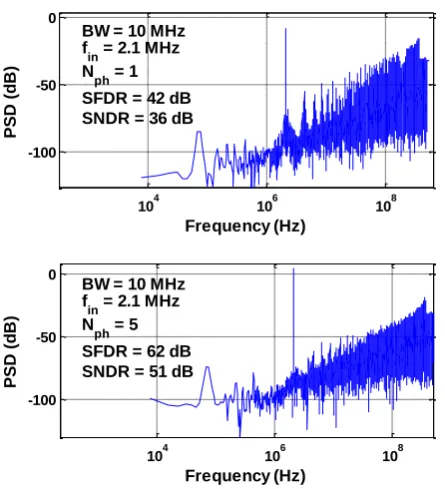
This feature is more clarified through the system-level simulation of the modulator for two different cases (Nph=1 and Nph=5) as shown in Fig. 4. In this simulation, a differential frequency-mode VCO-based ADC is selected as a case study. The input signal is a sinusoidal one with an amplitude of 0.1 V, the sampling frequency is fs=1 GHz and the KVCO=1.5 GHz/V while the VCO center frequency is chosen as f0=300 MHz.
can be made sufficiently large. As a result, large OSRs can be considered for these ADCs.
Fig. 4. Simulation results of a VCO-based ADC for the input signal amplitude of 0.1 V.
However, the performance of the VCO-based ADC is deteriorated by the nonlinear voltage-to-phase characteristic of the VCO. This adverse effect gets more severe when the variation of the input voltage is large. An intensive effort has been introduced in compensating this bottleneck while preserving the positive features of the VCO-based quantizers.
In [10], a VCO-based multi-bit quantizer is employed inside a continuous-time ΔΣ loop. This design partially solves the nonlinearity error of the VCO while generating implicit dynamic element matching of the feedback digital-to-analog converter (DAC) elements. Although the feedback loop serves to suppress VCO nonlinearity and phase noise, the signal-to-noise-plus distortion ratio (SNDR) of the overall ADC is still limited by VCO nonlinearity. In [11], a VCO-based quantizer is used along with a feedback DAC to linearize the VCO by reducing its input swing. In [12], four VCOs are used along with digital calibration to reduce the effects of VCO nonlinearity. The approach proposed in [13], the pulse width modulation (PWM) prior to the VCO forces the VCO to toggle between two frequencies, flow and fhigh. This way, the VCO operates linearly to improve the overall SNDR of the ADC. However, the nonlinearity of the PWM block can be a new problem needs to be cared. In [14], a multi-rated multi-stage structure for the sigma-delta modulator is proposed where the first stage is a conventional first order modulator, while the second
stage is a VCO-based sigma-delta modulator. The control voltage of the VCO is the error signal generated in the first stage. Using this scheme, the nonlinearity of the VCO is significantly suppressed, since its input has a small swing.
3- TDC-BASED QUANTIZATION
TDCs convert a time-difference variable to a digital code. The use of TDCs in nuclear science research dates back to 1970s. The applications of TDCs, however, has extended well beyond nuclear science to digital storage oscillators, laser range finders , digital frequency synthesizers, and ADCs, to name a few [15, 16]. TDC-based sigma-delta modulators are another structures classified as time-mode ADCs. Here, the width of the pulses generated by a preceding VTC is quantized with the time resolution of TQ.
In [17], a closed-loop continuous-time (CT) sigma-delta modulator employing a synchronous ramp-based pulse-width modulator (PWM) as the VTC and a multi-bit flash TDC as the sampler is introduced. Although some significant achievements are reported, this architecture suffers from some main problems mainly arising from the nonlinearity of synchronous PWM. In frequency domain, the synchronous ramp-based PWM waveform’s spectrum contains the signal frequency, reference frequency and its harmonics and progressively higher order intermodulation products of the reference harmonics and signal frequency. The feedback pulse generated by the TDC is a sampled and held version of the PWM pulse with a sampling period of TQ. This sampling process results in aliasing of the high frequency tones within the spectrum of the input PWM waveform. Hence, the noise floor is significantly increased resulting in the degradation of the modulator performance. The time-encoded structures in [18, 19] can also be categorized into wideband high performance PWM-based CT sigma-delta modulators. However, their sampling rates are in the order of multi-GHz resulting in significant power consumption in the quantizer. As a design example, a CT TDC-based sigma delta modulator is explored in the following section.
Table. 1 compares the performance of some recent work in time-based ADCs implemented in CMOS technology.
104 106 108 -100
-50 0
Frequency (Hz)
PSD
(d
B
)
104 106 108 -100
-50 0
Frequency (Hz)
PSD
(d
B
)
BW = 10 MHz fin = 2.1 MHz Nph = 1 SFDR = 42 dB SNDR = 36 dB
BW = 10 MHz f
in = 2.1 MHz
TABLE 1
PERFORMANCE COMPARISON OF TIME-MODE ADCS
Ref. Tech
(nm) fs
(MHz) BW (MHz)
SNDR (dB)
Power (mW)
FoM (fJ/step) [20]
TCAS.I' 09 180 140 0.4 38.2 0.8 14381
[21]
VLSI Symp.' 07
130 950 20 55 38.4 2089
[22]
ISCAS' 09 130 900 20 78 87 331
[23]
CICC' 11 130 1200 4 77 13.8 298
[24]
ISSCC' 09 65 250 20 60 10.5 321
[25]
IEEE Conf.' 12
90 560 20 67.3 3.1 40.6
[26]
TVLSI' 12 130 600 20 52.5 14.3 1043.8
[13]
VLSI Symp.' 11
180 10 0.5 66 0.475 285.5
[27]
IEEE MTT-S' 11
90 640 8 59 4.3 341.2
[28]
ESSCIRC'
06
90 3.4 0.02 44.2 0.044 5670
[29]
JSSC' 11 65 1200 600 20.4 2 104.2
4- PROPOSED DESIGN EXAMPLE
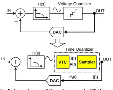
In order to further emphasize the superiority of the time-based encoding, the concept is elaborated for a TDC-based continuous-time sigma-delta modulator. The conceptual block diagram of the proposed modulator is depicted in Fig. 5. It shows how a conventional SDM is exchanged to a time-based one.
DAC H(s)
IN OUT
VTC Sampler
Time Quantizer DAC
Voltage Quantizer H(s)
IN OUT
P(t)
Pq(t)
Fig. 5. An exchange of the voltage-mode CT sigma delta modulator to the time-mode one.
For the proposed time-based continuous-time modulator (TCSDM), an asynchronous PWM (APWM) is utilized as a VTC. The structure of the APWM is illustrated in Fig. 6. An APWM is similar to a single-bit sigma-delta modulator. It is a closed-loop nonlinear system, transforms the information in the amplitude axis into the time axis. An APWM consists of an integrator, a
hysteretic comparator, and a negative feedback loop. In the APWM loop, A(s) represents a first order passive low-pass filer (LPF) and the comparator is a hysteretic one with the hysteresis factor of h. The hysteretic comparator is inherently a nonlinear positive feedback circuit which can be quasi-linearly modeled using describing functions (DFs) [30]. The nonlinearity of the comparator is denoted as N(A,φ). APWM oscillates at the carrier frequency of fc for a zero input signal. Applying the Barkhausen oscillation criterion for a zero input, the limit cycle and its amplitude will be obtained by solving of the following equation:
-1/N A,
A j
@
c (5)Equation (5) can be solved graphically to find the value of the limit cycle frequency where the limit cycle can be determined from the crossing point of the -1/N(A,φ) and A(jω) curves. Assuming a first order A(s) as ωa/(s+ωa) the self oscillation frequency, fc is obtained as:
2 2
2 4 - 4
a
a c
h
h h
(6)
( , ) N A
DAC
v(t) r(t) i(t) p(t)
A(s)
-h
D
h
h
Fig. 6. The block diagram of an APWM.
The oscillation frequency or a limit cycle denoted by fc is the main design parameter that determines the spectral purity and the quality of the amplitude-to-time transformation. The spectral properties of the APWM can be determined through an analysis of limit cycle oscillations.
Pq(t)
EQ(t) P(t)
TQ
Fig. 7. Quantization of the pulse widths by a time-based sampler.
In an APWM, the output signal is a lossless representation of its input, since the information is stored in the pulse width. However, the sampling will introduce an error even if the sampling frequency is higher than the Nyquist rate. The average rate of the error occurrence is f0
for a non-zero sinusoidal input signal. The power spectral density (PSD) of EQ(t) is needed to calculate the quantization noise effect of the sampler. However, it is difficult to make an exact analysis due to the redundancy of the error pulse widths. But fortunately, this is not really necessary to find an exact mathematical formula for this purpose [31]. For a sampler with the resolution of TQ, the error signal, is approximated as:
0
-- ; - 2 2
n Q n Q
n
e t Q
t nT T Q T
(7)where Qn is the amplitude of the error pulses and T0 is
the inverse of the instantaneous frequency of the APWM (T0=1/f0). Hence, a rough approximation of the error
single-sided PSD is given in [31] as:
2 0
0 8 3 e
Q
f
S f
f f
(8)
where Se(f) is the approximated PSD of the error
signal and fQ is the virtual sampling rate of the time-based
sampler (i.e., fQ=1/TQ).
For an APWM oscillating at the limit cycle of fc, the output signal of the filter, H(s), is sampled with the frequency of fc rather than fs. This means that the loop does not have to handle the sample frequency but only the oscillation frequency, fc. As a result, a new parameter
named as over-cycling ratio (OCR) is utilized instead of a well-known oversampling ratio (OSR) in the proposed TCSDM. The OCR is defined as fc/2fB where fB is the signal bandwidth. The approximated signal-to-noise ratio
of the TCSDM based on the APWM which utilizes a resonator-based LPF for H(s), is stated as [32]:
(9)
where, Up is the input signal amplitude and L is the order of the filter, H(s).
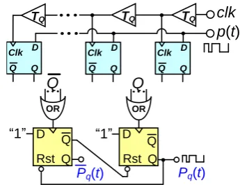
For an APWM the minimum required sampling frequency, fQ for the proper detection of the pulse edges is four times the fc [32]. For wideband TCSDMs a higher fc is required, giving rise to the minimum required value of fQ, (e.g., multi-GHz). A poly-phase sampler can be a suitable alternative for this realization [32]. The poly-phase sampler, shown in Fig. 8, composed of an N-stage time-to-digital converter (TDC), followed by a digital-to-time converter (DTC). The resolution of the TDC is TQ (i.e., TQ=1/fQ). The TDC is clocked at the rate of fs where fs=fQ/N. The TDC comprised of a chain of delay cells with the resolution of TQ and a DFF-based shift register. Also the DTC is combined of two multi-input OR gates and two resettable RS flip-flop. Utilizing the double-sampled DFFs in the TDC gives the possibility of reducing fs as fs=fQ/2N [33]. A merged structure of TDC/DTC receives input signal, p(t) and outputs its quantized version as pq(t). Although the TDC performs as multi-bit quantizer, the output of the poly-phase sampler is a single-bit stream. This way the multi-bit DAC is no longer needed and the DAC-linearizing techniques are not necessary. This makes it possible to resolve the need of multi-bit DAC at the feedback path.
p
(
t
)
clk
TQQ
Pq(t)
D
Q Rst
Q D
Q Rst
Q
“1” “1”
Pq(t)
D
Q Clk
Q D
Q Clk
Q D
Q Clk
Q
Q
TQ TQ
OR OR
Fig. 8. The proposed poly-phase sampler combined of a TDC and a DTC.
The finalized structure of the proposed TCSDM is illustrated in Fig. 9. The coefficients k1, I1,2 and g, realizes
the second order H(s). The passive LPF represented as Lf(s)=ωf/(s+ωf) is employed in the feedback branch. It
fQ>>fc
poly-phase sampler
A
(
s
)
KELD
f
clkp(t)
pq(t) k1
g I1
s s
u(t)
kf ωf
(s+ωf)
-h h
1
@fc
@fc
APWM
VTC
DTC TDC
@fc @fc
I2
Fig. 9. The block diagram of the proposed TDC-based sigma-delta modulator
Fig. 10. PSD of the proposed TCS
106 107 108 109
-140 -120 -100 -80 -60 -40 -20 0 20
Frequency (Hz)
P
S
D
(
d
B
)
f
in
= 4 MHz
-1.4 dBFS
BW=30 MHz
SFDR = 69 dB
SNDR = 65 dB
BW = 30 MHz
f
This is required since the high frequency tones may destabilize the oscillatory VTC. Furthermore, Lf(s) decreases the modulator’s sensitivity to the clock jitter. The coefficient KELD is applied to compensate for the excess loop delay (ELD) of the modulator and thus stabilizing the structure.
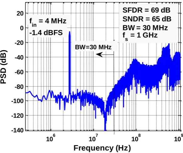
In the proposed design example the modulator loop filter is of order 2, the TDC resolution is 80 psec, the PWM center frequency, fc, is set to be 500 MHz while the TDC clock rate is 1 GHz. The simulated spectrum result shown in Fig. 10, confirms that there is a second order noise shaping in the modulator output signal and the achieved SNDR is 65 dB in a 30 MHz bandwidth. The point is that, this SNDR is obtained without using any complex and high power analog comparators, since the TDC is a fully digital and low power circuit.
5- CONCLUSION
In this paper, a brief review is devoted to the newly-developed generation of the ADCs, named as time-based ADCs. The advantages of the time-based quantization approach are introduced. Two kinds of well-known time-based sigma-delta modulators, VCO-time-based and TDC-based ADCs, are reviewed and their advantage and disadvantages are highlighted. As a design example, a closed-loop continuous-time TDC-based sigma-delta modulator is proposed and its simulation results are given to confirm the effectiveness of the time-based approach.
REFERENCES
[1] T. Christopher, Analog-to-Digital conversion via time-mode signal processing, Ph.D. Dissertation, Dept of Electrical and Computer Engineering, McGill University, Montreal, 2007.
[2] Y. Fei, “Design techniques for time-mode noise-shaping analog-to-digital converters: a state-of-the-art review,” Analog Integrated Circuits and Signal Processing, vol. 79. pp 191–206, Nov. 2014.
[3] S. Norsworthy, R. Schreier, and G. Temes, Delta-Sigma Data Converters: Theory, Design and Simulation. New York: IEEE Press, 1997.
[4] J. M. de la Rosa et al., “Sigma-Delta Modulators: Tutorial Overview, Design Guide, and State-of-the-Art Survey,” ,” IEEE Trans. Circuits Syst. I, Reg. Papers, vol. 58, no. 1, pp. 1–21, Jan. 2011.
[5] M. Z. Straayer and M. H. Perrott, “A 12-bit, 10-MHz bandwidth, continuous- time ΔΣ ADC with a 5-bit, 950-MS/s VCO-based quantizer,” IEEE J. Solid-State Circuits, vol. 43, no. 4, pp. 805– 814, Apr. 2008.
[6] B. D. Vuyst, and P. Rombouts, “A 5-MHz 11-bit self oscillating ΣΔ modulator with a delay-based phase shifter in 0.025 mm2,” IEEE J. of Solid-State Circuits, vol. 46, no. 8, pp. 1919–1927, Aug. 2011.
[7] A. Iwata, “The architecture of delta sigma analog-to-digital converters using a VCO as a multi-bit quantizer,” IEEE Trans. Circuits and Systems-II: Exp. Briefs, vol. 46, no. 8, pp. 941 –945, Aug. 1999.
[8] B. Drost et al., “Analog Filter Design Using Ring Oscillator Integrators,” IEEE J. Solid-State Circuits, vol. 47, no. 12, pp. 3120–3129 Oct. 2012.
[9] J. Kim, T. K. Jang, Y. G. Yoon, and S. Cho, “Analysis and design of voltage-controlled oscillator based analog-to-digital converter,” IEEE Trans. Circuits Syst. I, Reg. Papers, vol. 57, no. 1, pp. 18– 30, Jan. 2010.
[10]M. Park, and M. H. Perrott, “A 78 dB SNDR 87 mW 20 MHz bandwidth continuous-time ΣΔ ADC with VCO-based integrator and quantizer implemented in 0.13 m CMOS,” IEEE J. Solid-State Circuits, vol. 44, no. 12, pp. 3344–3358, Dec. 2009.
[11]K. Reddy, S. Rao, R. Inti, B. Young, A. Elshazly, M. Talegaonkar, and P. Hanumolu, “A 16-mw 78-dB SNDR 10-MHz BW CT DR ADC using residue-canceling VCO-based quantizer.” IEEE J. Solid-State Circuits, vol. 47, no. 12, pp 1–12, Dec. 2012.
[12]G. Taylor and I. Galton, “A mostly digital variable-rate continuous-time ADC ΔΣ modulator,” in Proc. IEEE ISSCC, pp. 298–299, Feb. 2010.
[13]S. Rao, B. Young, A. Elshazly, W. Yin, N. Sasidhar, and P. Hanumolu, “ A 71 dB SFDR open loop VCO-based ADC using 2-level PWM modulation,” in Proc. IEEE Symp. VLSI Circuits Digest of Technical Papers, pp. 270-271, Jun. 2011.
[14]S. Zaliasl et al., “A 12.5-bit 4MHz 13.8mW MASH ΣΔ modulator with multirated VCO-based ADC,” IEEE Trans. Circuits Syst. I, Reg. Papers, vol. 59, no. 8, pp. 1604–1613, Aug. 2012.
[15]G.W. Roberts, and M. Ali-Bakhshian, “A Brief Introduction to Time-to-Digital and Digital-to-Time Converters,” IEEE Trans. Circuits and Systems-II: Exp. Briefs, vol.57, no.3, pp.153-157, March 2010.
[16]D. I. Porat, “Review of sub-nanosecond time-interval measurements,” Nuclear Science, IEEE Transactions, vol 20, no .5, pp.36-51 , October. 1973.
[18]L. Hernandez, and E. Prefasi, “Analog to digital conversion using noise shaping and time encoding,” IEEE Trans. Circuits Syst. I, Reg. Papers, vol. 55, no. 8, pp. 2026–2037, Aug. 2008.
[19]E. Prefasi, L. Hernandez, S. Paton, A. Wiesbauer, R. Gaggl, and E. Pun, “A 0.1 mm , wide bandwidth continuous-time sigma delta ADC based on a time encoding quantizer in 0.13 um CMOS,” IEEE J. Solid-State Circuits, vol. 44, no. 10, pp. 2745–2754, Oct. 2009.
[20]C. Taillefer, and G. Roberts, “Delta-sigma A/D converter via time-mode signal processing,” IEEE Trans. Circuits Syst. I, Reg. Papers, vol. 56, no. 9, pp. 1908–1920, Sept. 2009.
[21]M. Straayer, M.H. Perrott, “A 10-bit 20 MHz 38 mW 950 MHz CTRDADC with a 5-bit noise-shaping VCO-based quantizer and DEM circuit in 0.13µm CMOS.” in Proc. IEEE Symp. VLSI Circuits Digest of Technical Papers, pp. 246–247, Jun. 2007.
[22]M. Park, and M. H. Perrott, “A single-slope 80 Ms/s ADC using two-step time-to-digital conversion.” in Proc. IEEE Symp. Circuits and Systems, pp. 1125– 1128, May. 2009.
[23]S. Zaliasl et al., “A 77 dB SNDR, 4MHz MASH ΔΣ modulator with a second-stage multi-rate VCO-based quantizer.” in Proc. IEEE Symp. Custom Integrated Circuits Conference (CICC), pp. 1–4, Sept. 2011.
[24]V. Dhanasekaran et al., “A 20 MHz BW 68 dB DR CT ΔΣ ADC based on a multibit time-domain quantizer and feedback element.” in Proc. IEEE Symp. International Solid-State Circuits Conference Digest of Technical Papers (ISSCC), pp. 174–175, Feb. 2009.
[25]P. Gao, X. Xing, J. Cranincks, and G. Gielen, “ Design of an intrinsically linear double-VCO-based ADC with 2nd-order noise shaping.” in Proc. IEEE Symp. Design, Automation & Test in Europe Conference and Exhibition, pp. 1215–1220, Mar. 2012.
[26]T. Jang, J. Kim, Y. Yoon, and S. Cho, “A highly-digital VCO-based analog-to-highly-digital converter using phase interpolator and digital calibration.” IEEE Trans. VLSI Systems, vol. 20, no. 8, pp. 1368–1372, Aug. 2012.
[27]Y. Yoon, S. Park, and S. Cho, “A time-based noise shaping analog-to-digital converter using a gated-ring oscillator.” in Proc. IEEE Symp. MTT-S International Microwave Workshop Intelligent Radio for Future Personal Terminals, pp. 1–4, Aug. 2011.
[28]U. Wismar, D. Wisland, and P. Andreani, “A 0.2V 0.44µW 20KHz Analog to Digital ΣΔ modulator with 57 fJ/conversion FoM.” in Proc. IEEE Symp. European Solid-State Circuits Conference (ESSCIRC) pp. 187–190, Sept. 2006.
[29]Y. Tousi, and E. Afshari, “A miniature 2 mW 4 bit 1.2 GS/s delay-line-based ADC in 65 nm CMOS.” IEEE J. Solid-State Circuits, vol. 46, no. 10, pp. 2312–2325, Oct. 2011.
[30]A. Gelb and W. V. Velde, Multiple-Input Describing Functions and Non-Linear System Design, New York: McGraw-Hill, 1968.
[31]E. Roza, “Analog-to-digital conversion via duty-cycle modulation,” IEEE Trans. Circuits and Systems-II: Exp. Briefs, vol. 44, no. 11, pp. 907–914, Nov. 1997.
[32]M. Tamaddon, and M. Yavari, “An NTF-Enhanced Time-Based Continuous-Time Sigma-Delta Modulator,” Journal of Analog Integrated Circuits and Signal Processing, vol. 85, no. 2, pp. 283-297, Nov. 2015.
![Fig. 3. Frequency-mode VCO-based ADC, (a) the block diagram,(b) its linearized model [7]](https://thumb-us.123doks.com/thumbv2/123dok_us/17349.2001761/3.595.325.521.259.515/fig-frequency-mode-based-block-diagram-linearized-model.webp)